


I. Introduction
For the past few years, with the rapid development of advanced mobile communication technology, mobile devices have been increasingly miniaturized. Thus, antennas covering the wideband have been widely developed. However, owing to the space constraints of mobile devices, mobile antennas must likewise assume a smaller physical area. As the antenna’s area decreases according to its input impedance variation, the performance and bandwidth of small antennas will be relatively reduced. Simultaneously, the demand for an antenna designed with high efficiency and wide impedance bandwidth with limited clearance has been increasing. Hence, increasing antenna bandwidth technology in mobile communication is urgently needed in antenna design [1–3].
In previous studies, the methods of increasing impedance bandwidth can be roughly divided into two cases: changing the feeding structure to increase the loop resonance, thereby improving the antenna’s bandwidth, and the practical use of the planar inverted-F antenna (PIFA) owing to its compact structure, which is similar to that used for a monopole in mobile terminals [4]. The planar inverted-E (PIE) antenna is based on the PIFA feeding structure and is realized by adjusting the position of the shunt chip capacitor in the PIE antenna’s feeding structure to increase the resonance, thereby realizing a wide impedance bandwidth [5].
A loop-type antenna is designed to use spiral inductance and gap capacitance with a feeding structure to achieve wide bandwidth operation [6]. The other case is to add a conductor near the antenna’s printed circuit board (PCB) to generate parasitic resonance to increase the antenna’s impedance bandwidth. A patch dipole antenna printed board feeding in the center of the PCB and a chip balun are embedded therein to excite each radiator to achieve wideband impedance matching technology [7]. Using endless metal rims around the ground plane can improve the antenna’s performance [8]. Alternatively, placing a large evaluation board under the antenna and using a magnetic field to excite the board’s resonance would also achieve the expected increase in impedance bandwidth [9]. Furthermore, the planar slot antenna’s feeding structure is designed with a modified coplanar waveguide (CPW) feeding line for tuning and optimization to achieve a wide impedance bandwidth [10]. In practice, however, these approaches consume considerable physical space, and excessive costs may be incurred while significant antenna clearance space is used in the PCB. Thus, it is difficult to achieve the desired miniaturized mobile antenna.
This paper proposes a feeding structure with a series chip capacitor to control the coupling performance and a series chip capacitor to control the resonance frequency to achieve a wide bandwidth. The proposed antenna was designed in a ground plane. In a simulation, it attained a 400-MHz bandwidth, ranging from 680 MHz to 1,080 MHz, under a voltage standing wave ratio (VSWR) of 3:1. The experimental results also showed the satisfactory performance of the antenna. The average efficiency increased from 43.6% to 59.2% in the range of 690 MHz to 960 MHz. The proposed technology’s target frequency is intended to operate on the LTE B17 (704–746 MHz), B5 (824–894 MHz), and GSM900 (880–960 MHz) platforms. The proposed technology can be applied to different scenarios, including various sizes and modules of the evaluation board, disparate feeding structures, and size changes.
II. Antenna Design and Operation Principle
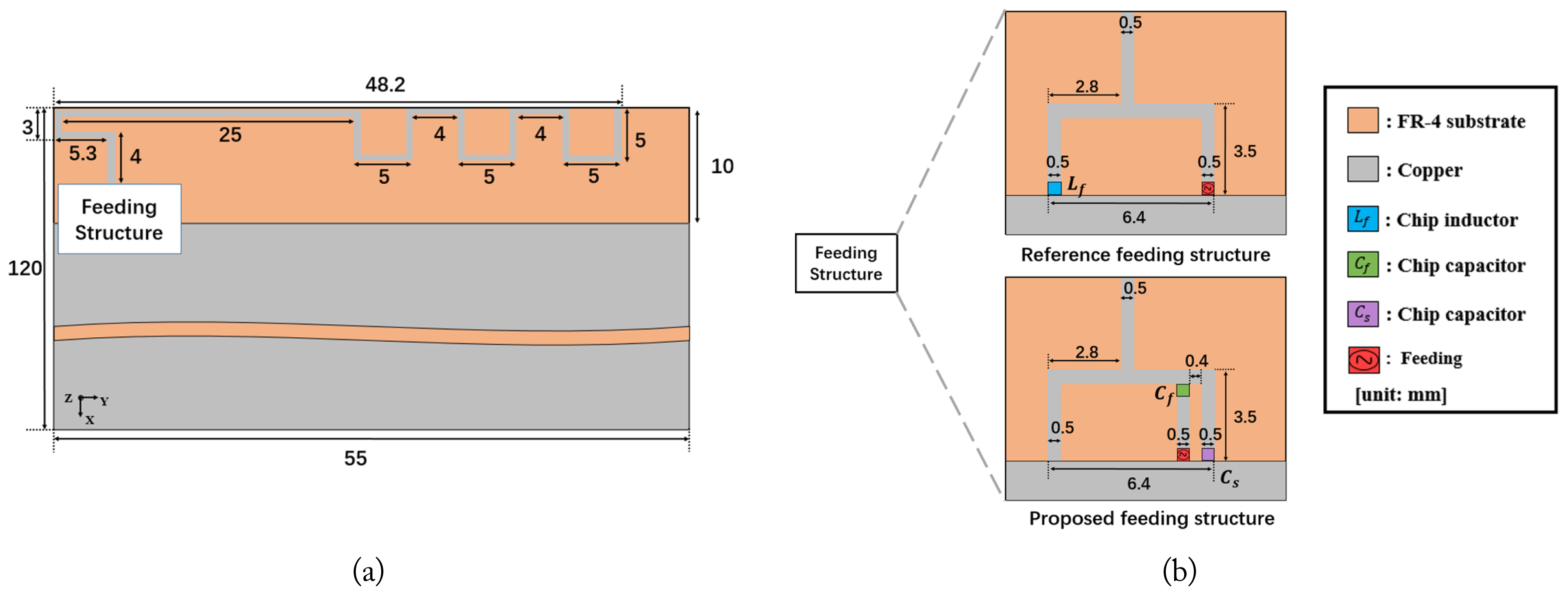
Fig. 1 shows a 120 mm × 55 mm × 1 mm board set on an FR-4 (Frame Retardant Type 4) substrate (ɛr = 4.4, tanδ = 0.02). The size of the ground plane is 110 mm × 55 mm with a clearance of 10 mm × 55 mm for the antenna. The width of the radiator in this experimental operation was 0.5 mm. The reference antenna and proposed antenna are simply quarter-wavelength (λ/4)-type antennas in the simulation. They all have a 3.5 mm × 6.4 mm feeding structure and a series chip inductor Lf (5 nH) connected to the ground plane with a shorting pin to achieve reference antenna impedance matching. A series chip capacitor Cf (3.2 pF) was connected to the feeding point, and a shunt chip capacitor Cs (2.5 pF) was used for the proposed antenna’s feeding structure. A radiator loop is connected to the top 2.8 mm position of the feeding structure to achieve the −6 dB bandwidth of the proposed antenna for 680 MHz to 1,080 MHz antenna applications. The −6 dB bandwidth equivalent to the VSWR of 3 is usually used, even though the VSWR of 2 is also used in some cases [11–13]. Fig. 2(a) shows the operating principle of the proposed antenna-feeding structure. The proposed antenna current mode diverges from that of the reference antenna with respect to the addition of a shunt line with a parallel chip capacitor (Cs), as the PIFA antenna forms only one loop current [14].
Two loop currents can be formed if the parallel chip capacitor (Cs) is added. The Loop 1 current consists of a shorting pin (Lf), series chip capacitor (Cf), and source. The Loop 2 current comprises a parallel chip capacitor (Cs) and shorting pin (Lf). The resonance frequency of Loop 2 can be controlled by the area of Loop 2 and the chip capacitor (Cs). The Loop 1 current is excited by the source, the Loop 2 current is excited by the Loop 1 current, and the coupling is represented by the following input impedance of the two-port network of the feeding structure as in the following equation [15]:
In Eqs. (1)–(5), Zin is normalized with respect to Z11, where the components LLoop1 and LLoop2 are the respective inductances of Loop 1 and Loop 2 in proportion to the square root of the loop area, including Lf. According to the reaction concept and the characteristic modes theory with conducting bodies, the coupling between Loop 1 and Loop 2 is shown in the second part of Eq. (1). When the series chip capacitance (Cf) method is not used, the proposed antenna coupling is poor because the feeding loop structure (Loop 1) is so small that the radiation performance is reduced [4].
Fig. 2(b) shows the operating principle of the feeding structure and radiator element of the proposed antenna, where components Lr, Cr, and Rr, respectively, represent the inductance, capacitance, and resistance of the radiator element. The Loop 2 current consists of the shorting pin (Lf) and the parallel chip capacitor (Cs), and it is excited by the Loop 1 current. The parallel chip capacitor (Cs) is determined by the resonant frequency of Loop 2. The radiator current comprises the proposed antenna radiator loop and is excited by Loop 2. Loop 2 and the radiator are represented by the following two-port impedance matrix [12]:
where ZLoop2 and ZRadiator are the impedances of feeding Loop 2 and the radiator. Zfs is the impedance of the shorting pin (Lf). As shown in Eq. (5), the coupling degree of the feeding structure and radiator element is determined by the shorting pin (Lf). The simulated surface current distributions of the reference antenna at 0.9 GHz are shown in Fig. 2(c), and the proposed antenna’s surface current distributions, as shown in Fig. 2(d), clearly show that there is more than one loop in the proposed feeding structure. During the feeding structure operation of the proposed antenna, the resonance frequencies of multiple Loop 1, Loop 2, and the radiator are set as the antenna’s operating frequency to achieve a wide impedance bandwidth.
III. Simulation Result and Control Method
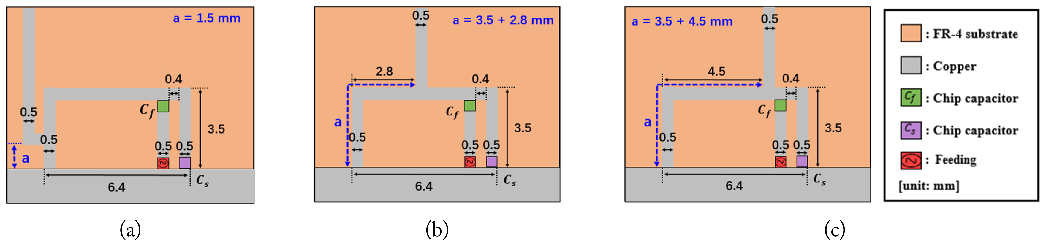
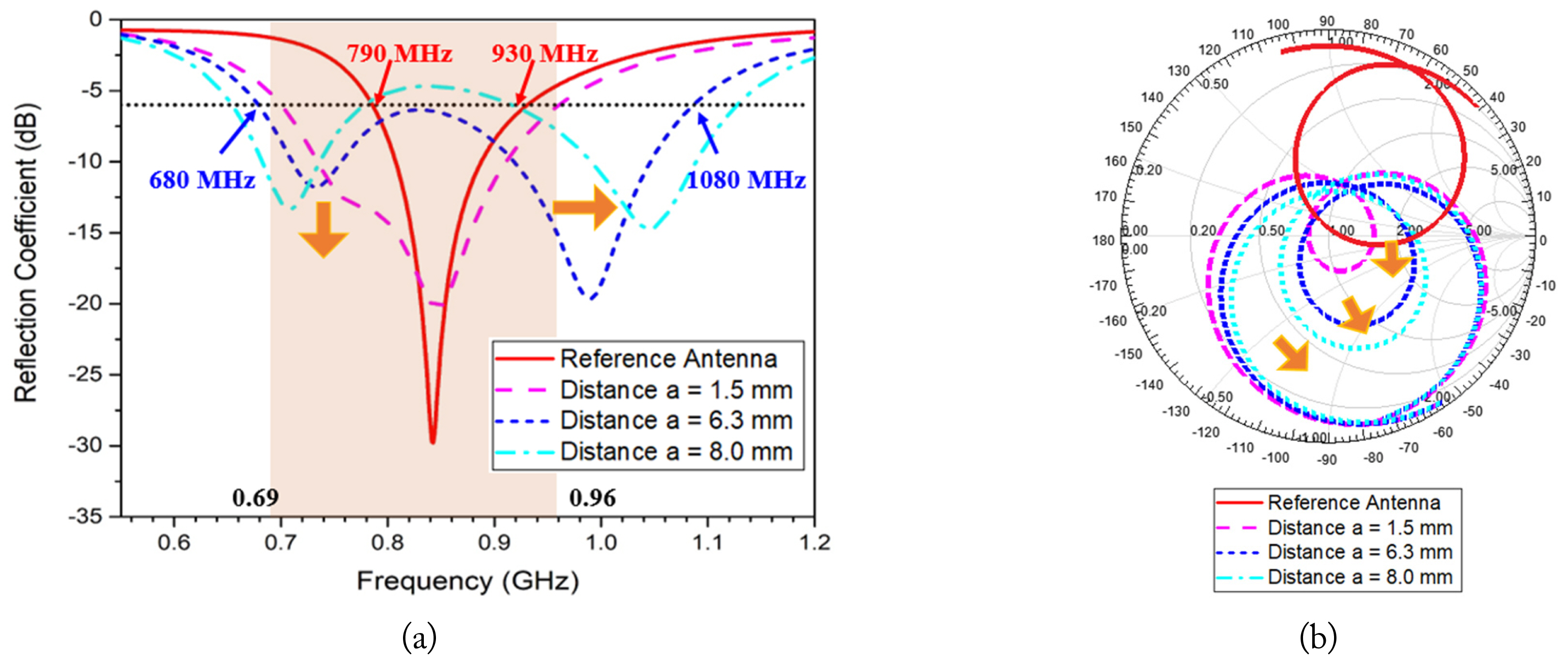
Fig. 3 shows that the radiator contact point moves on the proposed antenna’s feeding structure, with the distance “a” mm of the shorting pin with the ground plane junction point of the proposed antenna increasing by 1.5 mm to 8 mm (Fig. 4). Fig. 4(a) shows that the reference antenna without a parallel chip capacitor (Cs) can only produce a bandwidth of 140 MHz under a VSWR of 3:1 from 790 MHz to 930 MHz. The proposed antenna in the case of a = 6.3 mm (Cf = 3.2 pF, Cs = 2.5 pF) achieves a −6 dB bandwidth of 400 MHz (from 680 MHz to 1,080 MHz), as shown in Fig. 4(b). In addition to the reference antenna, each value corresponds to two resonance loci (impedance loci) in the Smith chart. The simulation results clearly show the long distance between the radiator and the loop structure, and the larger loci size of the small circle can be found in the Smith chart.
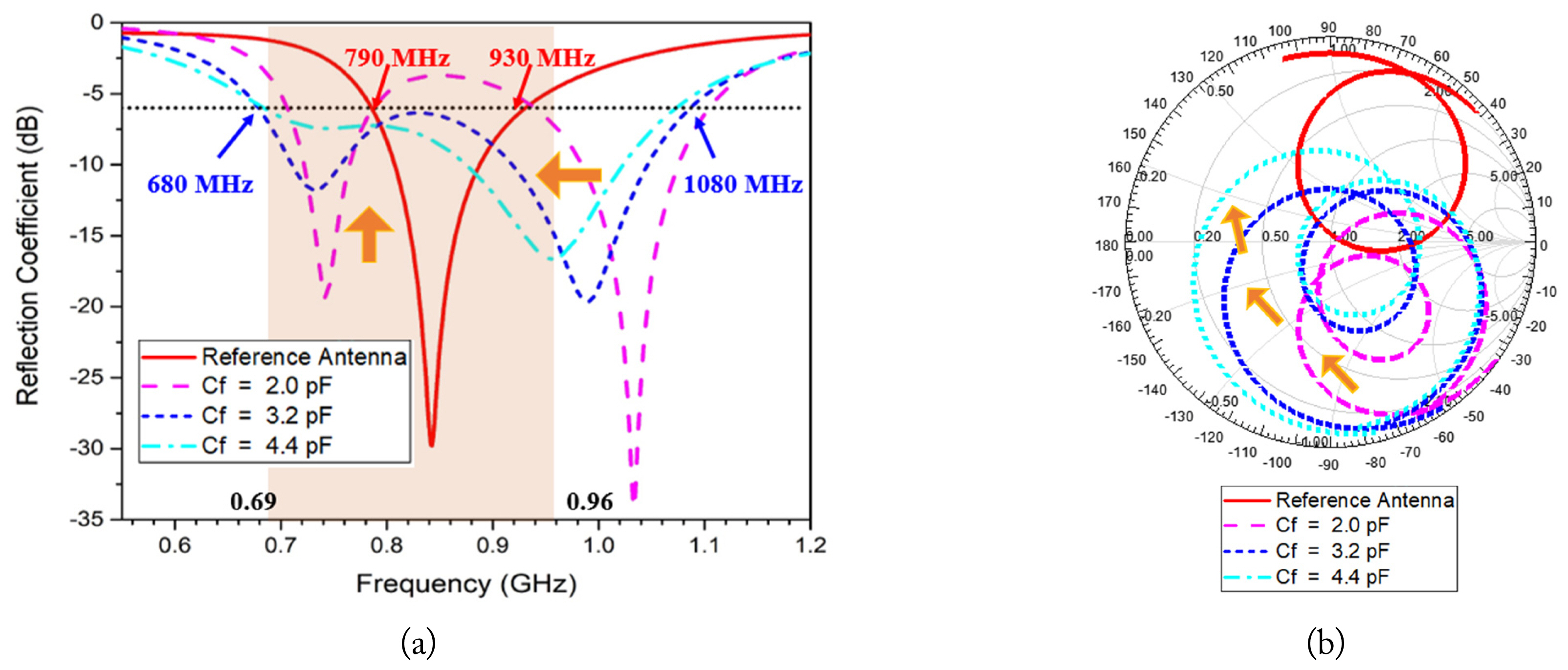
Fig. 5(a) depicts the reflection coefficients of the respective reference and proposed antennas with distinct series chip capacitor (Cf) values, ranging from 2.0 pF to 4.4 pF. It is clearly observed that, with the increase in the chip capacitor (Cf) value, the path of the large impedance locus extends outward (the coupling increasing gradually), as shown in Fig. 5(b).
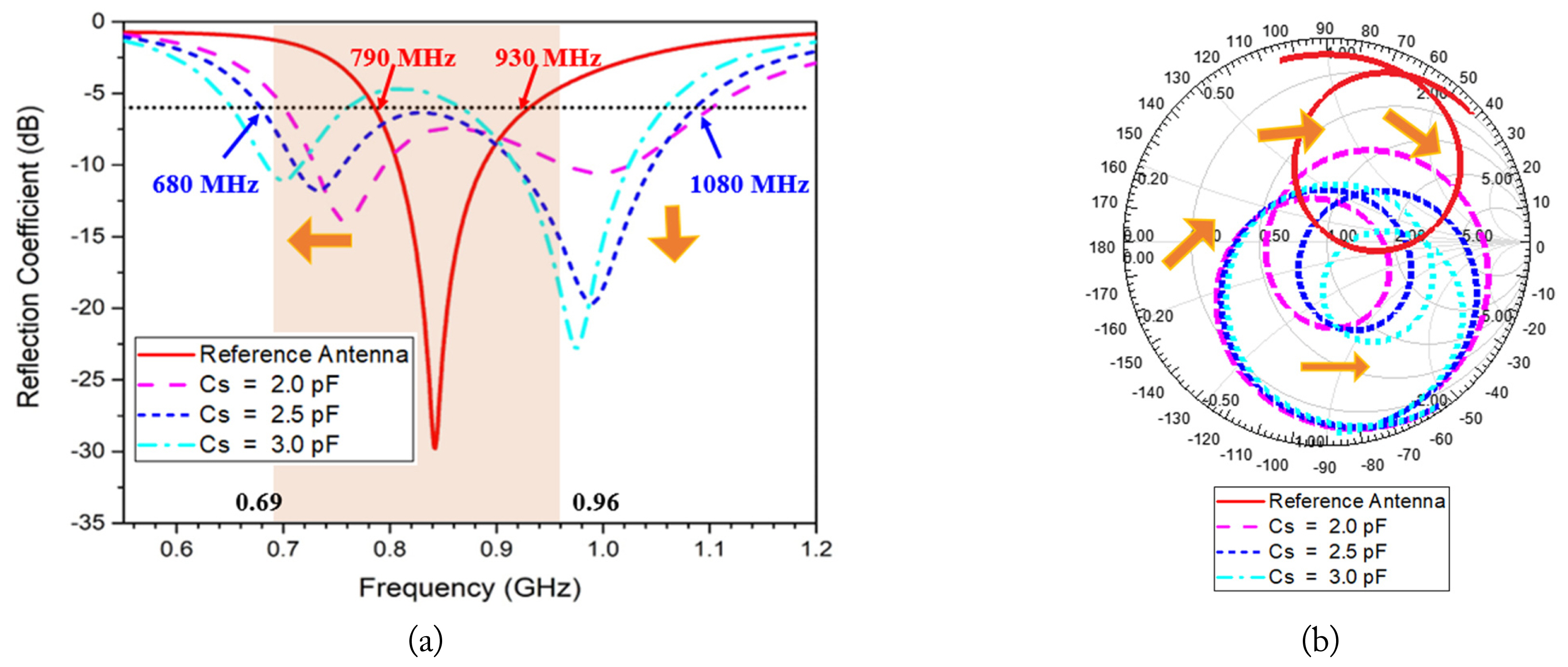
Fig. 6(a) shows the simulated reflection coefficients of the reference antenna and proposed antenna with disparate shunt chip capacitor (Cs) values, ranging from 2.0 pF to 3.0 pF. Fig. 6(b) depicts the impedance variation with the change in the value of the shunt chip capacitor (Cs). It is clearly observable that with the increase of the shunt chip capacitor’s (Cs) values, the path of the small locus circle rotates clockwise, and the resonance frequency slightly decreases with the reduction of the parallel chip capacitor’s (Cs) values. Correspondingly, the size of the large circle path in the Smith chart with the input impedance loci is determined by the series capacitor (Cf) values, and the frequency of the large circle path is determined by the parallel capacitor (Cs) value. Furthermore, the size of the small circle path in the Smith chart is determined by the contact point with the shorting pin (Lf) distance. The simulation experiment finally realized a −6 dB bandwidth of 400 MHz (range, 660–1,080 MHz) by using distance a = 6.3 mm, Cf = 3.2 pF, and Cs = 2.5 pF, under a VSWR of 3:1.
IV. Experimental Result
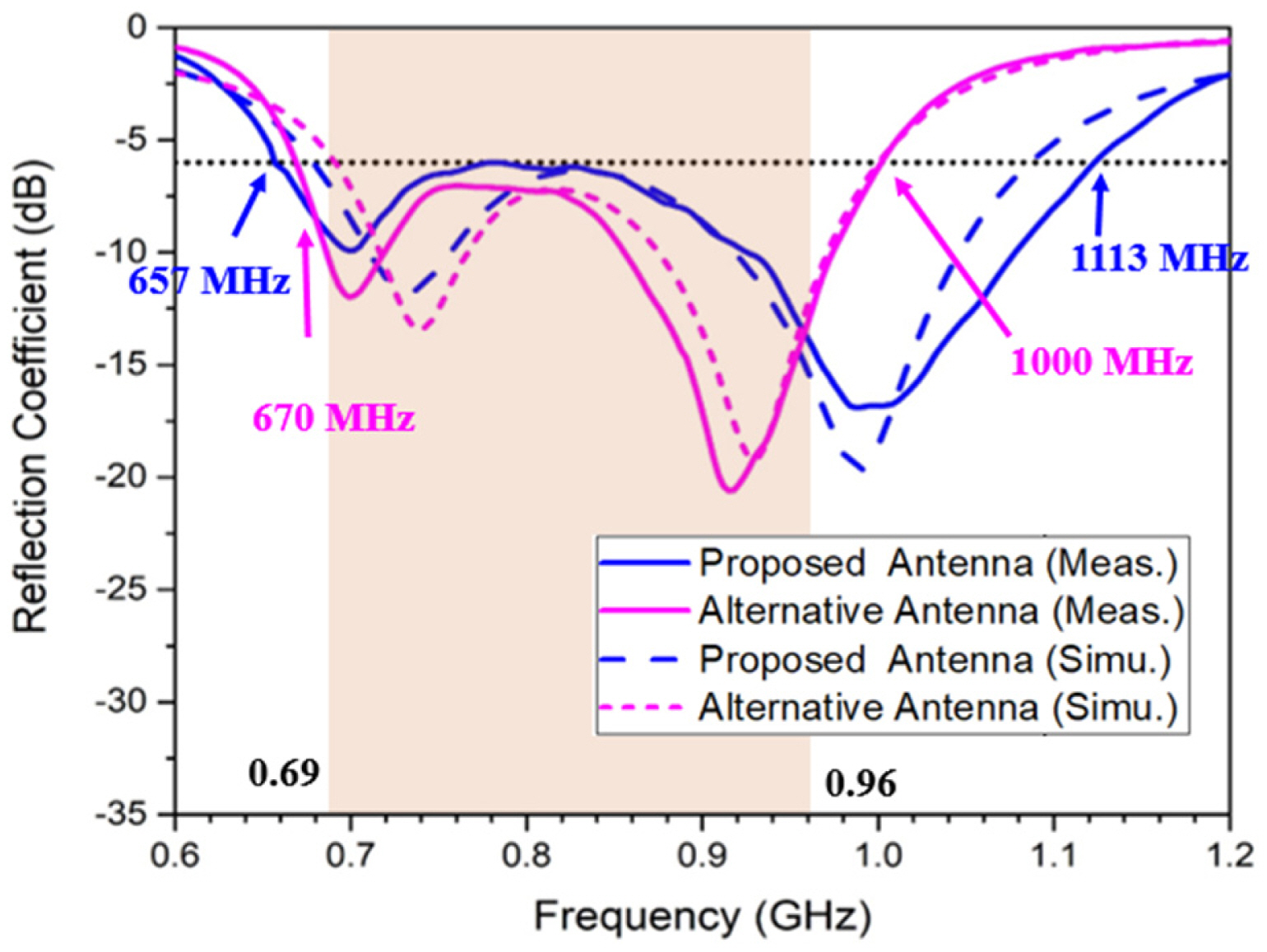
The reference and proposed antennas were fabricated and measured using the Agilent 8753ES network analyzers and a 3D CITA OTA chamber (sized 6 m × 3 m × 3 m). To complete input impedance matching for the reference antenna, the feeding structure series chip inductor value was set at 2.2 nH at the shutting pin contact point with the ground plane, and the series chip capacitor was 7 pF in the feeding structure. For the proposed antenna with the shunt chip capacitor, the Cs value in the feeding structure was 2.0 pF (4 pF series 4 pF), the series chip capacitor Cf value was 2.2 pF, and the radiator contact point with the ground plane distance was a = 3 mm. The measured reflection coefficients are conveyed in Fig. 7, where the −6 dB bandwidth is 162 MHz (790–952 MHz) for the reference antenna and 456 MHz (657–1,113 MHz) for the proposed antenna.
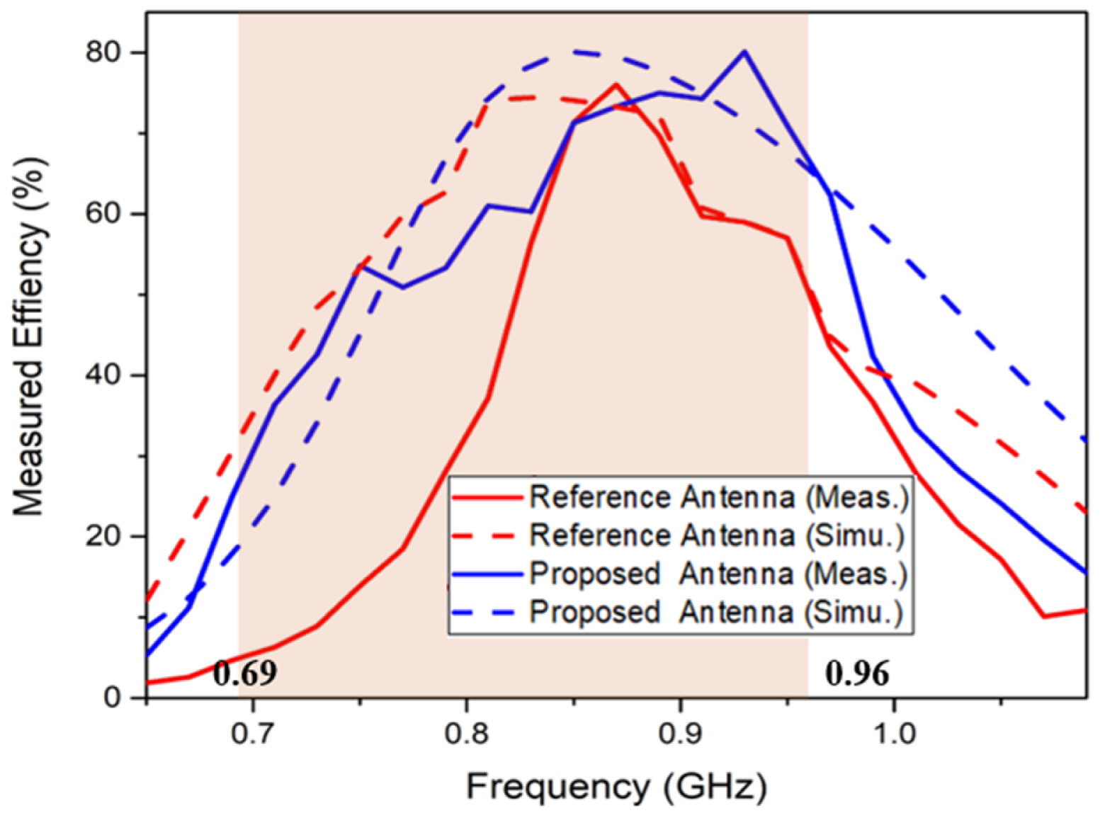
The measurement results showed similar characteristics to the simulation results. Fig. 8 demonstrates that the average measured efficiency of the reference antenna is 43.6% and that of the proposed antenna is 59.2% in the target frequency range (690–960 MHz). The efficiency data fully depict the satisfactory performance of the proposed antenna with a wide impedance bandwidth.
Fig. 9 illustrates the measured and simulated far-field theta (θ) and phi (ϕ) direction radiation patterns at 950 MHz. The far-field omnidirectional radiation patterns for the proposed antenna displayed good antenna performance. The measurement results convey that under the proposed technology, the proposed antenna has wider bandwidth and greater radiation efficiency than the reference antenna.
V. Alternative Design
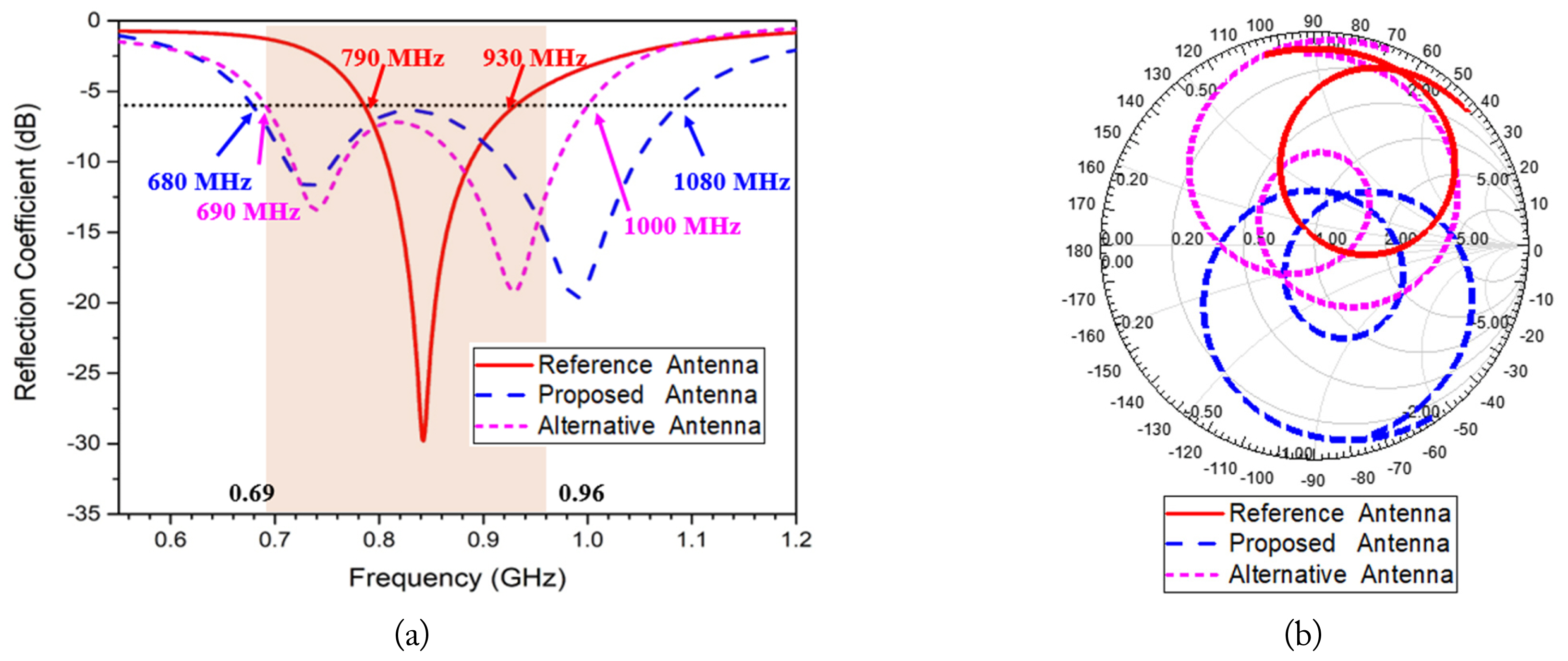
Another design comprising the alternative design and the proposed antenna is realized in Fig. 10. In the alternative design antenna feeding structure, the chip inductor (La) is a series in the feeding line instead of the chip capacitor (Cf), similar to the proposed antenna. The alternative design antenna feeding structure constitutes a parallel capacitor (Cs′) and shorting pin (Lf′). The parallel capacitor (Cs′) value is also determined by the appropriate resonance frequency, while the alternative design antenna feeding structure uses chip inductors to control the series resonance to achieve impedance matching. To compare the simulation results of the alternative design structure with those of the proposed antenna, the same radiator, position model, and feeding structure size as those of the proposed antenna were used in the experiment. A radiator with a length of 6.5 mm × 0.5 mm was added to the tail of the alternative antenna to conform to the desired frequency range (690–960 MHz).
For a more intuitive comparison of the experimental results, the simulated reflection coefficients of the reference antenna, proposed antenna, and alternative design antenna are presented in Fig. 11(a). It is evident that the alternative antenna (La = 9.5 nH, Cs′ = 4.8 pF) achieves a bandwidth of 310 MHz (690–1,000 MHz) under the VSWR of 3:1, as shown in Fig. 11(a). Its reflection coefficient is found to have characteristics similar to those of the proposed antenna with the alternative design antenna. The input impedance circle locus of the alternative design antenna is depicted in Fig. 11(b). The large circle size is determined by the shorting pin (Lf′) series with the same chip inductor (La) circuit resonance as the proposed antenna. The small circle position locus with an alternative design antenna is controlled with the parallel capacitor (Cs′) and shorting pin (Lf′). The small circle size is also determined by the shorting pin (Lf′). The alternative design antenna shows that the resonance of the feed loop structure can also be excited by the chip inductor, which plays a role in controlling the large circle with the coupling performance. This is consistent with the proposed antenna technique principle. The alternative design antenna’s simulation results also achieve a target frequency coverage of 690–960 MHz under the VSWR of 3:1. The alternative antenna measured reflection coefficient results also show similar characteristics to the simulation results, as shown in Fig. 12, where the −6 dB bandwidth of 330 MHz (670–1,000 MHz).
VI. Comparison and Discussion
Table 1 reveals the comparison results of the proposed antenna with previous studies in terms of antenna size, bandwidth, efficiency, operating frequency band, and type [5, 8, 9, 11, 16]. The proposed antenna has the advantage of easier manipulation of impedance matching compared to previous studies. It is easily observed that the proposed antenna has a wider bandwidth than the same type of antenna, with comparatively and relatively better efficiency in the same operating frequency band.
Murata capacitors (GRM Class-K within ±5% tolerance) and Murata inductors (LQG Class-S within ±10% tolerance) were used for the measurement [13]. For further investigation, the perfect lumped LC without loss is modeled in the simulation, where the tolerance value of the capacitors is within ±6.7% and the inductors are within ±10.9% while not apparently influencing the antenna’s performance. Tolerance in the simulation’s results is approximately consistent with that in the measurement results. Minor discrepancies are observed because of the fabrication error and the tolerance of electronic components between the measurement and simulation results. Hence, the comparison of the simulation and measurement data shows that the tolerance of the lumped elements does not significantly affect the experiment.
VII. Conclusion
In this paper, we proposed a feeding structure with a series chip capacitor to control the coupling performance and a parallel chip capacitor to control resonance frequency to achieve wide bandwidth technology. Simulation and measurement results were conducted for the proposed antenna. The simulation results illustrated a −6 dB bandwidth of 400 MHz (680–1,080 MHz), and the measurement results showed the realization of a −6 dB bandwidth of 456 MHz and improved efficiency compared to the reference antenna (43.6%–59.2%, 690–960 MHz). In the future, this technology can be applied to the design of miniaturized antennas to achieve a wider impedance bandwidth.