Design of a Wideband Balun Using IPD Technology for Compensating the Frequency Dependency
Article information
Abstract
In this paper, we propose a wideband balun using integrated passive device (IPD) technology. The proposed circuit is designed to compensate for the magnitude deviations by differentiating the magnitude S-parameter and calculating the lumped component value when the derivative value is zero. For a smaller size, the proposed circuit is implemented using IPD technology, and the fabricated circuit’s size is 2.4 mm × 1.02 mm. The magnitude of the measurement results has 3.5 ± 0.3 dB deviations from 2.8–4.58 GHz, and the phase difference has 180° ± 10° from 2.8–5 GHz at the center frequency of 3.6 GHz. Therefore, the measurement results show that the theory of the proposed circuit is well matched compared with the measurement results for smaller sizes, wideband magnitude, and phase characteristics.
I. Introduction
In wireless systems, a balun is vital in converting unbalanced signals to balanced ones or vice versa. Traditionally, baluns are made in low-temperature co-fired ceramic (LTCC) and monolithic microwave integrated circuits (MMIC) technologies. Commercially, baluns are implemented in LTCC technology, but recently, there has been a movement of technology to integrated passive device (IPD) technology for miniaturization and integrated circuits. Much research has been conducted to incorporate individual baluns [1, 2]. Most of them are baluns using transmission lines developed for RF applications. The circuits using transmission line topology are larger in size because of multiple λ/4 wavelengths.
Thus, many papers have suggested that the lumped LC passive component provide a size reduction [3–9]. However, these papers’ suggestion has the effect of reducing the target bandwidth due to frequency-dependent factors. The conventional work in [10] is implemented with low-pass filter (LPF) and high-pass filter (HPF) structures using lumped elements, but it is difficult to obtain a uniform magnitude characteristic. Thus, magnitude balance and phase difference are uniform only at the center frequency. However, as magnitude balance deviates from the center frequency, the magnitude and phase deviation increase.
In this paper, we propose a wideband balun using through-silicon via (TSV) IPD technology. The TSV process provides a solid ground plane with a copper layer at the wafer’s backside. The design minimizes GND influence from external packaging variation sources, and the overall tolerance is primarily controlled by the wafer manufacturing variation [11]. Reduced thermal resistance through the backside via [12] and excellent thermal conductivity of evenly distributed thick copper plane improves thermal performance, which is critical for compatible use with high-power gallium nitride (GaN). The proposed balun is composed of lumped components, and the component values are derived by differentiating the magnitude of the S-parameter with the constant value. The proposed balun implemented using IPD technology to smaller and low loss.
II. Design Theory and Simulation Results
1. Design Theory
An ideal balun consists of distributed lines using λ/4 and 3λ/4 of differential electrical lengths with
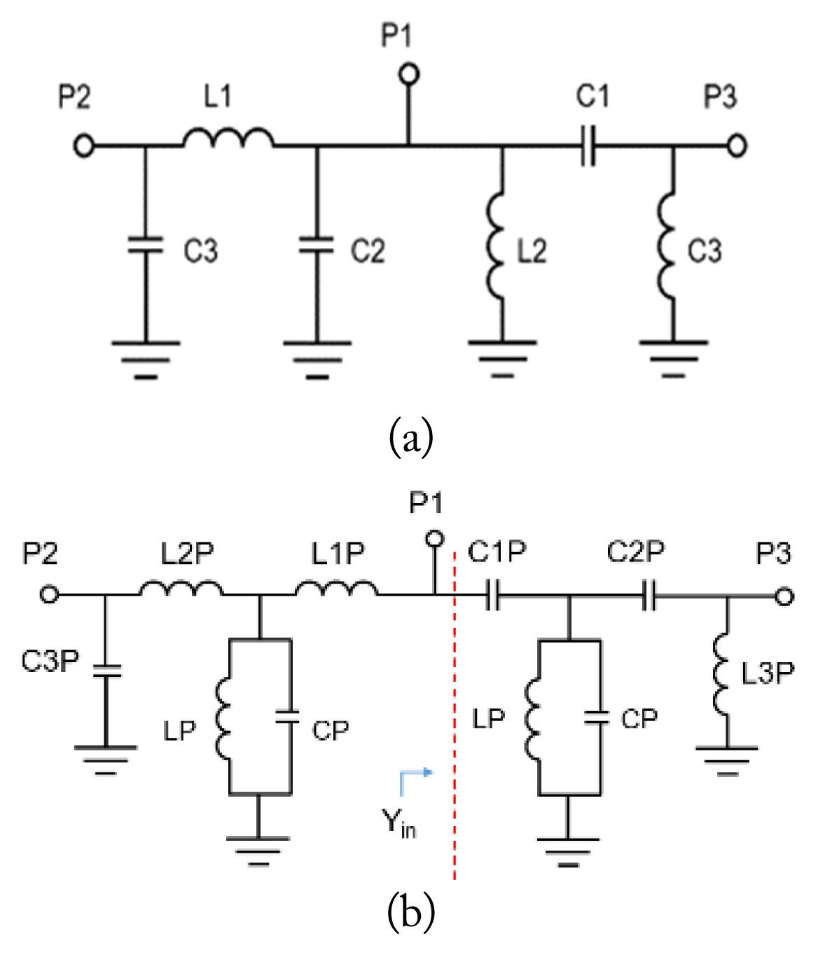
The inserted parallel resonator is an open circuit at the resonant frequency, and the inserted resonator serves to control the deviated magnitude values to constant values. To derive the element values of the proposed circuit of Fig. 1(b), Eq. (1) is obtained by terminating Port 3 as Z0, which is the ABCD parameter between Ports 1 and 2.
Similarly, the ABCD parameters obtained between Ports 1 and 3 are derived by A2, B2, C2, and D2, as shown in Eq. (2). The input admittance Yin terminated as Y0 at Port 3 in Fig. 1(b) is expressed as Eq. (3).
The total ABCD parameter is obtained between Ports 1 and 2 using the cascaded Yin and A1, B1, C1, and D1 parameters as Eq. (4).
Eq. (4) is arranged as AT = A1, BT = B1, CT = A1Yin + C1, and DT = B1Yin + D1. Using the relation between the S-parameter and the ABCD parameter, S21 is obtained as Eq. (5).
The magnitude of S21 is shown as Eq. (6).
By differentiating the magnitude of the derived |S21|, the derived |S21| must be frequency independent in terms of the frequency over a wide bandwidth. The differential value of the derived |S21| at the center frequency ω0 is zero to make the frequency-dependent term reduced in wideband; then the value of LP is expressed as Eq. (7).
The CP of the inserted parallel resonant values are derived from the resonant circuit.
2. Circuit Simulation Results
To verify the derived theory, the conventional circuit in Fig. 1(a) and the proposed circuit in Fig. 1(b) must be compared. The center frequency is 3.6 GHz, and the conducted simulation tool is Ansys, Electronics Desktop. The obtained values of Fig. 1(a) and 1(b) are shown in Table 1.
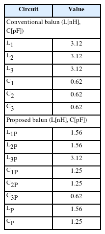
Element values of the conventional and proposed circuits
Fig. 2(a) and 2(b) show the circuit simulation results of the conventional and proposed circuits. The conventional circuit has variations ranging from −2.3 to −5.8 dB, while the proposed circuit has a constant value from −2.893 to −3.117 dB from 2.8 to 4.4 GHz. From the simulation results, the magnitude balance of the proposed circuit is compensated using design theory.
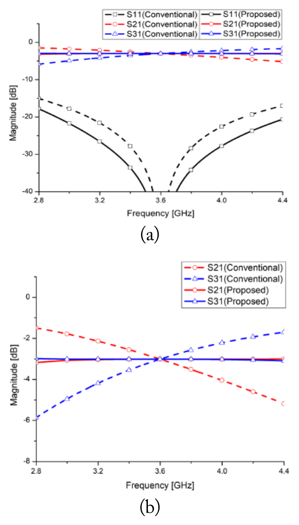
Comparison results of conventional and proposed baluns: (a) the magnitude and (b) the enlarged magnitude of S21 and S31.
III. 3D Structure and Fabrication Results
Fig. 3(a) and 3(b) show the layer configuration of the IPD inductor and capacitor, respectively. It is a cross-section view in which several layers of silicon nitride (SiN) and metal are stacked on silicon carbide (SiC). The inductor consists of M1 (Metal1) and M3 (Metal3) layers and is implemented in the form of a spiral inductor using M1 of the SiN2 layer. Then, the M1 and M3 layers are connected using the SNO2 (SiN open) metal layer penetrating the SiN3 dielectric (DE) layer. The capacitor uses M2 and M3 layers and is implemented in the form of a metal-insulator-metal (MIM) capacitor by inserting a SIN3 DE layer between the metals. A DE layer is inserted between each metal layer of the inductor and capacitor to prevent short circuits. Table 2 shows the details of the layers used in the structure of Fig. 3.

Layer structure of the IPD: (a) inductor and (b) capacitor.

Information of IPD layer
Fig. 4(a) and 4(b) show a spiral inductor and capacitor implemented as an IPD, respectively. Inductors require 1.56 nH and 3.12 nH for the design of the proposed balun at 3.6 GHz. Capacitors require 1.2 pF and 0.56 pF for the proposed balun. Fig. 4(c) is the proposed balun. The ground passing through the SiC layer is designed using the TSV method, which is implemented in the circuit in the form of back via (BVIA). In addition, the designed ground-signal-ground (GSG) pad is inserted at the input and output ports for measurement. The total size of Fig. 4(c) is 2.4 mm × 1.02 mm.
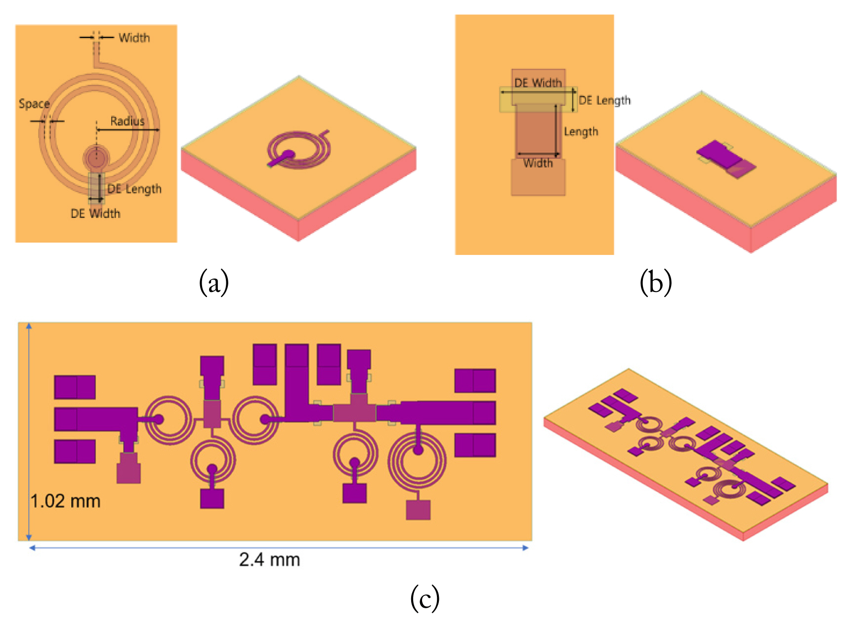
(a) The IPD structure of the inductor, (b) the IPD structure of the capacitor, and (c) the 3D structure of the proposed IPD balun.
Fig. 5 is the microphotograph of the proposed balun fabricated by an IPD. The implemented structure shows that the designed 3D structure is well implemented.
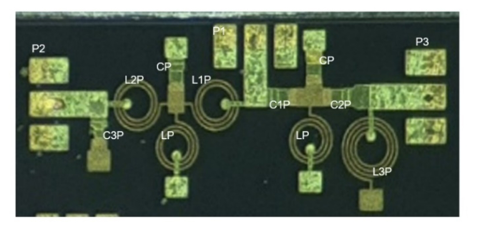
Microphotograph of the fabricated balun.
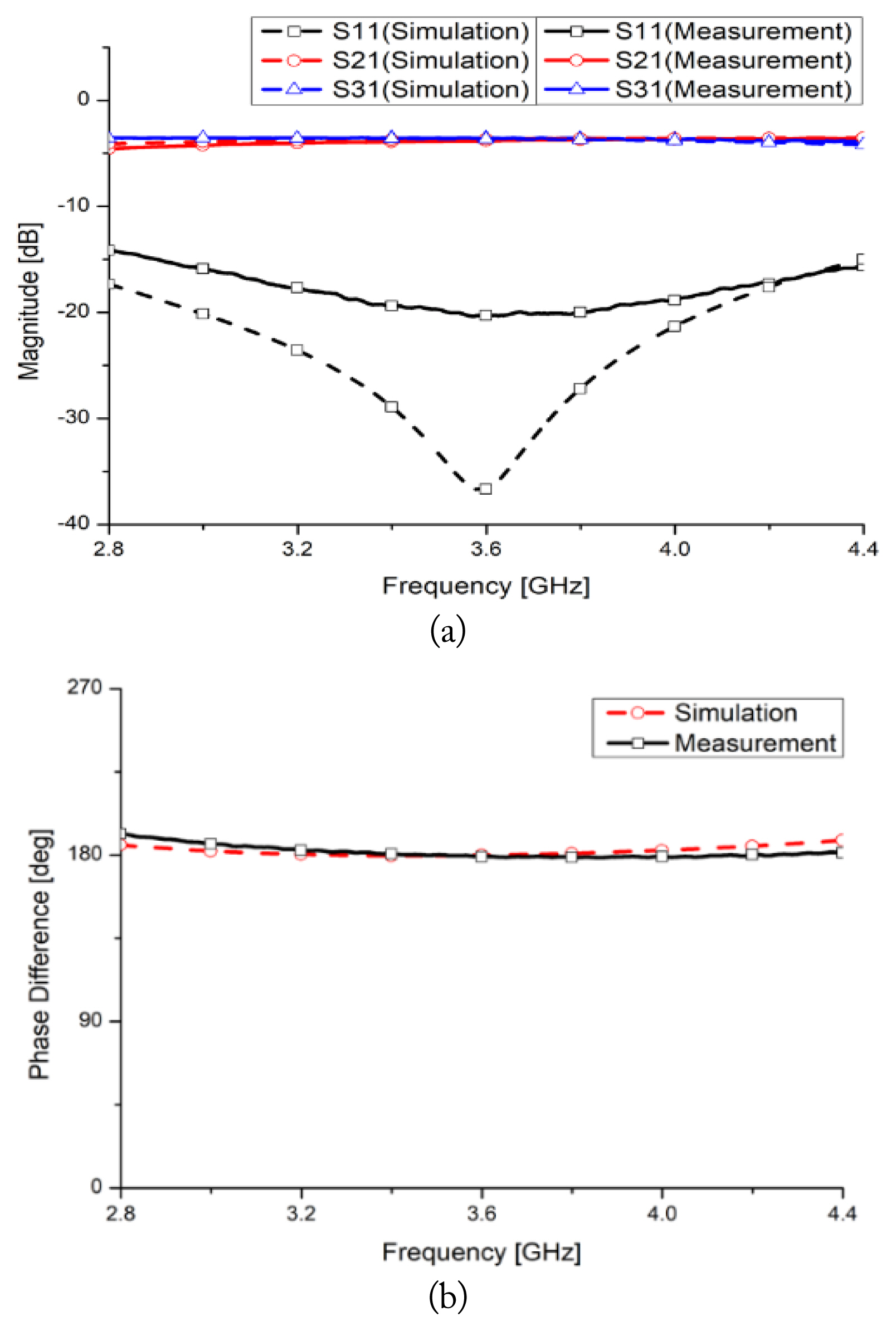
Fig. 6(a) and 6(b) show the magnitude and phase difference results measured with Agilent Network Analyzer (N5230) by uploading the proposed balun made with an IPD to Cascade Microtech probe station (Probe station summit 11741B). Fig. 6(a) is the comparison results according to the ±0.2 dB magnitude results within 2.96–4.2 GHz. Fig. 6(b) is the comparison results according to the phase difference from 2.96–4.2 GHz with ±3°. The measured results have a fabrication error since the capacitor is dominantly affected by the DE thickness between metals.
The comparison results of the performance according to the IPD technology are listed in Table 3, which shows that the balun has the center frequency, amplitude imbalance, phase imbalance, and fractional bandwidth (FBW) based on a 15-dB return loss. Therefore, using the proposed design method, the proposed circuit has excellent measurement results according to the amplitude, phase imbalance, and FBW.
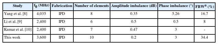
Performance comparison results of the previous works
IV. Conclusion
In this paper, we proposed a wideband balun using IPD technology for smaller sizes and low insertion loss. The proposed balun is designed to maintain the magnitude slope constant. By differentiating the magnitude, the component values of the proposed balun are derived. The magnitude balance and phase differences resulted in about 0.2 dB and 3° from 2.96 to 4.2 GHz. Thus, the frequency dependency of the proposed circuit is well compensated for not only magnitude balance but also phase difference.
Acknowledgments
This result was supported by “Regional Innovation Strategy (RIS)” through the National Research Foundation of Korea (NRF) funded by the Ministry of Education (MOE) (No. 2021RIS-004) and the Soonchunhyang University Research Fund.
References
Biography

Youna Jang received her master’s in display engineering from Hanyang University, Seoul, Korea, in 2014. She also received her Ph.D. in electrical communication system engineering from Soonchunhyang University, Choongnam, Korea, in 2019. She participated as a designer of the Duplexer filter in an internship program in 2015 at Qorvo, Bundang, South Korea. She was a lecturer at Soonchunhyang University from 2016 to 2020. She is currently a research professor at the Radio and Mechatronics Research Center. Her research areas include the design of passive components in microwave bands.

Kwanhun Jeong was born in Mokpo, Korea, in 1994. He received his B.E. degree in electrical engineering from Soonchunhyang University, Asan, Korea, in 2020. Currently, he received his master’s in ICT convergence at Soonchunhyang University. His current research interests include RF passive device theory, design, and testing. Currently, he joins the FAB Group at Wavice.

Yea-Ji Lee was born in Seoul, South Korea, in 1996. She received her bachelor’s in electrical engineering from Soonchunhyang University, Asan, South Korea. She received his master’s in ICT convergence at Soonchunhyang University. Her current research interests include RF filter design and testing and passive device. Currently, she joins the Interconnect Part team at Gigalane.

Taehoon Kang was born in Incheon, Korea, in 1993. He received his M.S. degree from Soonchunhyang University, Asan, Korea, in 2019. Currently, he is studying for a Ph.D. at Soonchunhyang University. His current research interests include RF filter theory, design, and testing.
Sangmin Lee received his Ph.D. in solid state Physics at Sogang University, Korea, in 1996. From 1996 to 1998, he was a postdoc at ETRI, developing InP-based photonic integrated circuits. From 2000 to 2005, he worked at UCSB and GCS, developing InP-based DHBT devices. In 2005, he started working on GaN HEMT devices for RF applications at various companies in the US, including RFMD and Cree. He was a qualification manager at RFMD and a research scientist at Cree. He joined the GaN HEMT R&D team at Gigalane in 2015, which became Wavice in 2017, as a CTO working on the R&D of RF GaN HEMT device technologies. He is currently a vice president of technonlogy at Global Communication Semiconductors, LLC in California, USA.
Seo Koo was born in Seoul, Korea, in 1990. He received his M.S. degree from Soonchunhyang University, Asan, Korea, in 2018. Currently, he is studying for a Ph.D. at Soonchunhyang University. His current research interests include RF filter theory, design, and testing.
Dal Ahn received his B.S., M.S., and Ph.D. degrees in electronics from Sogang University, Seoul, Korea, in 1984, 1986, and 1990, respectively. From 1990 to 1992, he worked with the Mobile Communications Division, Electronics, and Telecommunications Research Institute (ETRI), Daejeon, Korea. Since 1992, he has been affiliated with the department of Electrical Engineering, Soonchunhyang University, Asan, Chungnam, Korea, where he is currently a professor. Currently, he is also the chief of the RF and Microwave Component Research Center (RAMREC) at Soonchunhyang University. In addition, he is a technical consultant for Tel Wave Inc., Suwon, Korea. His current research interests include the design and application of passive and active components at radio and microwave frequencies, the design of RF front-end modules for various handset systems using low-temperature co-fired ceramic (LTCC) technology, DGS circuit applications, and circuit modeling using a commercial EM analysis program. Prof. Ahn is also an editor of the Journal of Korea Electromagnetic Engineering Society and a senior member of the Korea Electromagnetic Engineering Society (KEES).