A New Doherty Combiner with Wide Bandwidth for Magnitude and Phase Balance Compensation
Article information
Abstract
This paper proposes a novel Doherty combiner that uses a series and parallel resonant circuit for wideband. Unlike conventional combiners, the aim of the proposed combiners is to extend bandwidth for not only the magnitude bandwidth, but also phase balance by employing series and parallel resonant circuits at the output impedance of the peaking amplifier. Considering the load impedance of the peaking amplifier, the Doherty combiners were analyzed in the theory of this study by deriving the series and parallel resonant circuit values. The output phase balances are determined for the targeted bandwidth to achieve uniform phase balance in the proposed combiner I using a series resonator. For better magnitude bandwidth, the slope of reflection coefficient (Γ) at port 3 in the combiner II using series resonator was derived using the derivative of Γ with respect to ω. Experimental results show that the proposed combiner I has 63.5% magnitude fractional bandwidth (FBW) and 118% FBW with the phase balance at ±2.5°. The proposed combiner II also has 85% magnitude FBW and 118% FBW with the phase balance at ±2.5°.
I. Introduction
RF power amplifiers used in communication base stations require high efficiency and linearity. The amplifier needs to operate at high efficiency at a back-off level [1]. However, the base station power amplifiers have low efficiency due to the back-off operation [2]. Lower efficiency causes several thermal issues and decreases the lifetime of high-power transistors [3–5]. Therefore, much research [6–12] focusing on the large back off power region has been suggested in order to improve the average efficiency of power amplifiers, one of which is commonly known as the Doherty power amplifier, first proposed by Doherty [7] in 1936, as shown in Fig. 1(a). Various applications based on improving power efficiency in Doherty power amplifiers have been researched [8–12]. These include the multiway [8, 9], symmetric way [10], and asymmetric methods [11, 12]. However, Doherty power amplifiers and other applications [7–12] require λ/4 impedance transformers in splitting and combining operations for the two signals of the carrier and peaking amplifiers. These methods operate only near the center frequency, resulting in bandwidth limitations. Another requirement for power amplifiers is the ability to operate in wide bandwidth, as well as high linearity and high efficiency in the base station. Suggestions have been offered for better bandwidth [13–20], but these combiners have a phase balance limitation, despite the enhanced magnitude bandwidth.
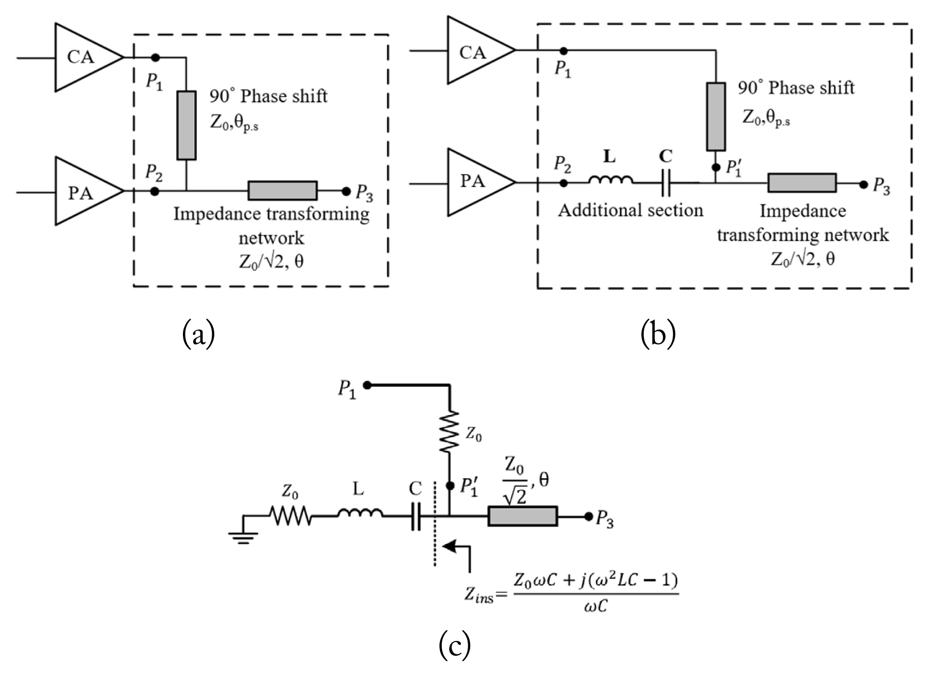
(a) Conventional Doherty combiner, (b) the proposed Doherty combiner I, and (c) the modified Doherty combiner I in Fig. 1(b).
In this paper, a new Doherty combiner is presented for improving bandwidth, not only magnitude, but also phase balance. The proposed combiners I and II were made up of series and parallel resonant circuits. The LC values in the proposed combiners were analyzed by deriving the slope of the phase differences and the reflection coefficient of the S-parameter.
II. The Proposed Doherty Combiner I with Series Resonator
The conventional Doherty combiner depicted in Fig. 1(a) consists of a carrier amplifier (CA) and a peaking amplifier (PA), as well as a phase shift and an impedance transforming network. The basic concept of the Doherty technique is that the CA is designed to saturate below the transition point (half of the maximum output voltage), and the PA commences linear operation, modulating the load of the CA from twice its optimum (2Ropt) to the optimum value (Ropt) [2]. The required load modulation method is achieved by using an impedance transforming network, which causes the limited bandwidth of the phase differences between S31 and S32. First, consider Fig. 1(b) for a wide phase balance. The series resonant circuit (L and C) at port 2 was added to the conventional Doherty combiner. Since the conventional Doherty’s phase slopes differ from S31 and S32, the phase differences vary as the frequency deviates from the central frequency [21]. The frequency deviations caused phase balance degradation. To improve the phase balance, we derived the design theory in a different way than in [22]. Instead of the derivative of phase differences, uniform phase balance was considered to set the targeted phase deviation. To analyze the proposed combiners, the output nodes of CA and PA were replaced by port 1 and port 2, respectively (i.e., input sources); however, port 3 was the output port for the combiner. Fig. 1(c) shows a modified diagram that illustrates the calculation of the phase differences S31 and S32 of the proposed combiner I in Fig. 1(b), terminating port 2 as port impedance Z0 and showing port impedance of P1 without a 90° phase shift. The input admittance looking at
To simplify the calculations, a 90° phase shift was added as a phase (θp.s) at the last step, as shown in Fig. 1(c). After terminating port 2 as the port impedance Z0, the ABCD parameters from node
where
From (2) and (3), S31′ and S32 are expressed in the Appendix. From S31′ and S32, the angular phases ∡S31′ and ∡S32 are described as (4) and (5) below.
where RR = ω2LC – 1.
Consider the 90° phase shift (θps) mentioned above. The phase differences (φdiff) of S31′ and S32 are expressed as φdiff = (θps + ∡S31′ ) – ∡S32. φdiff is calculated as the center frequency (f0) and lower band-edge frequency (f1) targeted half of the bandwidth, shown as (6)–(8).
If we set the f1 and φdiff, the upper band-edge frequency (
where ∡S32|θ=θn = θ32n, n = 1, 2.
The evaluation of tangent (α) is derived in (10) using trigonometric functions; this is done after replacing the left side of (9) with α,
where
where
Using (4) and (5), (11) can be derived as L and C, as in (12) and (13).
where
Therefore, the proposed Doherty output combiner I has the values of L and C, as in (12) and (13), after setting the phase differences S31 and S32 at the center frequency f0 and target frequency f1. This could be a more practical way to set the phase balance for target frequency.
III. The Proposed Doherty Combiner II with Series and Parallel Resonant Circuits
The L and C values obtained in Section II are juxtaposed with the targeted phase differences at the center frequency f0 and the specified band frequency f1. Thus, the phase slope of phase differences had a constant value in wideband. In this section, we consider the frequency bandwidth of the magnitude balance. The proposed Doherty combiner II has a series resonator and a parallel resonator, as shown in Fig. 2(a). The added parallel resonant circuit Lp and Cp only affected the magnitude bandwidth, which had a constant phase balance.

(a) The proposed Doherty combiner II using series and parallel resonant circuit and (b) the modified Doherty combiner II.
where
A = (Z0ω)2LpCs, B =Z 0 ωLp(ω2LsCs – 1),
C = 2Z0ω2CsLp – Z0(ω2LsCs – 1)(ω2LpCp – 1),
The input impedance Zin at port 3 can be obtained as (15) using (14). From (15), Zin can be rearranged (16).
where x = AC + BC, y = BC – AD, ω = C2 + D2.
The reflection coefficient (Γ) of S33 is given by (17) using (16). To determine wide magnitude bandwidth, the derivative of Γ with respect to ω is necessary, since (17) is a function of ω, Lp, and Cp.
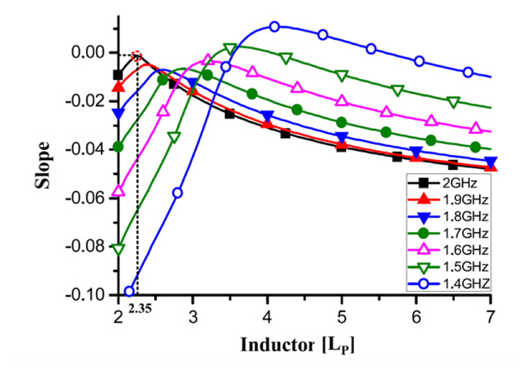
Fig. 3 shows plots of several graphs of the S33 slope versus Lp, varying from 2 to 7 nH and having a frequency range between 1.4 to 2 GHz generated using MATLAB. To obtain the Lp value for broad bandwidth, we observe that Lp = 2.35 nH is selected when the slope of
A simulated
IV. Simulation and Fabrication Results
1. Simulation Results Using Analysis Designer
To demonstrate the proposed design method, two proposed Doherty combiners (I and II) were designed using a central frequency of 2 GHz based on the algorithm below.
Draw the proposed Doherty combiner I and label its essential parameters (Z0, θps, L, and C).
Apply the circuit analysis on the ABCD parameter and S-parameter to obtain magnitude and phase terms, which are used to extract the required parameters when the θps = π/2 and resonant conditions are applied.
Express the phase differences (φdiff) of S31′ and S32 as φdiff = (θps + ∡S31′ ) – ∡S32. φdiff is set as the center frequency (f0) and lower band-edge frequency (f1), and calculate L and C.
Draw the proposed Doherty combiner II having Lp and Cp. Using the obtained value of L and C, derive the reflection coefficient of S33 at ports 1 and 2, which are terminated by a port impedance Z0.
Use MATLAB to calculate the derivative of S33 with respect to ω, and plot the S33 slope according to the Lp.
Perform circuit simulation and three-dimensional field analysis using ANSYS High-Frequency Structure Simulator (HFSS).
If the achieved results are desirable, then fabricate the proposed circuits to check the validity of the design theory.
This section describes circuit simulations conducted on the conventional Doherty combiner and the proposed Doherty combiners I and II. The inductor value L and capacitor value C was derived as 2.37 nH and 2.67 pF, respectively at f0 of 2 GHz, f1 of 1.9 GHz, and the phase difference of S31 and S32 was 1°. The values of the series resonant circuit of the proposed Doherty combiner II were also applied using the same value of the proposed combiner I. The values of the inductor (Lp) and capacitor (Cp) in the parallel resonant circuit are 2.35 nH and 2.69 pF, respectively, at zero slope.
Fig. 4(a) and 4(b) shows the S-parameter and phase differences of comparison simulation results according to the conventional and proposed Doherty combiners (I and II). The comparison simulations were conducted using ANSYS Designer. Since the target edge frequency f1 is 1.9 GHz and the phase balance is set as 1°; the circuit simulation results are consistent with the targeted results of the designed circuit. Magnitude bandwidth also increases 110 MHz bandwidth for the Doherty combiner II having a series and parallel resonator.

Comparison of the simulation results of conventional and proposed Doherty combiners: (a) S-parameter, (b) phase difference of S31 and S32, and (c) fabricated photos of the conventional, the proposed Doherty combiner I, and the proposed Doherty combiner II.
2. Fabrication Results and Measurements
Fig. 4(c) shows a fabricated photograph of the conventional circuit, proposed circuits I and II, from left to right. The fabricated substrate is Rogers RT5880, and the dielectric coefficient is 2.2. The chip inductor and capacitor used in this paper have a size of 2.0 mm × 1.2 mm. The line width of port impedance Z0 is 2.38 mm and the length is 27.4 mm.

Comparison results of (a) S-parameter and (b) phase difference.
V. Conclusion
In this paper, a novel Doherty combiner is proposed with the aim of extending bandwidth. The proposed Doherty combiners I and II consist of series or parallel resonators added to a conventional Doherty combiner. The proposed combiner I was derived by setting the targeted phase balance, and the series resonant values were obtained by setting the resonant condition as the phase balance. The proposed combiner II was calculated by obtaining the zero slope of the reflection coefficient of S33. The derived values of the proposed circuits were verified using the simulation and measured results. Both results show that the proposed combiner II has a wideband for not only magnitude bandwidth but also phase balance, with 25.9% and 112% improvement for magnitude and phase bandwidth, respectively, compared to the conventional Doherty combiner. Therefore, the proposed Doherty combiners can be applicable for wideband Doherty power amplifiers in baseband stations and various applications to balance of magnitude and phase characteristics.
Acknowledgments
This result was supported by “Regional Innovation Strategy (RIS)” through the National Research Foundation of Korea (NRF) funded by the Ministry of Education (MOE) (No. 2021RIS-004) and the Soonchunhyang University Research Fund.
Appendices
Appendix
S-parameters S31′ and S32 can be derived from the ABCD parameter in Fig. 1(c).
where
where
References
Biography

Youna Jang received her master’s degree in display engineering from Hanyang University, Seoul, Korea, in 2014. She also received her Ph.D. in electrical communication system engineering from Soonchunhyang University, Choongnam, Korea, in 2019. She designed as a designer of the RF filter in an internship program in 2015 at Qorvo, Bundang, South Korea. She was a lecturer at Soonchunhyang University from 2016 to 2020. She is currently a research professor at the Radio and Mechatronics Research Center at Soonchunhyang University. Her research areas include the design of passive components in microwave bands.

Cha Hye Seong received his B.E. degree in electrical engineering from Soonchunhyang University, Asan, Korea, in 2023. He received his master’s degree in ICT convergence at Soonchunhyang University. His current research interests include RF passive device theory, RF design, and RF testing. Currently, he is a member of the R&D center at SAWNICS.

Taehoon Kang was born in Incheon, Korea, in 1993. He received his M.S. degree from Soonchunhyang University, Asan, Korea, in 2019. Currently, he is accomplishing his Ph.D. at Soonchunhyang University. His current research interests include RF filter theory, design, and testing.

Sang-Min Han received his B.S., M.S., and Ph.D. degrees in radio sciences and engineering from Korea University, Seoul, Korea, in 1996, 1998, and 2003, respectively. From 1999 to 2001, he was a Lecturer with the School of Electrical Engineering, Korea University. From 2003 to 2004, he was a Post–Doctoral Research Fellow with the University of California at Los Angeles (UCLA), USA. From 2005 to 2007, he was a Senior Research Engineer with the Samsung Advanced Institute of Technology (SAIT), Korea. In 2007, he joined Soonchunhyang University, Korea where he is a professor with the Department of Information and Communication Engineering. He was a Visiting Research Faculty with the Georgia Institute of Technology (GT), Atlanta, USA from 2013 to 2014. Prof. Han is an Associate Editor of the Journal of the Korean Institute of Information Technology (JKIIT) and an Editorial Board Member of the Journal of Electromagnetic Engineering and Science (JEES). He has appeared in Marquis’ Who’s Who in Science and Engineering (2006–2007) and Marquis’ Who’s Who in Asia (2007). His research interests include RF/microwave system architectures with low-power/spectrum sensing, active integrated antennas, and reconfigurable RF systems/components.

Dal Ahn received his B.S., M.S., and Ph.D. degrees in electronics from Sogang University, Seoul, Korea, in 1984, 1986, and 1990, respectively. From 1990 to 1992, he worked with the Mobile Communications Division, Electronics, and Telecommunications Research Institute (ETRI), Daejeon, Korea. Since 1992, he has been affiliated with the Department of Electrical Engineering, Soonchunhyang University, Asan, Korea, where he is currently a professor. He is also currently the chief of the RF and Microwave Component Research Center (RAMREC) at Soonchunhyang University. In addition, he is a technical consultant for Tel Wave Inc., Suwon, Korea. His current research interests include the design and application of passive and active components at radio and microwave frequencies, the design of RF front-end modules for various handset systems using low-temperature co-fired ceramic (LTCC) technology, DGS circuit applications, and circuit modeling through a commercial EM analysis program. Prof. Ahn is also an editor of the Journal of Korea Electromagnetic Engineering Society and a senior member of the Korea Electromagnetic Engineering Society (KEES).