A Highly Efficient Broadband Class-E Power Amplifier with Nonlinear Shunt Capacitance
Article information
Abstract
A new approach to designing a broadband and highly efficient class-E power amplifier based on nonlinear shunt capacitance analysis is proposed. The nonlinear shunt capacitance method accurately extracts optimum class-E power amplifier parameters, including an external shunt capacitance and an output impedance, at different frequencies. The dependence of the former parameter on the frequency is considered to select an optimal value of external shunt capacitor. Then, upon determining the latter parameter, an output matching network is optimized to obtain the highest efficiency across the bandwidth of interest. An analytical approach is presented to design the broadband class-E power amplifier of a MOSFET transistor. The proposed method is experimentally verified by a 140–170 MHz class-E power amplifier design with maximum added power efficiency of 82% and output power of 34 dBm.
I. Introduction
A power amplifier (PA) is always an important component in a transmitting chain of a wireless system, since its performance strongly influences the overall system features, including bandwidth, output power, efficiency, and linearity. In a modern PA design, wide bandwidth and high efficiency are two major requirements that increase the number of frequency bands and reduce thermal problems in the power devices and their sizes and auxiliary costs. A switch-mode class-E PA with shunt capacitance is attractive for these purposes, due to its high efficiency and simple topology [1, 2]. However, [1] and [2] only concentrate on simplifying the analysis of the class-E PA while neglecting the actual characteristic of the shunt capacitance. In fact, the operation of the linear shunt capacitance class-E PA in theory is completely different from its practical operation. Because the parasitic drain-to-source capacitance of the switching device, which significantly contributes to the overall shunt capacitance in the operation, is nonlinear, it is necessary to take into account the nonlinear characteristics of this capacitance.
The theory of the class-E PA with a nonlinear capacitance was first published in Chudobiak’s work [3] in a case of the grading coefficient m = 0.5. Then several numerical analyses were performed with the grading coefficient m ≠ 0.5 [4, 5]. In these articles, only a nonlinear shunt capacitance of the power transistor is considered. Suetsugu and Kazimierczuk [6] has proposed an analysis and a design procedure for the class-E PA with a shunt capacitance composed of both transistor nonlinear output capacitance and linear external capacitance. This theory has been verified in a design of a high-efficiency class-E PA for 13.56 MHz wireless power transmission application [7]. The study of frequency limitation based on the nonlinear shunt capacitance theory has been presented in article [8], which showed the nonlinear dependence of frequency upon supply voltage, output power, and transistor characteristic. The performance as well as the topology of the class-E PA depends on the maximum frequency. An optimum performance is only addressed when the operating frequency does not exceed the maximum frequency. In the event that the operating frequency is lower than the maximum frequency, an added external shunt capacitor is necessary to obtain an optimal value of the shunt capacitor, as in the topology used in Suetsugu’s work, whereas the topology used by Chudobiak [3] is optimum if the operation and maximum frequencies are equal.
The mentioned studies concentrated on designing a class-E PA at a single frequency using an output resonant circuit with a high unloaded quality factor to tune the operating frequency. In the present work, a practical approach to designing a broadband high-efficiency class-E PA based on the nonlinear shunt capacitance theory is proposed. Applying nonlinear design equations from previous works [6, 8], the dependence of class-E PA operation on the frequency is focused on extracting the optimal values of the circuit parameters, including external shunt capacitance and output impedance. The topology of a low-pass matching network is utilized to overcome the restriction of the output resonant circuit for the broadband design. A prototype of a broadband class-E PA is implemented to validate the theoretical analysis.
II. Analyzing and Designing Broadband Class-E PA
A conventional circuit of the MOSFET class-E PA with shunt capacitance is illustrated in Fig. 1(a). Without an input driving signal, a DC-voltage VGS is applied to the gate of the transistor to turn the transistor off. A DC-supply voltage VDD connects to the drain of the transistor through the choke coil LRFC with the only purpose of supplying DC power to the transistor. A shunt capacitor Cp, in parallel with the transistor, keeps a sinusoidal current waveform to alternate flow between the transistor and the shunt capacitor Cp. In common, Cp, consisting of a nonlinear shunt capacitance of a transistor Cds and a linear external capacitance Ce, is described as follows:
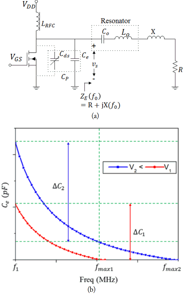
The MOSFET class-E PA with shunt capacitance. (a) Conventional topology. (b) Ce versus f0 for selected VDD.
where Cj0 is the shunt capacitance at the drain-to-source voltage vs = 0 V, and Vbi is the built-in potential of the MOSFET body diode. A series-resonant C0L0 circuit tunes to the fundamental frequency with a high unloaded quality factor Q to shape the output current to be sinusoidal at the fundamental frequency. At the fundamental frequency f0, a load ZE is inductive, as shown in Fig. 1(a). An optimal value of ZE guarantees that there is no overlap between the transient drain current and the voltage.
In previous works [6, 8], the design equations expressed the relationship among the operating frequency f0, the supply voltage VDD, the output power Po, the external linear capacitance Ce, and the characteristic parameters of MOSFET, Cj0, Vbi. The numerical solutions, a set of tables and figures, illustrate that relationship. For the purpose of broadband design, this work gives a practical scenario in which a specification of class-E PA is defined as containing the operating frequencies, the output power, and the model of the MOFET transistor. Based on this specification, the analysis concentrates on the dependence of the circuit parameters on the operating frequency and the DC-supply voltage. For selected values of output power Po and MOSFET transistor parameters Cj0, Vbi, and for swept values of operating frequency f0 and DC-supply voltage VDD, this work re-solves the nonlinear design equation to extract the values of external linear capacitance Ce and fundamental load ZE. Then the optimal values of these parameters are chosen to obtain the highest efficiency of class-E PA.
1. Selecting VDD to Obtain the Actual Value of Ce
Fig. 1(b) plots the linear external Ce as a function of the operating frequency f0 and the DC-supply voltage VDD. Ce = 0 at the maximum operating frequency fmax. To obtain high efficiency for a broadband design, the upper frequency fU of the bandwidth should be less than or equal to fmax. At the same conditions of Po and transistor, the increased VDD results in the decrement of fmax. The theory of the maximum frequency of class-E PA with the nonlinear shunt capacitance expressing the relation between the maximum frequency and the supply voltage was presented in detail in another work [8].
In the broadband design, the optimum external capacitance varies with the frequency. Unfortunately, the actual value of the external capacitor is a constant; therefore, the optimum state is unattainable at every frequency. Simply, the actual Ce is chosen as the average value of the optimum Ce. To approximate the idealized class-E PA mode, the deviations of the actual Ce from the design values, depending on the variation of the optimum Ce with the f0, should be minimized. The small variation can result in the decreased level of the deviation. As shown in Fig. 1(b), at a given specification, the variation at a low band is much greater than that at a high band, whereas, at a given frequency band, from f1 to fmax1, the variation will be smaller in the case of a high voltage, ΔC2 > ΔC1. Hence, combined with the maximum frequency condition as mentioned above, V1 corresponding to fmax1 is the optimal supply voltage with a bandwidth of f1 to fmax1.
2. Output Matching Network
For most practical applications, it is necessary to match the required class-E PA optimum load impedance ZE with a standard load resistance RL. In broadband design, the conventional topology of a class-E power amplifier is not proper for obtaining broadband design, due to the limitation of the series resonator, which requires a high Q factor to perfectly prevent harmonic frequency.
Low-pass matching networks (LMNs), one of the common ways of designing broadband class-E PAs, have shown high performance in published papers [1, 2]. The LMN has two functions of low-pass filter, as a function of a resonant circuit and a matching network. Since a higher order of low-pass filter leads to wider bandwidth and steeper stopband attenuation, by increasing the value of the order, the LMN can overcome the bandwidth limitation of the resonator. However, the tradeoff between performance and the size of the low-pass filter, which depends on the requirements of the specifications, should be considered. The LMN also makes the circuit simpler by substituting both for the resonator and the output matching network in the conventional topology of a class-E PA.
The efficiency of an LMN depends on the accuracy in extracting ZE. In the conventional method [1, 9, 10], ZE is expressed as follows:
This expression was set up with the assumption that the linear shunt capacitance is inaccurate for application to MOSFET devices. As shown in Fig. 1(a), the resonant circuit, representing a short and an open circuit at the fundamental and harmonic frequencies, respectively, has zero reactance at the fundamental frequency; therefore, ZE is expressed by a fundamental inductive load that consists of R and X in series:
where φ1 is the phase of vs. Because the reactance of the resonator is zero at the operating frequency, the relation between φ1 and vs is described by:
Hence, the optimal load impedance is
While R is only a function of VDD and Po, X depends on VDD, Po, f0, and the characteristic of the transistor, different from the conventional formula. Similar to the method of extraction of Ce, the MATLAB program is composed to solve the nonlinear equation of X. Due to the dependence of the output impedance on the frequency, the LMN is required to match the various ZE to the standard load. The simple method to design the various output impedance LMNs is to use the Impedance Matching Utility Tool of the Advanced Design System (ADS).
3. Design Procedure
From the above analysis, the design steps of the broadband class-E PA are summarized as follows:
Based on specifications of the operating frequencies and expected output power, select the type of transistor.
Using the MATLAB program to solve the nonlinear de sign equations, plot Ce as a function of f0 and VDD, as shown in Fig. 1(b).
Select VDD to obtain the actual value of Ce. The rule of VDD selection is as follows: supposing the bandwidth of design class-E PA from f1 to f2, the optimal VDD has a value whose corresponding maximum frequency fmax is equal to f2. Then, the actual value of Ce is chosen as an average value of the optimal Ce at every frequency of bandwidth.
Use Eqs. (5)–(6) to extract ZE. Select the order of LMN based on the specification of bandwidth. Synthesize LMN by using the Impedance Matching Utility Tool of ADS.
III. Simulation and Experiment Results
To verify the above analysis, a prototype of class-E PA circuit was designed for public and homelands security application with Po of 34 dBm over a bandwidth of 140–170 MHz. The MOSFET used in this design was MRF282SR1, with Cj0 described by the following:
where Coss and Crss, respectively, are the output and reverse transfer capacitances of the transistor, (often provided in catalogs by power MOSFET manufacturers), and Vspec is a special value of supply voltage used to measure the values of Coss and Crss. Using MATLAB, the Ce as a function of f0 for selected values of VDD was plotted in Fig. 2. From Fig. 2, the actual VDD and Ce were 8 V and 1.2 pF, respectively. Eqs. (5)–(6) were solved using MATLAB to determine the output impedance at various frequencies. Fig. 3 plots the output impedance versus the operating frequency. By setting the output impedances at corresponding frequencies, the ADS Impedance Matching Tool synthesized the matching network. A three-stage LMN with a bandwidth of 20% was extracted, illustrated in Fig. 4. The simulated drain minimized power dissipation on the transistor. A voltage and current waveforms depicted in Fig. 5 under the optimum operation slightly overlap, resulting in a prototype of class-E PA circuit was realized on a Taconic TLC PCB material with a thickness of 0.787 mm and a dielectric constant of 3.2. A photograph of the prototype is shown in Fig. 6. The output power was measured using an Agilent 85665EC spectrum analyzer with a maximum measurement output of 30 dBm. An attenuator of − 39.67 dB was added at the end of the circuit. The PAE and output power versus the frequency and input power were plotted in Fig. 7. The lumped components are available only in discrete values provided by the manufacturers, which is the main reason for the differences between the simulated and measured results. A summary of the experimental results compared with other articles on high efficiency proving this method’s advantages is shown in Table 1.
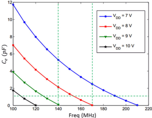
Determining the optimal VDD and Ce.

Fundamental output impedance.
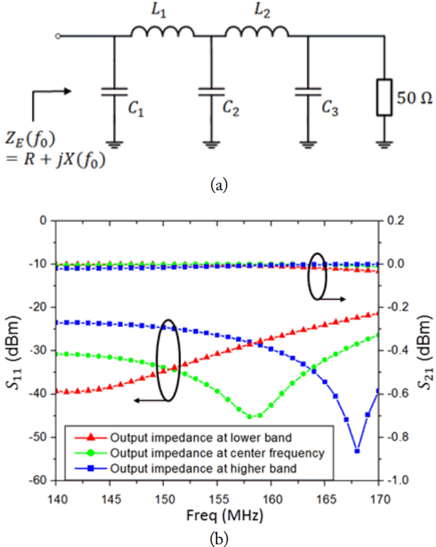
The low-pass matching network. (a) Schematic. (b) S-pa-ameters at different output impedance.
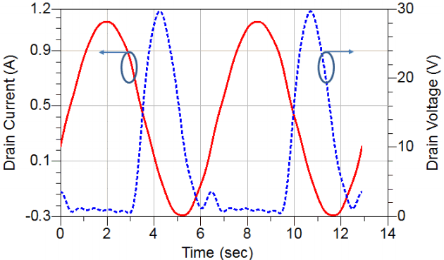
Drain current and voltage simulation waveform of class-E PA circuit.
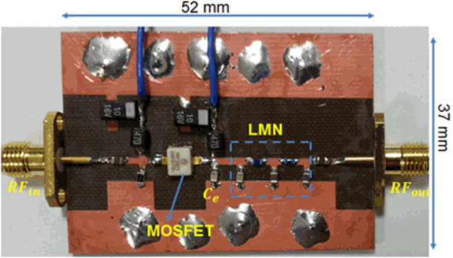
Photograph of fabricated MOSFET class-E PA.
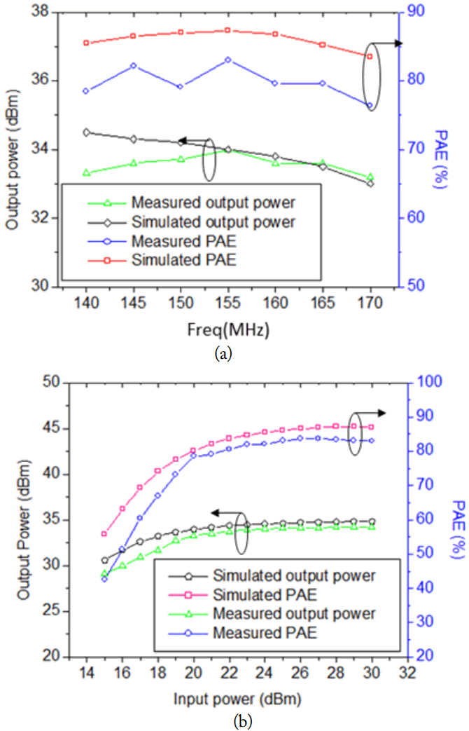
Simulated and measured results. (a) Po and PAE versus f0. (b) Po and PAE versus Pin.
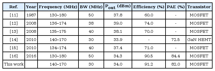
Comparative results
IV. Conclusion
This work presented a practical method to implement a high-efficiency broadband class-E PA using a MOSFET transistor with nonlinear output capacitance. The extraction of the shunt capacitance and the fundamental output impedance via numerical analysis was the principal step in this article. The peak PAE of 82% and the average PAE of 80% with the output power level of 34 dBm at frequencies from 140 MHz to 170 MHz were experimental results that validated the accuracy of this method. Two of the most outstanding advantages of the class-E power amplifier with shunt capacitance as high efficiency and simple topology were shown in this work.
Acknowledgements
This work was supported by a grant-in-aid of Hanwha Systems.
References
Biography

Ninh Dang-Duy
received his B.S. degree from the School of Electronics and Telecommunications at Hanoi University of Science and Technology, Hanoi, Vietnam in 2013. He is currently pursuing an Integrated Master’s Ph.D. degree in the Department of Information Communication, Materials, and Chemistry Convergence Technology at Soongsil University, Seoul, Korea. His current research interests are power amplifiers, metamaterials, and wireless power transfer.

Nam Ha-Van
received his B.S. degree from the School of Electronics and Telecommunications at Hanoi University of Science and Technology, Hanoi, Vietnam in 2012. He is currently pursuing an Integrated Master’s Ph.D. degree in the Department of Information Communication, Materials, and Chemistry Convergence Technology at Soongsil University, Seoul, Korea. His current research interests are wireless power transfer, wireless power transfer for biomedical implants, metamaterials, power amplifiers, dual-band RFID antenna, and phased array antennas.

Daesik Jeong
received the B.S. degree in electric wave engineering from Korea Maritime and Ocean University, Pusan, Korea, in 2005, and the M.S. degree in electronic engineering from Kyungpook National University, Daegu, Korea, in 2007. He was worked Hanwha Systems. His research interests include phased array antenna design and radar system.

Dong Hwan Kim
received the B.S. degree in electronic engineering from Inje University, Gimhae, Korea, in 2005, and the M.S. degree in electronic engineering from Kyungpook National University, Daegu, Korea, in 2007. He is currently working at Hanwha Systems. His research interests include active phased array antenna design and multi-function radar system.

Chulhun Seo (M’97–SM’14)
received B.S., M.S., and Ph.D. degrees from Seoul National University, Seoul, Korea, in 1983, 1985, and 1993, respectively. From 1993 to 1995, he was with the Massachusetts Institute of Technology (MIT), Cambridge, MA, USA, as a Technical Staff Member. From 1993 to 1997, he was with Soongsil University, Seoul, Korea, as an assistant professor. From 1999 to 2001, he was with MIT as a visiting professor. From 1997 to 2004, he was with Soongsil University as an associate professor. Since 2004, he has been a professor of electronic engineering with Soongsil University. He was IEEE MTT Korea Chapter chairman from 2011 to 2014. He is the president of the Korean Institute of Electromagnetic Engineering and Science (KIEES) and Dean of Information and Telecommunications College at Soongsil University. He is the director of the Wireless Power Transfer Research Center, supported by the Korean government’s Ministry of Trade, Industry and Energy, and the director of the Metamaterials Research Center, supported by Basic Research Laboratories (BRL) through an NRF grant funded by the MSIP. He is the director of the Center for Intelligent Biomedical Wireless Power Transfer supported by the National Research Foundation of Korea (NRF) grant funded by the MSIP. His research interests include wireless technologies, RF power amplifiers, and wireless power transfer using metamaterials.