


I. Introduction
Microwave low-noise amplifiers are widely used in transceiver modules for military and civilian radar and communication systems. Notably, low-noise amplifiers in military systems must withstand high power and possess low-noise characteristics over a wide frequency range. To meet these requirements, low-noise amplifiers using GaN high electron mobility transistors (HEMTs) on SiC, which have a higher breakdown voltage, higher electron velocity, and better thermal conductivity than Si or GaAs devices, have been extensively researched [1, 2]. While GaAs pseudomorphic HEMTs (pHEMTs), characterized by low operating voltage, high electron mobility, and high maximum operating frequency, are actively used in transceiver modules, they require the application of additional limiters to block leaked power from the transmitter and to protect the receiver circuit from unwanted high-input power, which adversely affects both the size reduction of the module and the necessary low-noise performance. This drawback has contributed to a recent research trend focused on using GaN HEMTs on SiC in the receiver module [3–8].
This study designs and fabricates a GaN low-noise amplifier monolithic microwave integrated circuit (MMIC) for a Ku-band RF transceiver module. To achieve this, a 0.2 μm GaN HEMT on SiC obtained from the Electronics and Telecommunications Research Institute (ETRI) was utilized, while the transistor was stabilized using the source feedback technique by adding an inductor to the source of the transistor. This allowed for a favorable impedance trajectory marked by high-gain matching and low-noise matching [9, 10]. However, while the source inductance improved the stability of the transistor, it also degraded the available gain and noise figure. As a result, this study chose to focus on the optimal inductance for the target frequency region to minimize gain reduction and alleviate the difficulty involved in impedance matching. Therefore, this paper presents the design and measurement results of a Ku-band, highly robust GaN low-noise amplifier MMIC equipped with a source feedback inductance fabricated using the 0.2 μm GaN HEMT process presented by ETRI.
II. Circuit Design
1. The 0.2 μm GaN HEMT
The GaN HEMT on SiC utilized in this study featured a gate length of 0.2 μm, and a gate width of 4 μm × 50 μm, and could operate up to 26 GHz. Considering the bias conditions of VDS = 20 V and IDS = 20 mA, the maximum available gain (MAG) and minimum noise figure at 50 Ω in the Ku-band (15–16 GHz) of the destabilized transistor were expected to be 12.41–12.67 dB and 1.85–1.99 dB, respectively. The extrapolated transistor cutoff frequency fT and maximum oscillation frequency fmax at the bias point were 31.7 GHz and 70.3 GHz, respectively. Furthermore, the 2 μm × 100 μm test transistor used for process control monitoring had a breakdown voltage of more than 170 V and a maximum gate-to-source voltage of 0 V.
For low-noise amplification, the 4 μm × 50 μm and 4 μm × 100 μm GaN HEMTs were available from ETRI. Since the former offered a better noise figure by about 0.2 dB in the Ku-band than the latter, the 4 μm × 50 μm transistor was chosen as the amplifying device in this study, despite the 2 dB MAG reduction.
The design specifications of the proposed low-noise amplifier MMIC had to ensure attaining a linear gain of 15 dB or more and a noise figure of 2.8 dB or less, as shown in Table 1. Notably, the capacitor in the circuit design was replaced with an equivalent circuit model extracted from the measured data, while the inductor and other matching elements were modeled using Keysight ADS 2.5D electromagnetic momentum simulations.
The S-parameter data at VDS = 20 V and IDS = 20 mA indicated that the transistor was unstable in the Ku-band. Before proceeding with the gain and noise simulation, the stable operation of the transistor had to be secured. Therefore, for transistor stabilization, an inductive component was added to the source of the transistor by inserting a microstrip line between the transistor source and the ground, as shown in Fig. 1. Notably, a microstrip line inductor was utilized, as it was found to be more effective in the Ku-band than loop or spiral inductors with regard to self-resonance and size reduction.
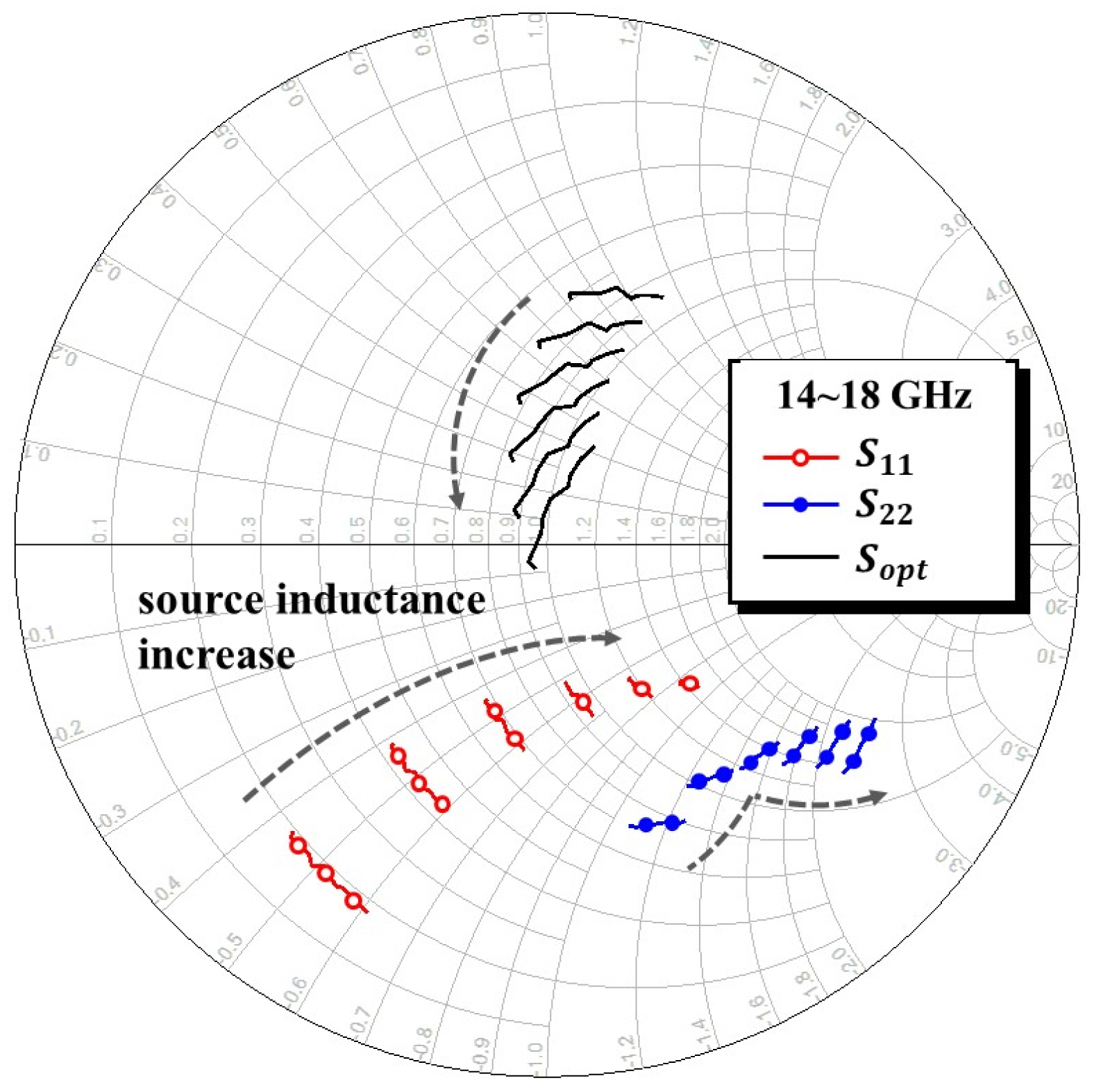
Fig. 2 depicts the variations in the MAG, the noise figure at 50 Ω, and the stability factor (K), while Fig. 3 presents the changes in the input/output reflection coefficients and optimal noise impedance in the Ku-band with an increase in the source inductance up to 1.5 nH. It is evident that with an increase in source inductance in the Ku-band, the stability factor K improved, but the noise figure at 50 Ω decreased, owing to the fact that the optimum noise source impedance had approached 50 Ω. The MAG was observed to be slightly reduced as well. This indicates that with proper source inductance, an impedance trajectory that balances the overall performance of stability, gain, and noise figure while minimizing the required number of passive elements in the matching circuit can be obtained. In this study, the microstrip lines used in all three stages of the designed amplifier had a line width of 25 μm and a length of 200 μm, which is equivalent to an inductance of approximately 1.4 nH, including a via-hole inductance.
2. Matching Circuit
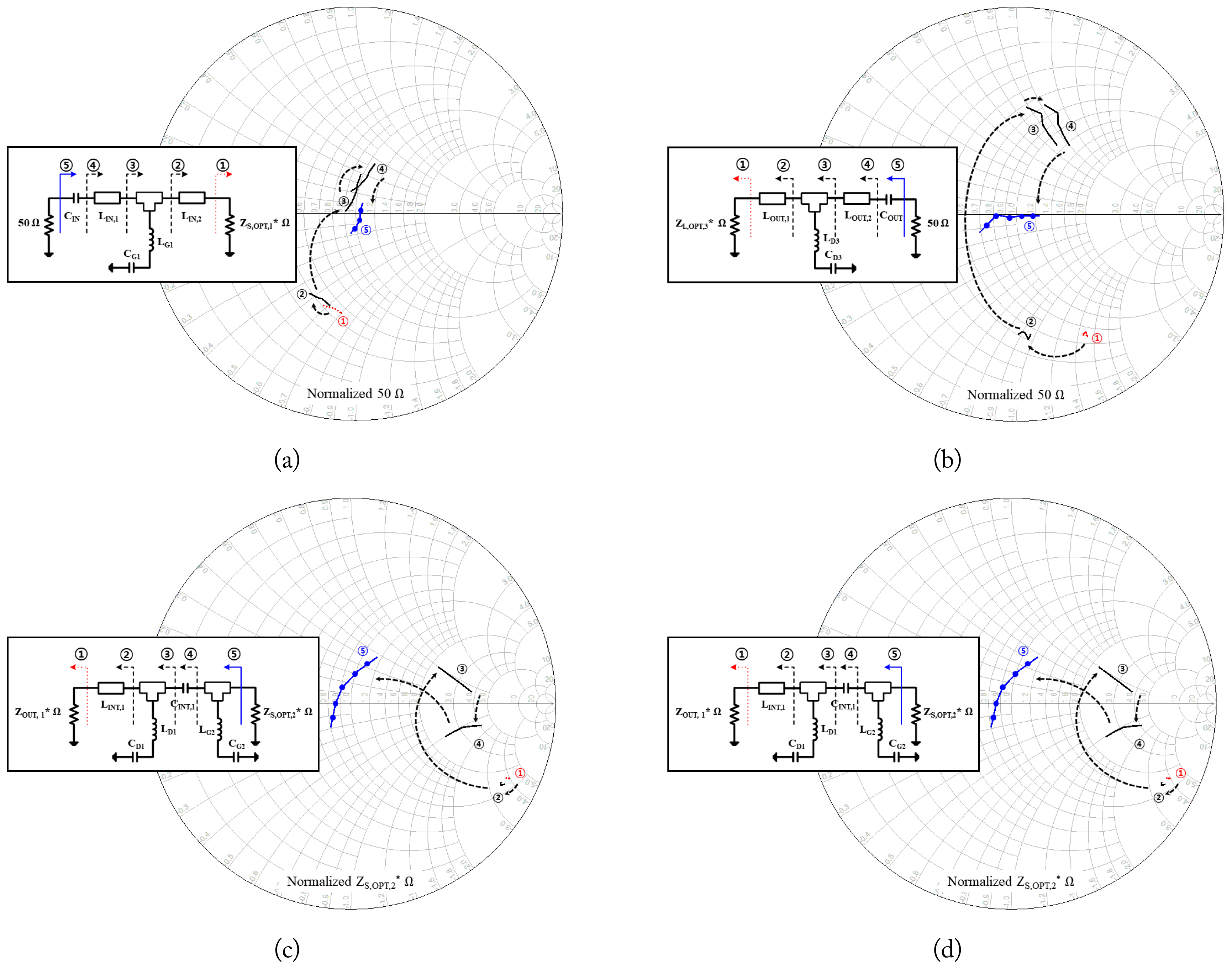
Fig. 1 illustrates the gain circle and noise circle at 16 GHz, including the impedance trajectories for the optimal gain and minimum noise figure between the 14–18 GHz frequency band, on inserting the microstrip line into the transistor source.
The optimal gain impedance (ZS,Gain) and noise source impedance (ZS,NF) at 16 GHz were 11.51 + j23.09 Ω and 40.72 + j37.50 Ω, respectively. The corresponding gain and noise figure achieved with ZS,Gain were 9.66 dB and 2.37 dB, while those achieved with ZS,NF were 8.18 dB and 1.37 dB, respectively. Subsequently, the compromised optimal source impedance (ZS,OPT = 20.3 + j26.4 Ω) and load impedance (ZL,OPT = 36.0 + j74.8 Ω) were selected to balance the gain and noise figure. The expected gain and noise figure at these impedance conditions were approximately 9.4 dB and 1.7 dB, respectively.
To obtain a high gain, the proposed Ku-band low-noise amplifier was designed based on a three-stage cascaded common-source configuration, the schematic circuit diagram for which is depicted in Fig. 4. The same bias conditions were applied to each stage, while a gate bias voltage was shared through 250 Ω gate resistors and bypass capacitors to ensure stability. Furthermore, RF choke inductors and resistor-capacitor shunt trap circuits were inserted into the drain bias circuit to suppress low-frequency oscillation, and 2.5 Ω series resistors were employed to connect the drain bias and prevent additional loop feedback [10, 11].
Fig. 5 shows the impedance trajectories of the input, output, and inter-stage matching circuits on a Smith chart. The input and output matching circuits managed to move the complex conjugate source impedance (ZS,OPT,1*) of the first-stage transistor to 50 Ω and the complex conjugate load impedance (ZL,OPT,3*) of the third-stage transistor to 50 Ω, respectively. Subsequently, when the input matching circuit was connected to the first-stage transistor, the inter-stage matching circuit between the first and second stages moved the output impedance (ZOUT,1) of the first transistor to the complex source impedance (ZS,OPT,2) of the second-stage transistor. Furthermore, when the input matching circuit and inter-stage matching circuit between the first and second stages were applied to each stage, the inter-stage matching circuit between the second and third stages moved the output impedance (ZOUT,2) of the second transistor to the complex source impedance (ZS,OPT,3) of the third-stage transistor. Finally, the matching circuit design was completed by fine-tuning the circuit performance.
Fig. 6 shows a photograph of the fabricated Ku-band GaN HEMT low-noise amplifier MMIC, which occupied an area of 1.66 mm × 1.16 mm. The MMIC chip was attached to an aluminum carrier using a silver epoxy process for on-wafer measurement.
III. Measurement
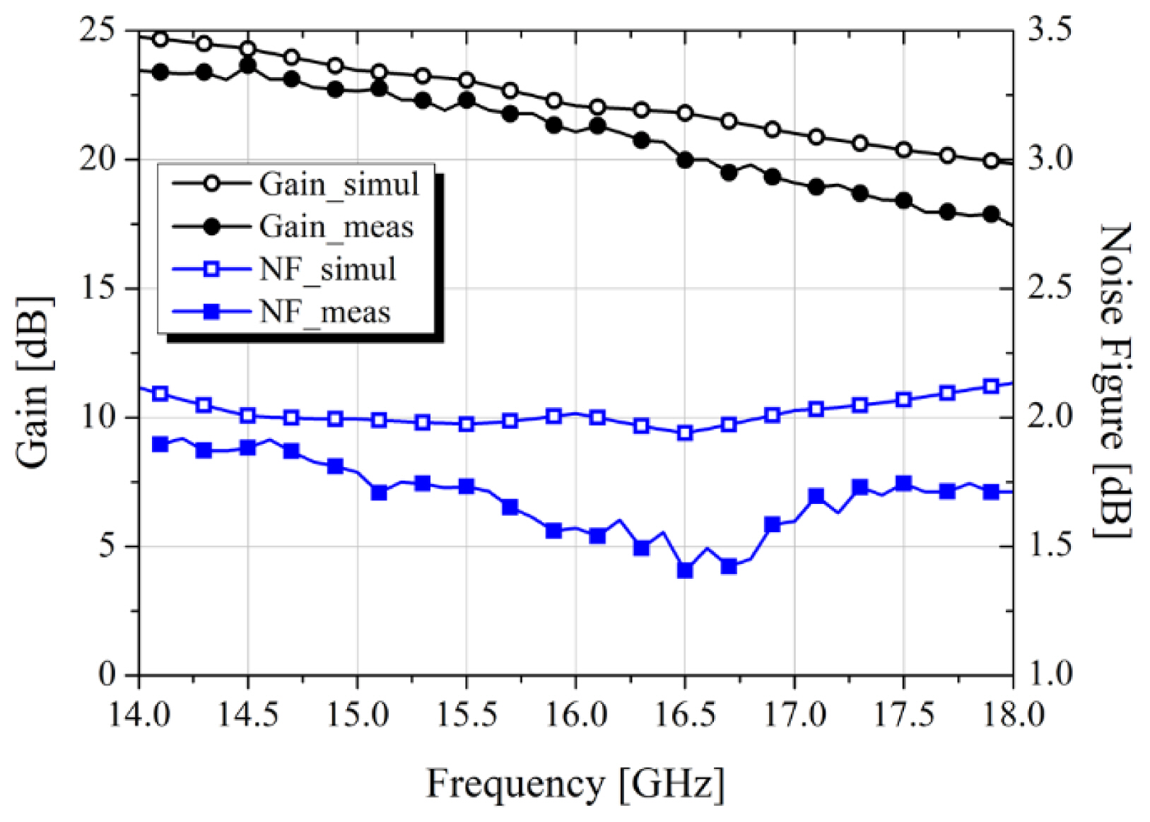
Figs. 7 and 8 display the S-parameter and noise measurement results of the low-noise amplifier MMIC under the bias conditions of VDS = 20 V and IDS = 84 mA, respectively. The S-parameter measurement was performed using the cascade on-wafer probe system and the Keysight network analyzer (N5230A). Meanwhile, for noise measurement, the noise source (N4002A) and Keysight signal analyzer (N9030B) were employed. The input return loss S11 was measured to be 19.6–21 dB and the output return loss S22 was 9–12 dB in the frequency range of 15–16 GHz. Compared to the simulation results in the target frequency band, S11 exhibited an improvement of about 5 dB while S22 degraded by about 10 dB. The gain in the target frequency band was 21.3–22.6 dB, indicating a 1-dB reduction in gain on using the proposed amplifier MMIC, while the noise figure was 1.7–1.8 dB, which was a 0.4 dB improvement over the simulated results.
Fig. 9 shows the measurement analysis results of the Ku-band low-noise amplifier MMIC. The circles in the figure represent the gain circles for a contour step of 0.1 dB and noise circles for a contour step of 0.2 dB in the 4 × 50 μm transistor at 16 GHz. The figure is an enlarged version of Fig. 1, with the designed input matching impedance (ZIN,TR1,SIMUL*) and estimated input matching impedance (ZIN,TR1,MEAS*) obtained from the measurement of the first-stage transistor simultaneously plotted on it. To explain the difference between the designed and estimated input matching impedance results, a capacitance change of about 10% was assumed due to the process variation, while the 2.5D electromagnetic simulation results were considered for other passive components. Furthermore, owing to an increase in the primary capacitance of the equivalent capacitor model, the debugging impedance trajectory (ZIN,TR1,DEBUG*) was found to be similar to the actual measured results. At an impedance of ZIN,TR1, DEBUG*, the gain degraded by about 0.8 dB and the noise figure improved by about 0.4 dB. Notably, the discrepancy between the simulated and measured results can be partly explained by variations in the dielectric deposition process that result in an impedance shift toward a region of better noise and poorer gain.
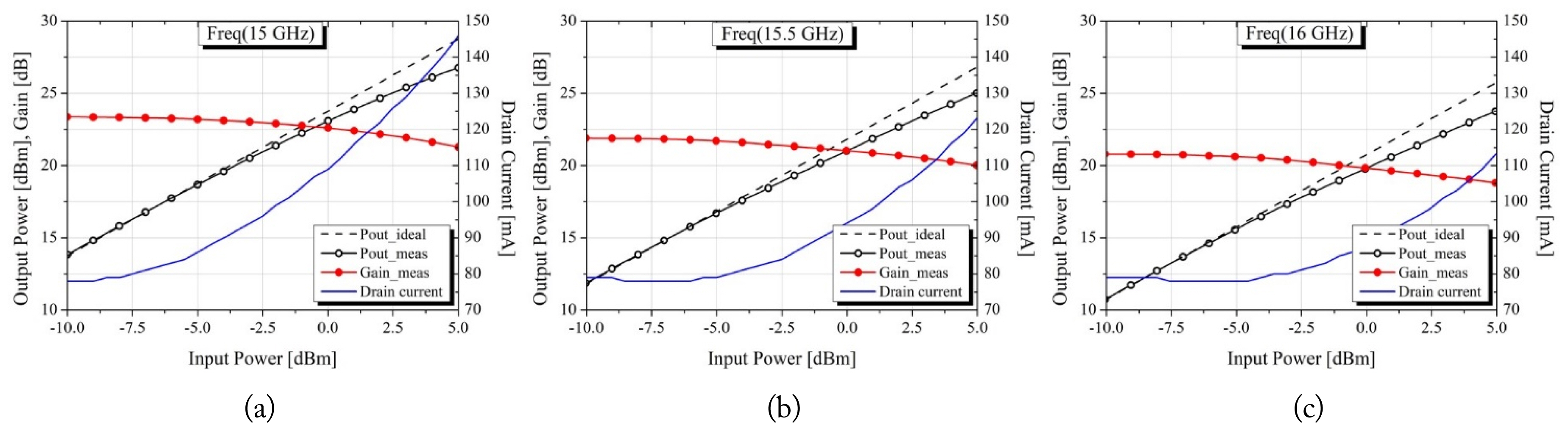
Fig. 10 presents changes in output power and power gain as functions of the input power at 15, 15.5, and 16 GHz under bias conditions of VDS = 20 V and IDS = 84 mA. At 15 GHz, the output 1-dB compression point (P1dB) was measured to be 24.3 dBm at an input power of 1.5 dBm. Furthermore, according to the results of a full power test, the fabricated amplifier could endure an input power of about 7 dBm, which corresponds to an approximate compression point of 4.5 dB. However, when the input power exceeded 7 dBm, the power test identified the occurrence of gain degradation. Notably, the power-handling capability of the proposed amplifier could be improved to some extent by increasing the device size in the final amplifying stage. Fig. 11 depicts the measured results of the third-order intermodulation distortion product (IMD3) at 15, 15.5, and 16 GHz when two-tone signals with a frequency interval of 50 MHz were applied to the proposed low-noise amplifier MMIC [12]. The input third-order intercept point (IIP3), estimated from the IMD3 component with fLow = 15.05 GHz, fHigh = 15.1 GHz, and 2fLow − fHigh = 15 GHz, was 8.1 dBm, while the output third-order intercept point (OIP3) was 33.3 dBm.
Table 2 lists the measured P1dB, power gain, and IIP3 characteristics of the low-noise amplifier MMIC within the 15–16 GHz frequency range, with the output P1dB being more than 20 dBm and IIP3 measured at 5.8–10.1 dBm. Table 3 compares the results of this study with those of other published low-noise amplifier MMICs using GaAs or GaN HEMTs, establishing that the fabricated Ku-band GaN HEMT low-noise amplifier MMIC delivers excellent performance in terms of noise, circuit compactness, and power robustness [13–20].
IV. Conclusion
This study designed, fabricated, and evaluated a Ku-band GaN low-noise amplifier MMIC using ETRI’s 0.2 μm GaN HEMT on SiC process. A source degeneration inductance was inserted into the transistor to induce the feedback effect required to improve stability and optimize the design impedance. It also allowed for the use of simple matching circuits and minimized chip size. The fabricated low-noise amplifier MMIC exhibited a linear gain of 21.3–22.6 dB, a noise figure of 1.7–1.8 dB, an input return loss of 19.6–21 dB, an output P1dB of more than 20 dBm, and an output IP3 of approximately 27.6–33.3 dBm in the 15–16 GHz frequency range. These results indicate that the low-noise amplifier MMIC proposed in this work has the potential to play a pivotal role in the development of Ku-band military radar transceiver modules that simultaneously require high-input power endurance and low-noise performance.