Analysis of the Interference Effects in CMOS Image Sensors Caused by Strong Electromagnetic Pulses
Article information

Abstract
With the electromagnetic environment becoming increasingly complex, it is crucial to address the risk posed by electromagnetic pulse, which critically impairs the performance and reliability of electronic systems based on complementary metal oxide semiconductor (CMOS) image sensors. In this context, research on the failure types of CMOS image sensors in a high-power electromagnetic environment, caused by strong electromagnetic pulses and the rapid evaluation method of interference immunity, has garnered significant interest. This paper conducts electromagnetic pulse simulation experiments on CMOS image sensors to first study their failure types, such as image abnormalities and functional interruption, and then identify the corresponding failure criteria. Furthermore, this study builds on the small sample test evaluation method to investigate the interference threshold of functional interruptions in CMOS image sensors by calculating the failure probability at different field strengths. The obtained data were combined with the Weibull distribution function for fitting, the results of which found the interference threshold to be at 40.4 kV/m. The findings of this study provide a basis for evaluating the survivability of CMOS image sensors and their associated reinforcement technology in high-power electromagnetic environments.
I. Introduction
A complementary metal oxide semiconductor (CMOS) image sensor (CIS) is a typical solid-state imaging sensor consisting of several modules, such as pixel arrays, signal processing circuits, analog-to-digital (AD) conversion circuits, and controllers. Its unique advantages include low cost, small size, high integration, low power consumption, simple control, and fast readout. As a result, it is widely used in imaging devices meant for visual surveillance, medical imaging, automotive electronics, and other visible light imaging fields [1–3].
However, in some specific environments, such as medical systems, the nuclear industry, and high-energy physical test conditions, irradiating high-dose-rate X-rays or γ-rays create a complex, intensive electromagnetic field environment in the local area. Peak field strengths in such environments are typically found to be significantly greater than 100 V/m. According to the international standard IEC 61000-2-15 [4], this represents a high-power electromagnetic (HPEM) environment, which is much harsher than conventional electromagnetic compatibility (EMC) testing environments. Notably, the monitoring and diagnostic imaging equipment operating in such an environment often encounters functional failures, performance degradation, interference, and damage to electrical and electronic systems [5–8]. Therefore, it is crucial to research the electromagnetic pulse (EMP) effects of CIS in HPEM environmental conditions to not only identify their failure types and interference thresholds but also establish a basis for application evaluation and robustness.
In recent years, studies on the effects of EMP on imaging devices have primarily focused on reports on failure types, methods for determining interference thresholds, and some reinforcement methods [9–15]. For instance, in 2012, Schwarz et al. [11] from Tel Aviv University studied the failure types and degradation of CMOS cameras under electromagnetic interference to identify perturbations in the images appearing in CMOS image sensors. Notably, with regard to the interference threshold of EMP, most experimental analyses and evaluations have used small sample tests due to the high cost involved. In 2018, Zhang et al. [13] of Nanjing University of Technology studied the EMP effect on unmanned aerial vehicle image transmission systems. They identified two types of failure—image destruction and signal loss—and obtained an interference field strength threshold of 15.6 kV/m based on the small sample test method. In 2019, Wu et al. [14] of Tsinghua University conducted an experimental study involving commercial imaging equipment in an HPEM environment. Effects such as abnormal functioning of imaging devices, degradation of imaging quality, and even burning of port components were observed. In addition, the researchers proposed the concept of a probability threshold to assess the failure of devices by assigning a weighting factor.
In summary, although the existing research has successfully detected a few failure types observable in CIS in the HPEM environment, their corresponding descriptions and classifications have yet to be determined. Moreover, due to the randomness of coupling paths and instability of the pulse source, which contributes to the failure probability of a device under different field strengths, the reliability of the traditional small sample method for assessing the interference threshold is poor. In this paper, a transversal electromagnetic wave (TEM) chamber irradiation test is conducted for CIS to first identify its failure types in the HPEM environment and then describe and analyze them in detail. Furthermore, to address the problem of the poor reliability of the interference threshold, this paper builds on the small sample method by increasing the number of tests conducted within the permitted range to obtain the failure probability of different field strength intervals. Subsequently, these results are utilized to characterize the anti-interference capability of the device. Finally, by combining the failure probabilities with the small sample evaluation method, the interference threshold of the device is determined and verified. Notably, this is the first study to propose a rapid assessment method—identification of failure type to failure probability to failure threshold—for the anti-interference capability of complex systems under an HPEM environment. Moreover, the research results provide basic data and technical support for assessing the survivability of CIS under HPEM environments and for building its reinforcement technology.
II. Experiment Description
The test sample considered in this study was a commercial CIS chip based on a 4-T pinned photodiode (PPD) image structure. It used the rolling shutter exposure mode, with a resolution of 2.1 million pixels and an image element size of 3 μm × 3 μm [16]. Fig. 1 presents a block diagram of the selected CIS, whose readout circuit includes the analog front-end, the addressing circuit, serial peripheral interface (SPI) registers, and a low-voltage differential signaling (LVDS) block. The CIS image output was selected in 8-bit mode, with a maximum gray value of 255 digital number (DN). The irradiated plate and laboratory conditions met the relevant standards of the EMP test [17, 18].
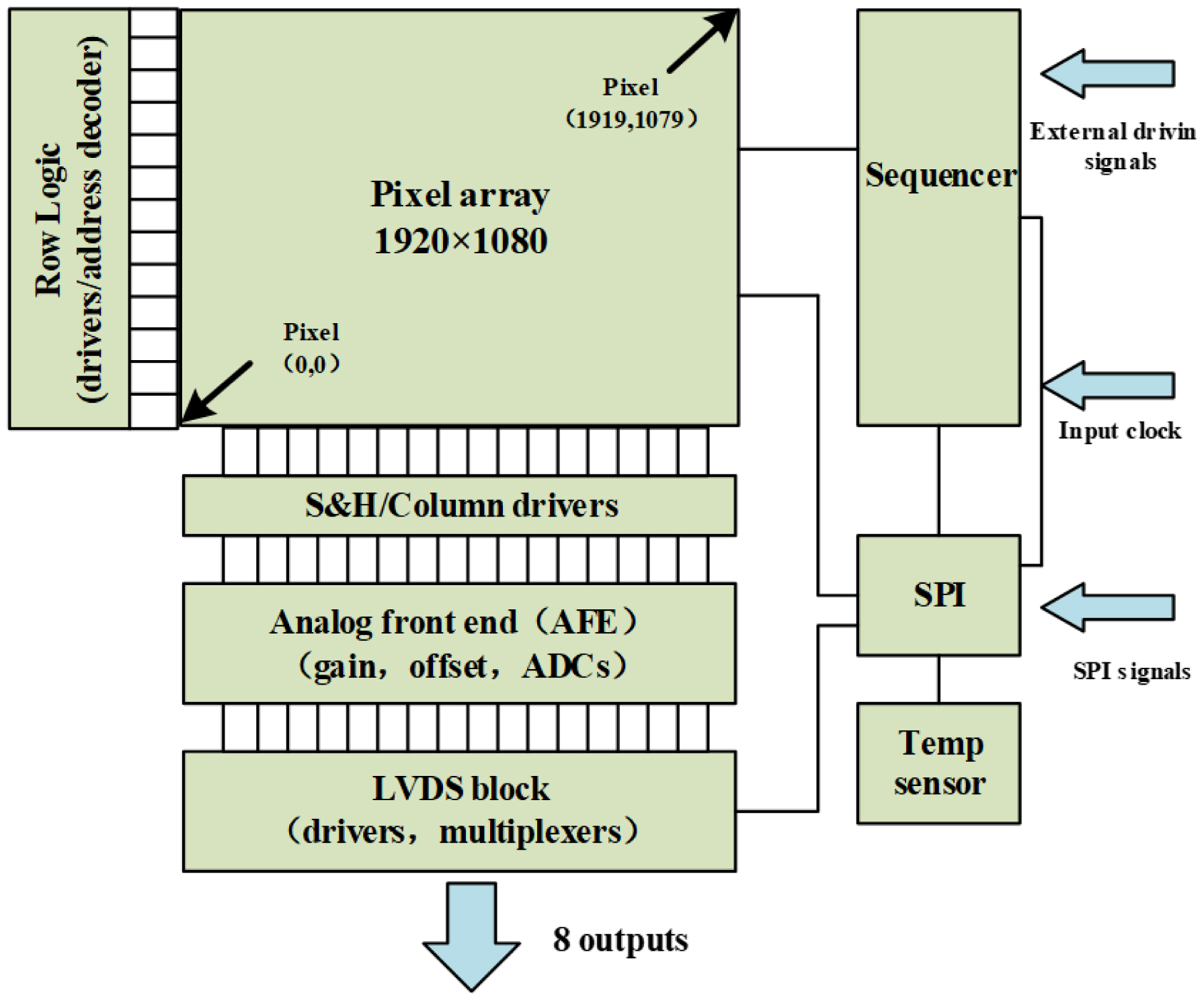
The CIS architecture.
The EMP effect was simulated for this experiment using the TEM cell irradiation method. The test device primarily comprised a pulse source, TEM cell, test board, oscilloscope, and computer, as shown in Fig. 2. The TEM cell served to maintain a constant electromagnetic field environment, while the oscilloscope monitored the electric field in the TEM cell and the voltage variation at different pins of the irradiation board. The pulse source waveforms and the Vdd port of the CIS were monitored during the test. Fig. 3 depicts the typical waveforms observed in the test. The computer test program was responsible for setting the integration time and operating state of the CIS before the test. Notably, the CIS was situated in the dark field environment during the trial, and was in the continuous map-picking operating condition during the irradiation process.
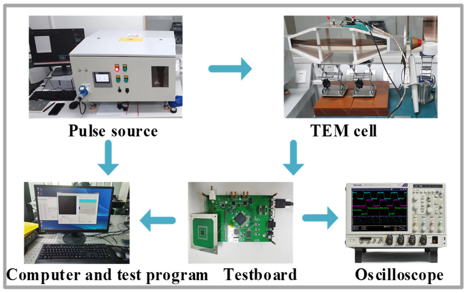
Experimental setup.

(a) Coupling voltage of Vdd and (b) pulse source of a typical waveform.
The distance between the pole plates of the selected TEM cell was 8 cm. After an oscilloscope determined the pulse voltage value inside the TEM cell, the peak field strength was determined using Eq. (1), as follows:
The main parameters of the waveform of the pulse source employed in the test were the peak field strength, rising edge time, and pulse width, as presented in Table 1. Notably, during the experiment, the rising edge time and pulse width remained unaltered—the sole variable that was adjusted was the peak field strength.

Relevant parameters of the pulse excitation source
First, a pre-experiment was conducted to estimate the CIS's failure types and their corresponding failure ranges. Based on these results, repeated irradiation tests were performed under different field strength intervals to determine the failure types and the corresponding failure criteria of the CIS as well as to obtain the interference threshold for its functional interruption.
For the pre-experiment, seven field strength intervals were set up—12.5–25.0, 25.0–37.5, 37.5–50.0, 50.0–62.5, 62.5–75.0, 75.0–87.5, and 87.5–110.0 kV/m. The results showed that the peak field strength of the pulse signal began at 12.5 kV/m and continued to increase. At least 11 irradiation tests were conducted in each field strength interval. Subsequently, the failures of the CIS that occurred during the test, along with the corresponding field strength values, were recorded. After the pre-experiment, the failure probability pertaining to each field strength interval was calculated. Notably, to avoid the influence of thermal accumulation, the CIS was powered off for a certain time interval and restarted before each test.
Finally, the interval was set to 2.5 kV/m, the number of repetitions were increased, the probability of failure was estimated, and the interference threshold at which the CIS encountered functional disruption was determined using the small sample statistical method.
III. Results
1. Failure Type
All the failure types observed in the TEM cell irradiation experiment were related to interference effects, such as image abnormality and function interruptions. Notably, more severe failure types, such as latch-up and burnout, did not occur. The details of these findings are described below.
1.1 Image abnormality
Row anomaly
At a field strength of 12.5–25.0 kV/m in the TEM cell, row anomaly, which reoccurred several times, was observed. It manifested as an abnormal gray value output of 255 DN (the maximum gray value of the CIS) for one odd row. Notably, the CIS utilized in this experiment was situated in a dark field environment, and the average gray value of the typical image was 10 DN, as shown in Fig. 4(a). Under the influence of the EMP, an abnormal gray value appeared in one line of the image, as shown in Fig. 4(b)–4(c). The phenomenon lasted for a short time and disappeared quickly, during which the CIS continued its normal operation, and the output current was maintained near the average current value.

Row anomalies: (a) normal image, (b) row anomaly, and (c) three-dimensional distribution of gray values in the row anomaly region.
Based on the characteristics of the abnormal line output, this phenomenon was attributed to the influence of coupled electromagnetic energy on the CIS's line selection register, resulting in abnormal output for the entire row. Meanwhile, this phenomenon usually occurs at a lower field strength, as the coupled electromagnetic energy is minimal at this time. Consequently, when the pulse signal disappears, the coupled energy will be rapidly depleted, leading to the restoration of the image to its normal state.
Global gray value anomaly
When the field strength within the TEM cell was 31.25–37.5 kV/m, the global gray value anomaly was observed. Similar to the row anomaly, this anomaly recurred several times. It mainly manifested as an overall increase in the average gray value of the image, which was about 106 DN—substantially higher than the 10 DN in the normal state—leading to the appearance of a dark gray image, as shown in Fig. 5(a). For further investigation, a column of the pixels in this figure was utilized to draw a gray value distribution curve. As shown in Fig. 5(b), the gray value distribution in the abnormal image is poorly uniform, indicating an increase in the internal noise of the device. Notably, the CIS worked normally and could also realize its map-picking function when this phenomenon occurred. However, unlike the line anomaly, the global gray value anomaly persisted and could only be recovered after one power cycle (power off and restart).
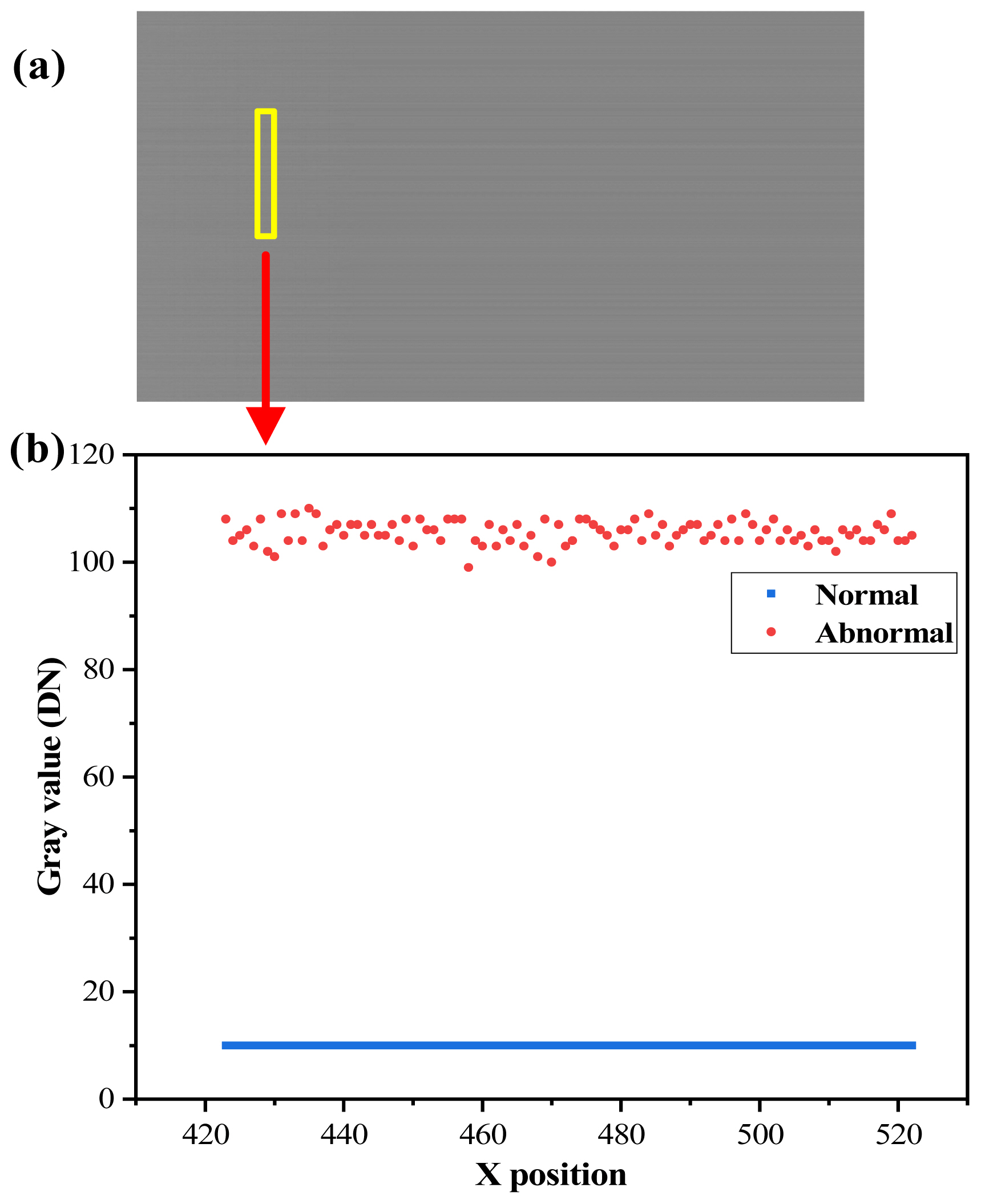
Global gray value anomalies: (a) anomalous images and (b) comparison of gray value distribution of single column pixels.
Considering that the gray value output of the abnormal image was not a constant value but showed an overall increase, this phenomenon may be considered the result of an abnormality in the offset register. In a CIS, the offset register is responsible for calibrating the output to compensate for the output signal's dark level. In this experiment, the initial offset setting value increased due to the influence of the EMP, causing the overall gray value to rise.
As shown in Fig. 5(b), pixel non-uniformity in the image exhibited a significant increase. Pulsed voltages were coupled to transfer electromagnetic signals into the device through the input and output ports, apertures, and slits. However, the generation of pulsed currents inside the device caused an increase in the noise inside it, leading to a rise in the non-uniformity of the pixel signals.
Screen distortion
The left side of the image presented in Fig. 6 shows interwoven black and white stripes that create a chaotic image. Notably, the gray pixel units on the left side of the depicted anomalous image contained gray values of 171–240 DN, while the black pixel units on the right side had 0 gray values.

Screen distortion: (a) abnormal image and (b) enlarged view of the area.
Furthermore, there are apparent differences between the abnormal phenomena on the left and right sides of the image in Fig. 6, which indicates that there may have been more than one failure site in the CIS device at the moment of EMP excitation. This could mean that multiple sites in the CIS failed simultaneously. The right side of the image displayed a gray value of 0, possibly due to the row decoder transmission gate or reset resistors being in a normally open or closed state, resulting in an output of 0 after correlated double sampling is performed. Meanwhile, the screen distortion observed on the left side of the image was likely caused by the misalignment of the LVDS output clock signal with the device operating clock signal, resulting in a scrambled output.
Analysis
The first observation drawn from the above experiments is that each image anomaly was accompanied by a corresponding failure interval. For instance, the line anomaly corresponded to 12.5–25.0 kV/m and the global gray value anomaly corresponded to 31.25–37.5 kV/m. The reason for this correspondence is that when an EMP irradiates a device, the electromagnetic signal couples the electromagnetic energy at each pin and aperture of the device through various coupling paths, which in turn affects the performance antad functions of the device. Due to the different circuit compositions and parameters of each pin in the device, the results showed variations in the coupling amount and electromagnetic resistance, i.e., different failure thresholds, for different circuit modules. As a result, different failure types occur at different failure intervals.
The second question addressed in this study is whether multiple failure conditions coincide when the field strength is substantially large. Based on the screen distortion phenomenon observed in the study findings, this coincidence seems likely. Furthermore, a failure override phenomenon has also been frequently observed, when multiple abnormal phenomena occur simultaneously, the interference phenomenon with more severe damage will take priority.
1.2 Functional interruption
Function interruption refers to the interruption in the proper functioning of the CIS in capturing images. In this study, the basis for judging functional interruption was, first, more than a 10% drop in output current and, second, interruption in the CIS continuous image acquisition function, whereby the image cannot be acquired and the normal image acquisition function can be restored only after a power cycle. When both conditions were met, the device was considered to be in a functionally interrupted state.
Fig. 7 shows that, with the output current being 300 mA during regular operation, when the CIS is subjected to an EMP, the output current exhibits a damped oscillation waveform, within 30 μs of which the current decreases to 230 mA. Moreover, various output current values were observed during the functional interruption phenomenon in the test, mainly 230 mA, 250 mA, and 280 mA, indicating that more than one mode may have caused interruptions in the device.

Output current change curve under the occurrence of functional interruption.
2. Failure Probability
Since the coupling path's randomness and excitation source instability led to a failure probability for the CIS at different field strengths, the use of the traditional small sample method to assess the interference threshold exhibited poor reliability. Therefore, this study improved upon the traditional small sample method by increasing the number of tests within the permitted range. The failure criterion involved determining the number of device failures and statistically calculate the failure probability of the device under different field strength intervals. The results of this exercise are depicted in the variation curve of the failure probability of the device with the field strength intervals in Table 2.

Failure probability for different field strength intervals
Multiple field strength intervals were considered for this test. Furthermore, repeatability tests were carried out for each field strength interval—from small to large—with the number of repetitions being greater than 11. The number of failures under each field strength interval was recorded based on the failure criterion to calculate the failure probability, as shown in Table 2. Finally, the field strength interval with a failure probability of more than 90% was identified, and the approximate interference threshold was determined. As shown in Fig. 8, when the field strength is 37.5–50.0 kV/m, the failure probability is close to 90%. Therefore, based on the results of the failure probability, the interference threshold for CIS function interruption should be within this field strength interval.
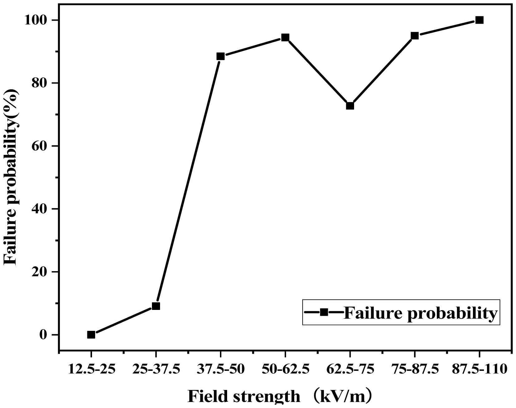
Failure probability curves for different voltage intervals.
3. Interference Threshold
Based on the results of the probability of failure, the interference threshold was determined to be roughly within 37.5–50.0 kV/m. In view of this, the field strength interval was reduced and set to 2.5 kV/m. At the same time, repeatability tests were conducted, and the number of experiments was increased. Subsequently, all the test data were arranged in sequence, from the smallest to the largest, and the related statistics were redivided according to the intervals, as shown in Table 3. Notably, the midpoint of each interval was considered the field strength value of the concerned interval. Furthermore, the peak field strength versus the failure probability curve was plotted and fitted using the three-parameter Weibull distribution function [19, 20], as shown in Fig. 9.

Failure probability for different field strength intervals
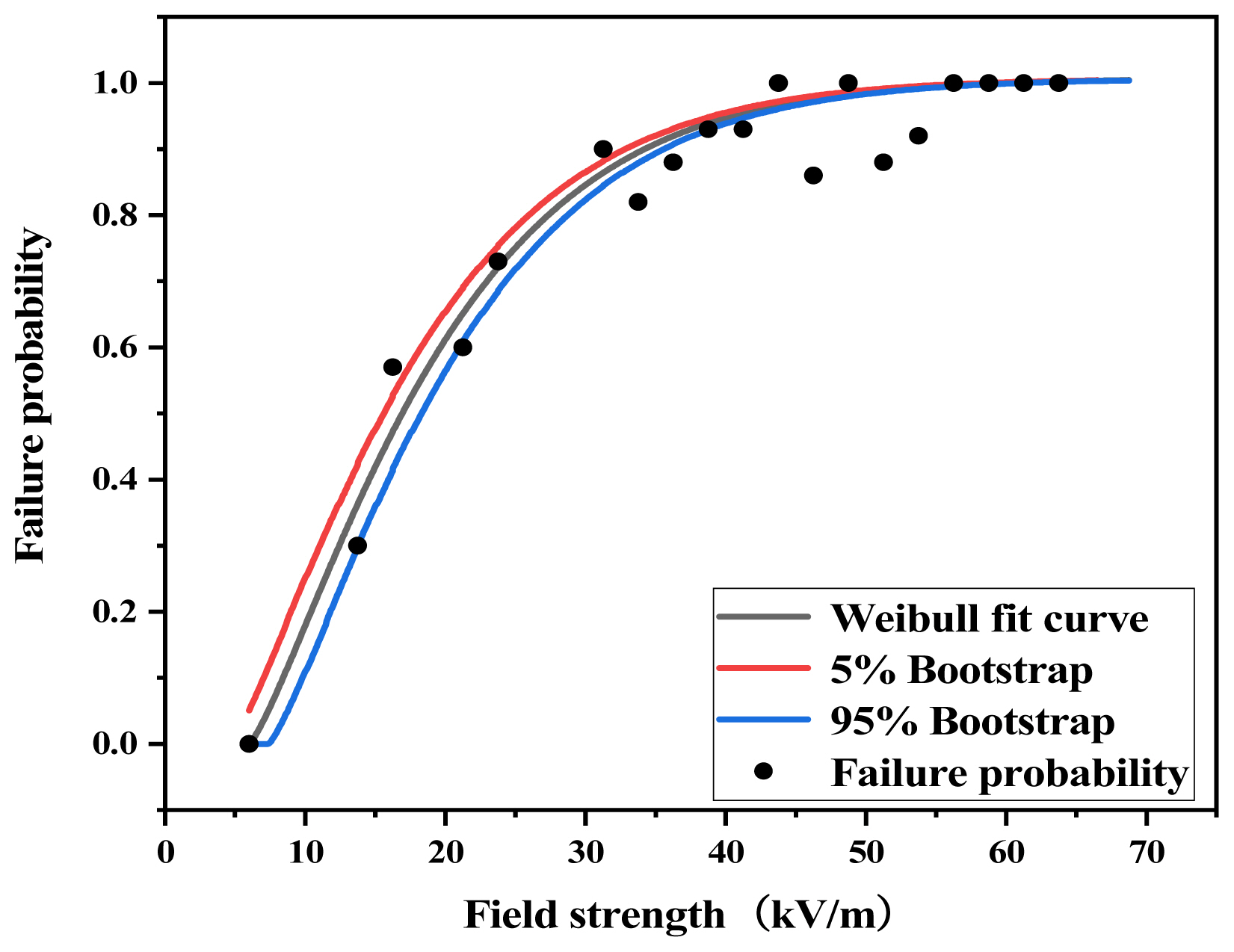
Weibull fitting curve and bootstrap interval of field strength versus failure probability.
The mathematical expression for a three-parameter Weibull distribution is
where β is the shape parameter β > 0, θ refers to the scale parameter θ > 0, and γ indicates the position parameter γ > 0. In this study, the parameters of the Weibull distribution, fitted in terms of the interference threshold, were β = 1.32, θ = 27.6, γ = 6, and R2 = 0.99487.
Furthermore, the results obtained by applying the bootstrap method [21], which was implemented to test the goodness-of-fit of the data, showed that more than 90% of the damage threshold test data fell in the 95% confidence interval of the Weibull distribution in the 0–45 kV/m interval, and thus could be applied to describe the overall distribution of the data. Furthermore, according to the results depicted by the fitted Weibull curve, when the probability of failure was 95%, the corresponding peak field strength was 40.4 kV/m. This field strength value indicates the interference threshold for CIS function interruption.
As shown in Fig. 9, several points with a low failure probability are in the field strength interval of 45–55 kV/m, mainly due to two factors. On the one hand, the randomness of the test was relatively high, indicating that subsequent testing must be increased to verify the results. On the other hand, this specific interval is located close to the field strength that caused the screen distortion. Furthermore, at this interval, the field strength is already high, and multiple modules inside the CIS are on the verge of failure. However, although the failure probability is particularly high, it does not reach the absolute failure threshold. After the peripheral circuit of the CIS is affected by a strong EMP, parasitic capacitance and inductance are generated in the equivalent circuit due to coupling effects. Effectively, owing to the mutual influence of the parasitic parameters in the circuit, the electromagnetic immunity of the CIS improves paradoxically, resulting in a slight reduction in the failure probability.
4. Interference Threshold Evaluation Method for CIS
Based on the above results, different types of CIS failures and their failure thresholds were identified. Notably, it is difficult to reasonably evaluate the interference threshold of CIS because although it bears multiple functional modules, such as the pixel unit, AD converter module, and LVDS output module, each differs from the other in terms of immunity to electromagnetic interference due to its circuit structure, ultimately exhibiting different failure thresholds. Furthermore, the immense randomness of the EMP test serves to expand the field strength range for device failure, resulting in overlapping failure intervals of multiple modules, which greatly affects failure threshold evaluation. Notably, when an anomaly occurs in the field strength range, the probability of functional disruption has been observed to be close to 70%, which significantly affects the assessment of the threshold for the appearance of the image anomaly.
Accordingly, this study took advantage of the priority relationship among different device failure types, i.e., the more severe failure type is preferred for study purposes. Since functional interruption is the most serious failure type among the many interference effects encountered by CIS, this study extracted the law of failure pertaining to functional interruption in CIS through a pre-experiment. Subsequently, the failure probability of functional interruption in the CIS was identified by utilizing the failure criterion for functional interruption, while the related interference threshold was determined using the small sample method. This relatively complete and reasonable rapid assessment method, ranging from the identification of the failure type and failure probability to the failure threshold, was developed to gauge the interference threshold of CIS.
IV. Conclusion
This paper investigates the failure types of CIS by conducting EMP simulation experiments to identify its interference effects. The identified interference effects mainly include image anomalies (row anomalies, global gray value anomalies, and screen distortion) and functional interruptions. By analyzing the characteristics of image anomalies and variations in the CIS output current, this study establishes the failure criteria for functional interruptions in CIS.
In addition, this study enhances the small sample method by increasing the number of tests within the allowable range, obtaining failure probabilities at different field strength intervals, and utilizing them at multiple field strengths to characterize the interference immunity of the device. Furthermore, the interference threshold of the device is determined and verified using Weibull distribution fitting and the bootstrap method in combination with the small sub-sample evaluation method. Notably, this paper is the first to propose a rapid assessment method—failure type to failure probability to failure threshold—to address the problems associated with assessing the immunity capability of complex systems in an HPEM environment. The research results also provide primary data and offer technical support for assessing the survivability of CIS in an HPEM environment and its related reinforcement technology.
References
Biography

Zhikang Yang, https://orcid.org/0009-0005-1754-595X received his B.S. degree from Sun Yat-Sen University, Guangzhou, China, in 2018. He is currently pursuing a Ph.D. at the Xinjiang Technical Institute of Physics and Chemistry of the Chinese Academy of Sciences, China. His current research interests include radiation effects and electromagnetic compatibility in electronic components, such as CMOS image sensors.

Lin Wen, https://orcid.org/0000-0003-4921-6147 received his Ph.D. degree from the Xinjiang Technical Institute of Physics and Chemistry of the Chinese Academy of Sciences, Urumqi, in 2015. His research interests include radiation effects and mechanisms, experimental evaluation methods, and radiation hardness design technology for space-borne photoelectric devices and systems.

Yudong Li, https://orcid.org/0000-0001-8496-5851 received his Ph.D. degree in 2009 from the Changchun Institute of Optics, Fine Mechanics and Physics, Chinese Academy of Sciences, China. He is currently a researcher at the Xinjiang Technical Institute of Physics and Chemistry, Chinese Academy of Sciences, China. His research interests include radiation effects and mechanisms, experimental evaluation methods, and radiation hardness design technology for space-borne photoelectric devices and systems.

Dong Zhou, https://orcid.org/0000-0001-8705-9838 received his Ph.D. degree from the Xinjiang Technical Institute of Physics and Chemistry of the Chinese Academy of Sciences, Urumqi, in 2013. His research interests include radiation effects and mechanisms of space-borne photoelectric devices and materials.

Xin Wang, https://orcid.org/0009-0003-6498-2197 received her Ph.D. degree from the School of Microelectronics and Solid Electronics, Xinjiang Technical Institute of Physics and Chemistry of the Chinese Academy of Sciences, Urumqi, in 2016. Her current research interests include characterizing radiation-induced defects in electronic components and materials.

Rui Ding, https://orcid.org/0000-0003-2854-6315 received his M.S. degree from Anhui University of Technology in 2023. He is currently a researcher at the China Electronic Product Reliability and Environmental Testing Research Institute, Guangzhou, China. His current research interests include electromagnetic compatibility and high-power pulse technology.

Meuqing Zhong, https://orcid.org/0009-0004-0210-8207 received her B.S. degree from Tsinghua University, Beijing, China, in 2020. She is currently pursuing a Ph.D. in nuclear science and technology at Tsinghua University. Her current research interests include radiation effects and electromagnetic compatibility in electronic components, such as bipolar transistors.

Cui Meng, https://orcid.org/0000-0002-0416-4315 is currently a professor at the School of Electrical Engineering in Zhejiang University. Her research interests include assessing high-power electromagnetic environmental effects and the scientific problems associated with transient ionizing radiation-excited intense electromagnetic pulses.

Wenxiao Fang, https://orcid.org/0000-0002-9839-0777 received his Ph.D. degree from Sun Yat-sen University, Guangzhou, China, in 2008. His research interests include electromagnetic environmental effects, integrated circuits, and microsystem electromagnetic compatibility evaluation and modeling.

Qi Guo, https://orcid.org/0000-0003-4188-6883 is the Director of the Solid State Radiation Physics Research Laboratory at Xinjiang Institute of Physics and Chemistry, Chinese Academy of Sciences. He is mainly engaged in researching ionizing radiation effects, damage mechanisms, and experimental evaluation methods for electronic components.