Design of 39-GHz Up- and Down-Conversion Mixers for 5G mmWave TDD Applications
Article information
Abstract
This article presents fully integrated 39-GHz bidirectional up- and down-conversion mixers for 5G millimeter-wave (mmWave) applications. Fabricated in a 65-nm CMOS process with a 1.2-V supply voltage, the up- and down-conversion mixers consume 39 and 43 mW, respectively. For 5G time-division duplexing (TDD) operation, intermediate-frequency (IF)/local-oscillator (LO)/radio-frequency (RF) T/R switches are introduced. For better isolation and low insertion loss between the up- and down-conversion mixer, a series-shunt single-pole double-throw (SPDT) structure and an equivalent lumped λ/4 transmission line are proposed for IF and RF T/R switches, respectively. To realize compact area and wide bandwidth, a transformer-based matching network is adopted in this design. Targeting multi-channel phased array applications, the measurement result shows that the up-conversion mixer achieves a 2.5-dB peak conversion gain with 6.5 GHz 3-dB bandwidth. Including the insertion loss of the switch and IF signal routing, at the maximum gain of 36.5 GHz, the up-conversion mixer achieves an output 1-dB gain compression point (OP1dB) of 2.5 dBm. Furthermore, the down-conversion mixer achieves a 5-dB peak conversion gain with a 9.7-GHz 3-dB bandwidth.
I. Introduction
Due to high data rates and low latency, the fifth-generation (5G) commercial wireless communication system has developed rapidly. According to 3GPP, millimeter-wave frequency bands, such as 28- and 39-GHz, are used for 5G new radio (NR). Recently, several 28- and 39-GHz transceiver systems for 5G communication have been reported [1–4]. As crucial building blocks in the transceiver system, up- and down-conversion mixers have been widely studied. Several up-conversion mixers have been realized [5–8]. To improve conversion gain and bandwidth performance, cross-coupled neutralization capacitors were introduced in LO inputs ports [5]. To enhance the third-order output intercept point (OIP3), a cross-coupled pair working in the weak inversion region was introduced [6]. A complementary derivative superposition technique with pre-distortion was introduced for high linearity with the penalty of relative implementation complexity [7]. The 27.5–43.5 GHz up-conversion mixers with high linearity are proposed for 5G communication by using the linearized transconductance stage [8]. On the other hand, several down-conversion mixers have been proposed [9, 10]. A 28 GHz, single-balanced down-conversion mixer with active loads was realized to improve the gain performance [9], and a Ka-band down-conversion mixer was proposed [10]. For high conversion gain and wide bandwidth, dynamic current injection and resonating peak control techniques were used, although their power consumption was relatively high. Note that works cited above mainly focused on individual millimeter-wave (mmWave) up- and down-conversion mixers; for 5G phased array communication applications, it is important to realize fully integrated bidirectional time-division duplexing (TDD) up- and down-conversion mixers with compact areas. Moreover, considering the driving issues of the multi-channel phased array front-end circuits, bidirectional up- and down-conversion mixers should have exceptional linearity performance.
To address the above issues, in this paper, compact fully integrated bidirectional up- and down-conversion mixers were proposed for 5G mmWave TDD operation. To improve the mixer performance for phased array applications, several circuit improvements were offered. First, for compact area and wide bandwidth performance, the transformer-based matching network was used. Second, to realize TDD operation and low switching loss, the series-shunt structure and the equivalent lumped λ/4 transmission line were proposed for intermediate-frequency (IF) and radio-frequency (RF) T/R switches, respectively. Third, for high linearity and gain performance, the common source (CS) RF and IF buffers were adopted with capacitive cross-coupling neutralization techniques. For performance demonstration, the fully integrated 39-GHz bidirectional up- and down-conversion mixers were realized with a 65-nm CMOS process with a chip area of 0.42 and 0.48 mm2, respectively. With these measurements, the proposed bidirectional up- and down-conversion mixers achieved a peak conversion gain of 2.5 and 5 dB, respectively.
This paper is organized as follows. Section II presents the system analysis and design of the up- and down-conversion mixers. Section III presents the measurement results. Section IV presents the conclusion.
II. System Analysis and Design
1. Antenna Shape
The proposed bidirectional up- and down-conversion mixers are shown in Fig. 1, which consist of IF/RF T/R switches, TX path, RX path, and LO path. The TX path includes an upconversion mixer and RF buffer, and the RX path includes a down-conversion mixer and IF buffer. Two LO buffers and an LO T/R switch are included in the LO path.
2. TX Path
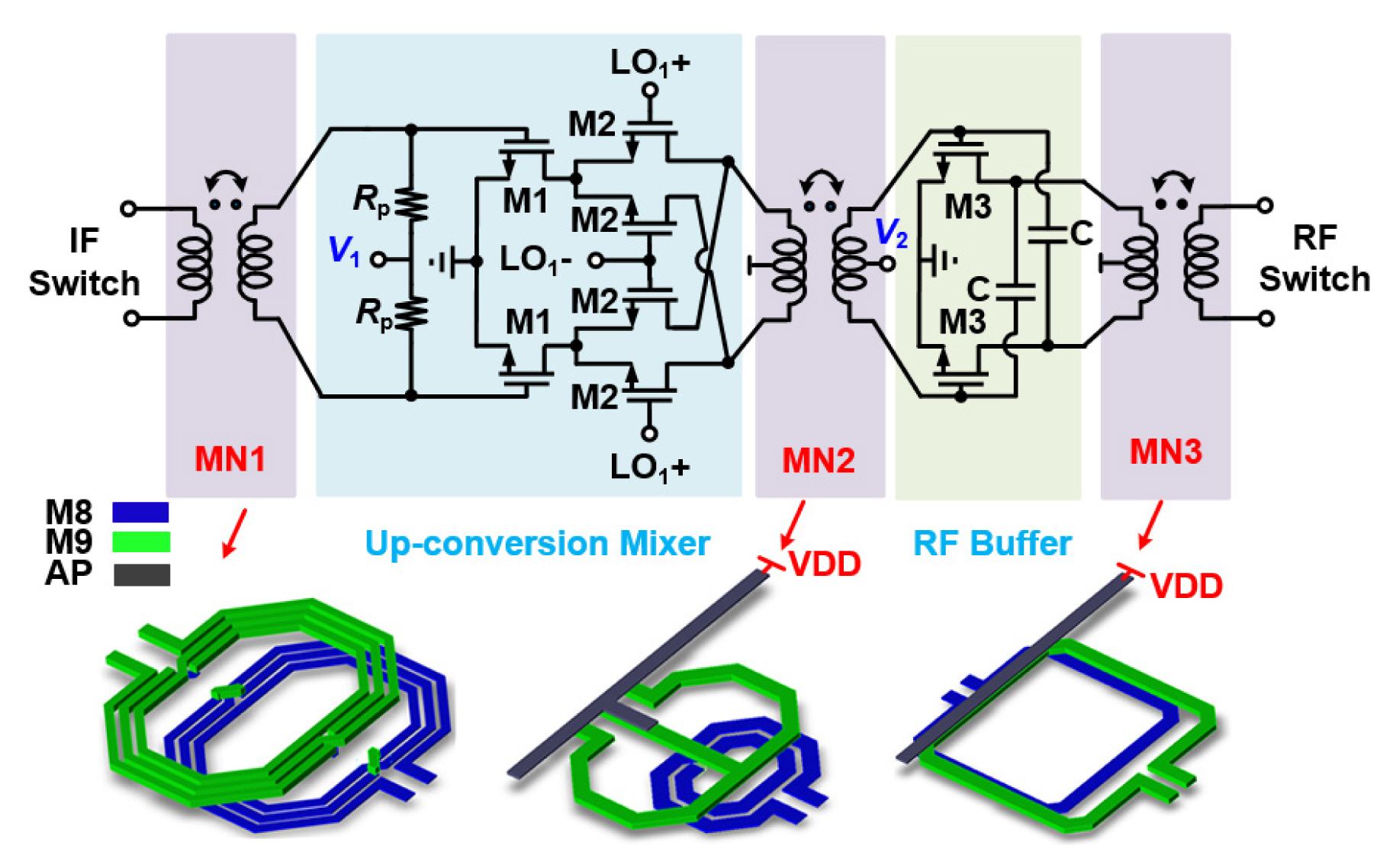
Fig. 2 shows the schematic of the TX path. The active mixer and passive mixer are most commonly used structures for the up-conversion mixer. Unlike the passive mixer, the active mixer can typically achieve relatively high conversion gain and linearity performance with a low LO power. In this work, to achieve a high conversion gain and better linearity, the active Gilbert structure was adopted. Moreover, for wide bandwidth and DC isolation between two blocks, the transformer-based matching network was used to realize two resonance frequencies with a proper mutual coupling factor k [13, 14]. The layout of transformer-based matching networks is shown in Fig. 2. As indicated, the voltage supply was fed at the center tap of the transformer, simplifying the implementation complexity. To enhance the inductor Q performance, the top thick metals were used for the transformer primary and secondary windings, respectively.
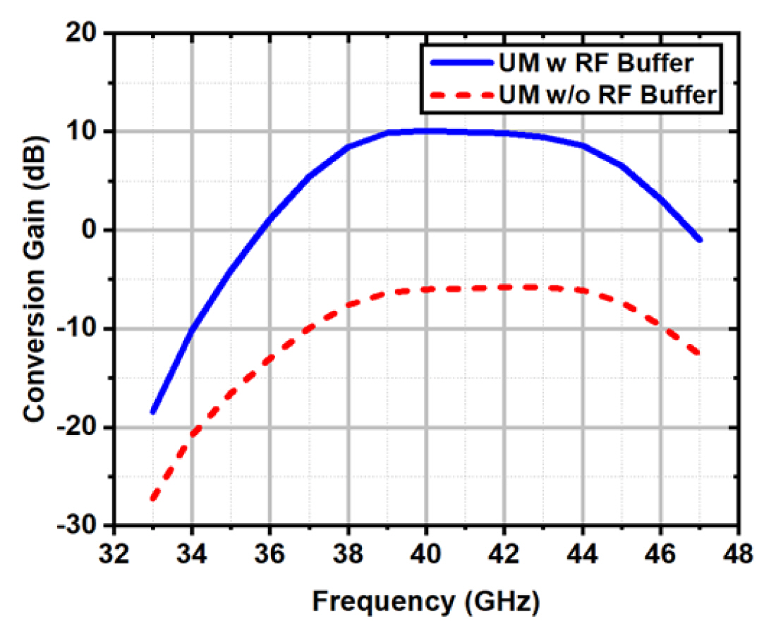
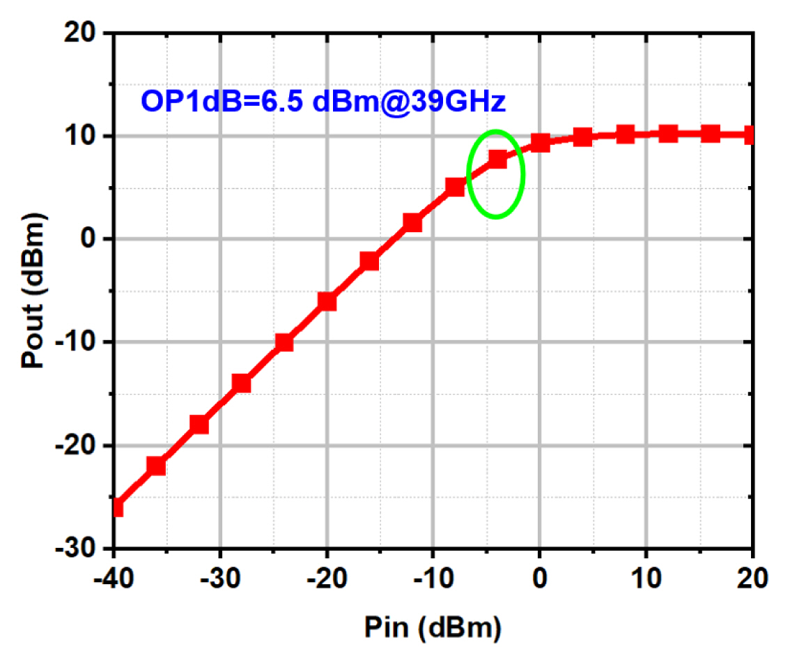
Considering the power amplifier driving purpose, a CS RF buffer was introduced to achieve better linearity and high conversion gain. Normally, due to the capacitive parasitics in the mmWave frequency, the CS RF buffer has stability and gain reduction issues. To address these concerns, the capacitive cross-coupling neutralization technique was used simultaneously enhancing the amplifier gain and stability. To illustrate the effect of the RF buffer, the simulation results of the up-conversion mixer with and without the RF buffer are shown in Fig. 3. With 1.5 dBm 33 GHz LO, the up-conversion mixer achieves 10 dB and −5.3 dB peak conversion gains with and without RF buffer, respectively. Fig. 4 shows the simulated RF output power of the up-conversion mixer versus the IF input power. As indicated, with a CS RF buffer, the output 1-dB gain compression point (OP1dB) can reach 6.5 dBm at 39 GHz.
3. RX Path
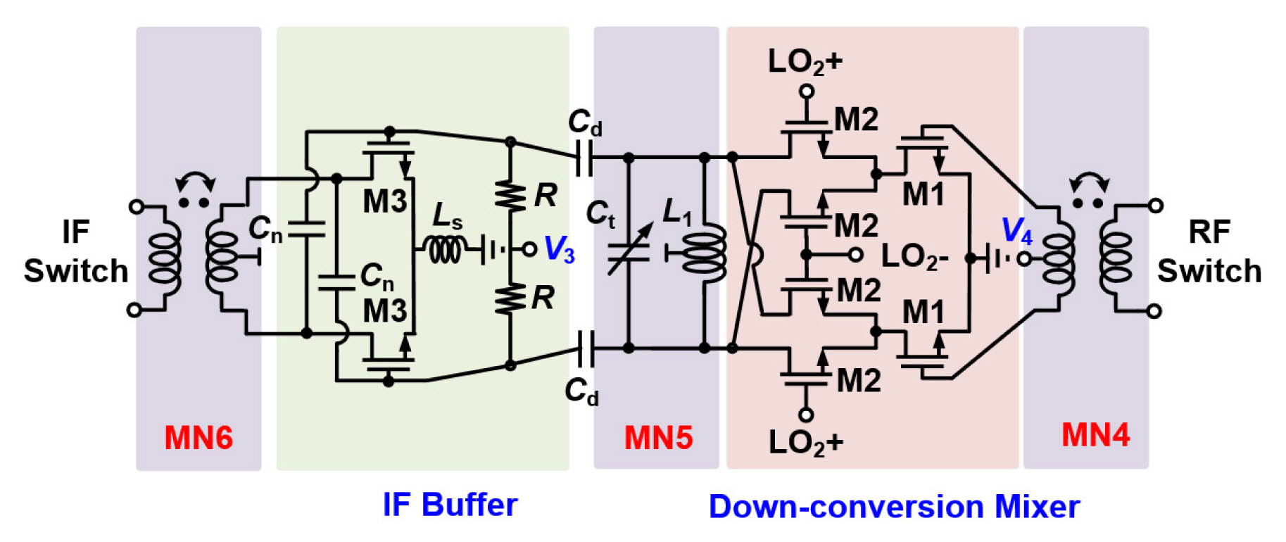
Fig. 5 shows the schematic of the RX path. To achieve a high conversion gain and low noise figure (NF), the active Gilbert mixer structure was also adopted for the down-conversion mixer. Port isolation can be promoted with a careful layout of the double-balanced down-conversion mixer. To achieve wide bandwidth, the switch capacitor array Ct was introduced. To drive the IF transceiver, a differential CS IF buffer was used. Note that, under these simulations, the high Q input impedance of the IF buffer will deteriorate its bandwidth performance. To solve the problem, a parallel resistor R and source degeneration L were introduced, offering greater design freedom in bandwidth optimization. Considering the trade-off between gain and bandwidth, the resistor R and the inductor L are optimized to be 800 Ω and 300 pH, respectively.
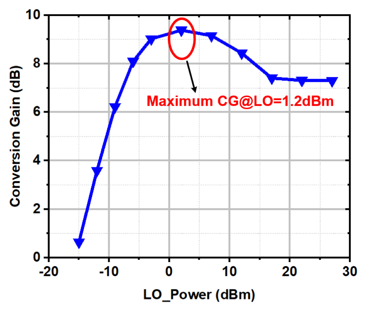
Fig. 6 shows the simulated conversion gain of the down-conversion mixer versus the LO power. As presented, the down-conversion mixer achieves a maximum conversion gain of 9 dB with 1.2 dBm LO power.
4. LO Path
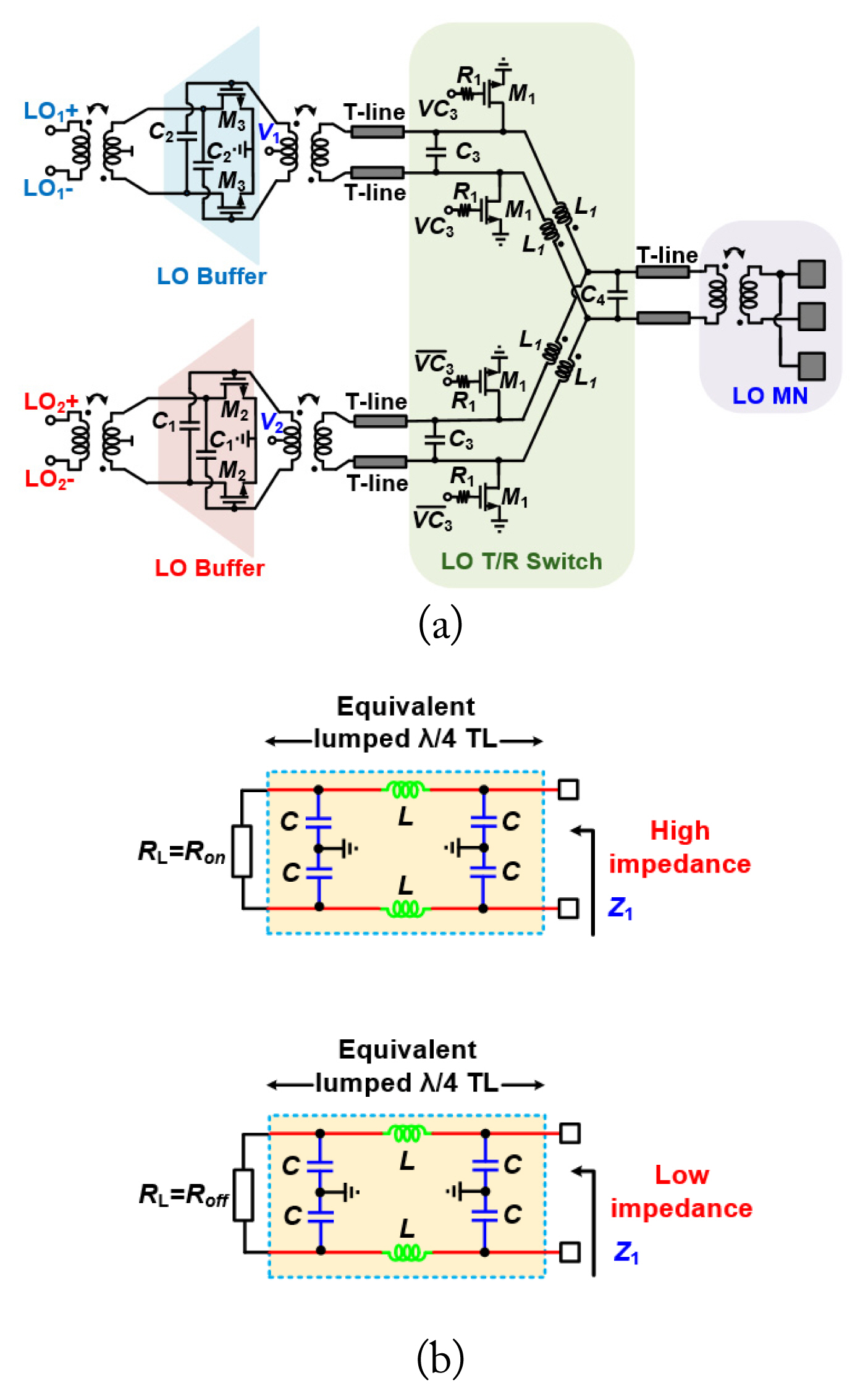
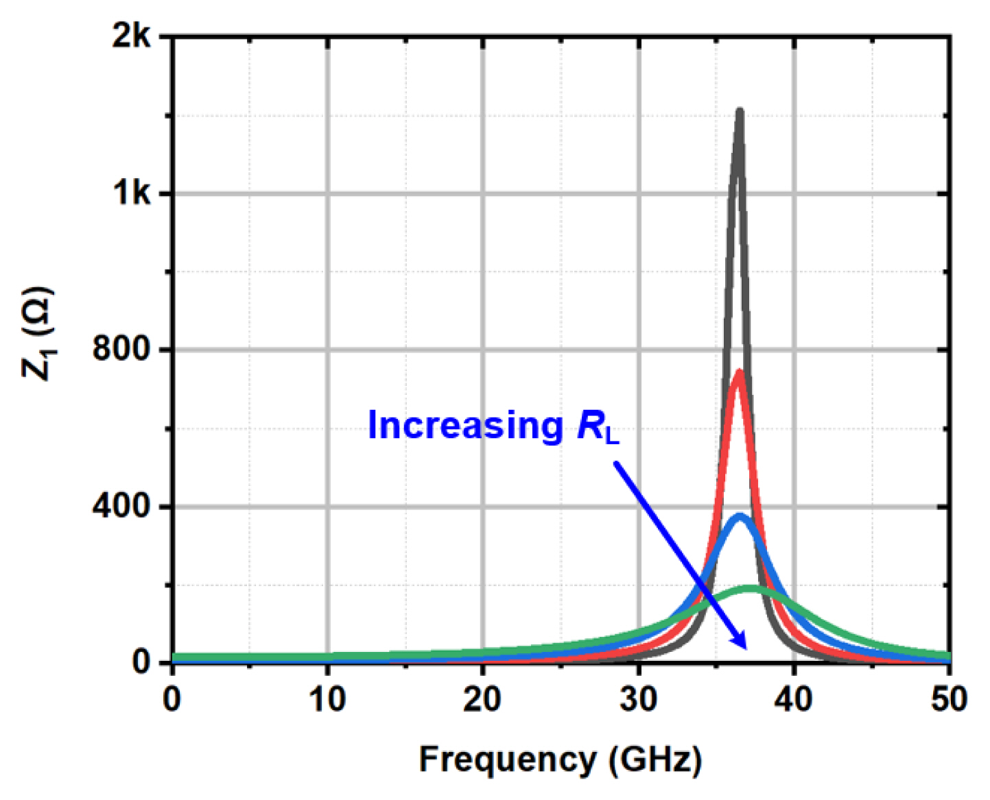
To provide sufficient LO power for the up- and down-conversion mixers, two LO buffers are included in the LO path, as shown in Fig. 7(a). As indicated, the LO T/R switch was proposed to realize the TDD operation. Traditionally, series, and series-shunt SPDT (single-pole double-throw) are the most commonly used T/R switch structures [15–17]. However, due to the very high operating frequency, the insertion loss and isolation performance of the SPDT switch at mmWave frequency are worsened by the transistor parasitics. To reduce the parasitic capacitance influence at mmWave frequency, the equivalent lumped λ/4 transmission line was introduced, as shown in Fig. 7(a)[17, 18]. To illustrate the working principle of the LO T/R switch, Fig. 7(b) shows the simplified C-L-C impedance network. Note that, Ron and Roff are the on and off resistances of transistor M1, respectively. When M1 is on, Ron is small, realizing high impedance Z1 due to the impedance transformation. In contrast, when M1 is off, and Roff is large, Z1 has low impedance. The dependence of the output impedance Z1 of the equivalent lumped λ/4 transmission line on the different load impedance RL is shown in Fig. 8. As indicated, the output impedance Z1 is reduced when RL increases, and vice versa. In other words, it can be concluded that the smaller the resistance of M1, the smaller the insertion loss of the switch, thereby approaching the ideal switch. However, by enlarging the transistor size, the parasitic capacitance increases, reducing the switch isolation. In this design, based on the simulation results, the width of M1 is optimized by balancing between switch isolation and insertion loss performance.
5. IF/RF T/R Switches
For 5G TDD operation, IF/RF T/R switches are key building blocks. In this design, as the IF working frequency is around 6–7 GHz, compared with RF and LO frequencies, it was less affected by parasitic capacitance. Therefore, the series-shunt structure was used to realize the switching operation. Since the RF frequency is higher than the LO frequency, the above presented equivalent lumped λ/4 transmission line is also adopted to realize the RF T/R switch.
III. Implementation and Measurement Results
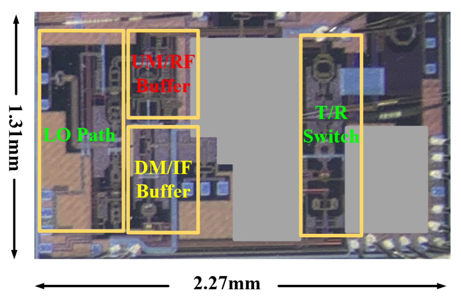
As shown in Fig. 9 and fabricated in the 65-nm CMOS process, the up- and down-conversion mixers occupy 0.42 and 0.48 mm2 chip areas, respectively. Note that, for phased array system realization, the IF signal has a 1-mm routing length. With a 1.2-V supply voltage, the up-conversion mixer consumes 39 mW, in which the LO buffer and TX path consume 11 and 28 mW, respectively. For the TX path, the up-mixer and RF buffer consume 13 and 15 mW, respectively. The down-conversion mixer consumes 43 mW, in which the LO buffer and the RX path consume 11 and 32 mW, respectively. For the RX path, the down-mixer and IF buffer consume 15 and 17 mW, respectively.
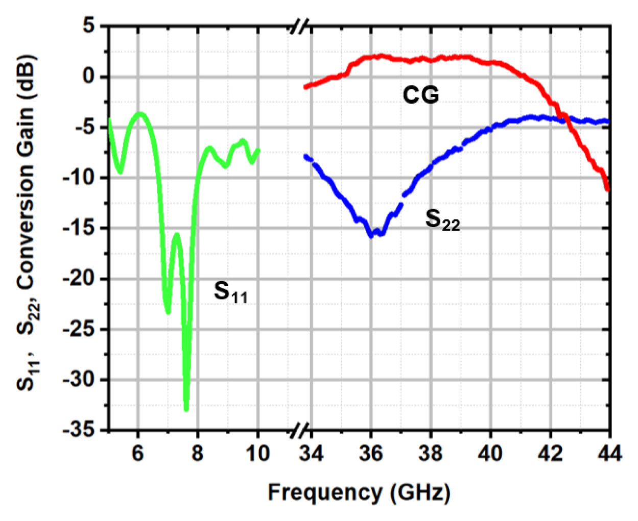
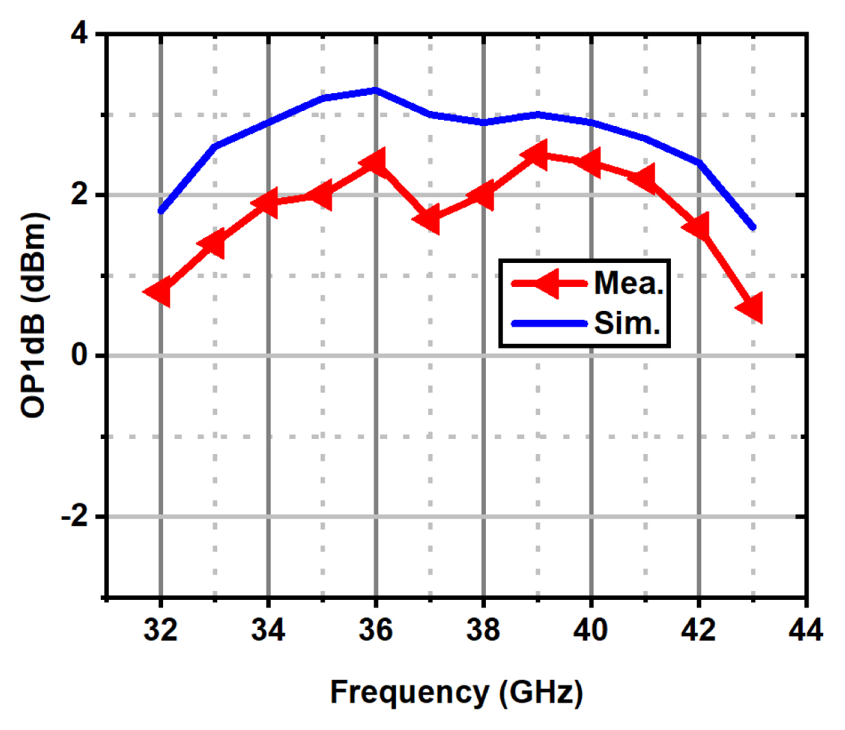
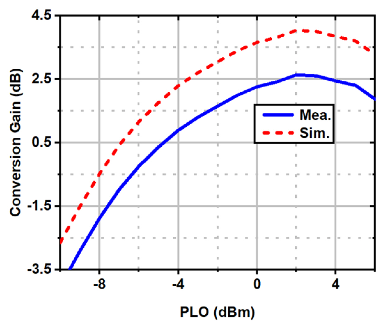
By sweeping the LO frequency from 26 GHz to 38 GHz, the S-parameters of the up-conversion mixer are measured. As shown in Fig. 10, the up-conversion mixer achieves a 6.5-GHz 3-dB bandwidth from 34.7 GHz to 41.2 GHz. Over the above frequency range, the input and output return loss are better than −10 and −5 dB, respectively. Fig. 11 compares the measured and simulated OP1dB results. As indicated, the up-conversion mixer achieved a measured OP1dB from 0.6 to 2.5 dBm, and due to the underestimated parasitics, there existed some differences between the measurement and simulation results. The measured and simulated conversion gain versus the LO power are shown in Fig. 12. According to the measurement results, 2 dBm LO power is sufficient for the up-conversion mixer to achieve the appropriate conversion gain.
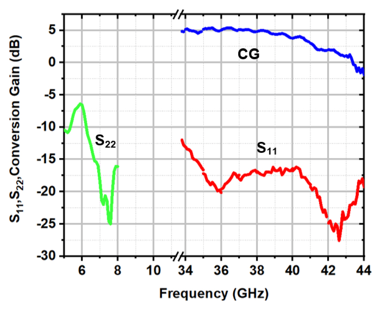
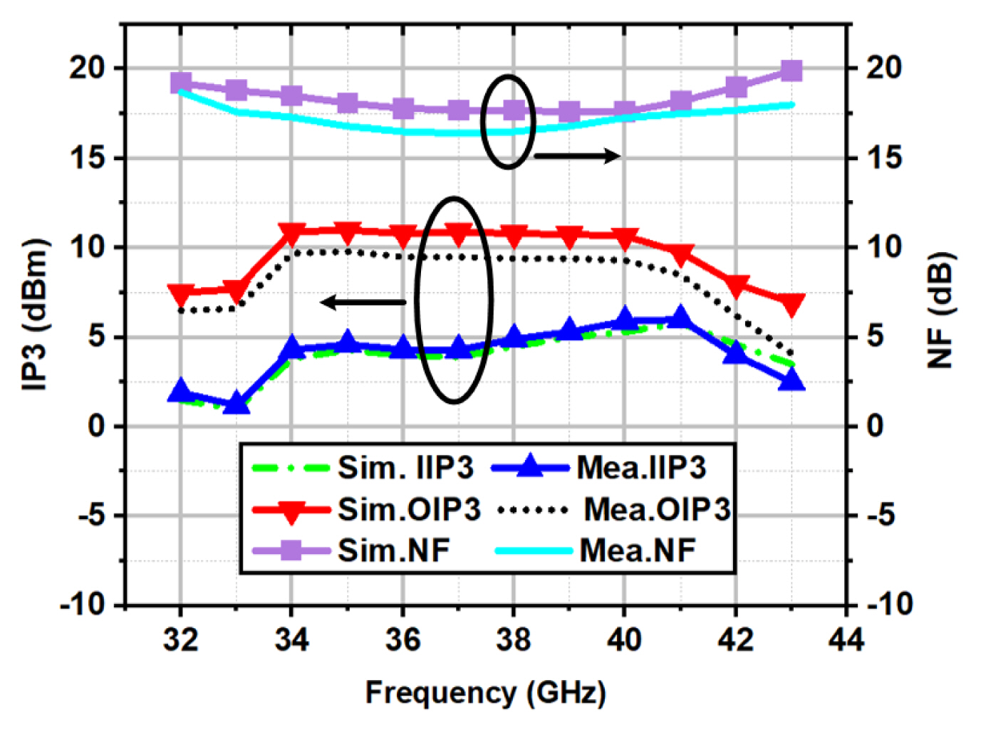
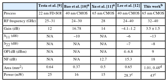
Fig. 13 shows the measured S-parameters of the down-conversion mixer. By sweeping the LO frequency from 26 GHz to 38 GHz, the down-conversion mixer achieves 8 GHz 3-dB bandwidth from 32 GHz to 40 GHz, with a peak gain of 5 dB. Moreover, the input and output return losses are better than −10 and −8 dB, respectively. Fig. 14 presents the measured and simulated NF and IIP3 (input third-order intercept point), respectively. From 32 GHz to 40 GHz, the measured NF varied from 17.5 to 18 dB, with the lowest NF of 17.5 dB at 39 GHz. Moreover, the measured OIP3 and IIP3 are in the range of 4–6 dBm and 8.4–9 dBm, respectively. Note that the difference in the measured and simulated results may be caused by underestimated parasitic parameters. For performance comparison, Table 1 summarizes the performance of the up-conversion mixer and compares it with the state-of-the-art up-conversion mixer results [5–8]. As indicated, the up-conversion mixer achieves competitive overall performance, in particular high linearity and gain performance with a compact chip area. Table 2 summarizes the performance of the proposed down-conversion mixer and the state-of-the-art results [9–12]. As shown in Table 2, when comparing the chip with measurement results, the down-conversion mixer achieves high linearity performance with the lowest chip area. Note that the above bidirectional 39-GHz up- and down-conversion mixer results are achieved even with the 1 mm IF routing length and TDD switch, whose losses are both about 2 dB, respectively.
IV. Conclusion
In this paper, fully integrated bidirectional up- and down-conversion mixers for 5G TDD operation are proposed. By sharing IF/RF T/R switches between up- and down-conversion mixers, routing and circuit complexity were reduced. The RF and IF buffers were adopted to enhance the gain and linearity performance of the up- and down-conversion mixers. Fabricated in a 65-nm CMOS process, the up- and down-conversion mixer areas are 0.42 and 0.48 mm2, respectively. The up-conversion mixer achieved a 6.5-GHz 3-dB bandwidth, with a peak OP1dB of 2.5 dBm, while the down-conversion mixer achieved a 8-GHz 3-dB bandwidth, with a lowest NF of 17.5 dB at 39 GHz.
Acknowledgments
This work was supported by the National Key R&D Program of China (Grant No. 2018YFE0205900) and in part by the Major Key Project of PCL (Grant No. PCL 2021A01-2).
References
Biography

Yiyang Wang received a B.S degree from the Anhui University of Finance and Economics, Bengbu, Anhui, in 2014, and a M.S. degree from Southeast University, Nanjing, China, in 2018, where he is currently pursuing the Ph.D. degree in information engineering. His current research interest includes wireless communication transmitter systems for 5G.

Haipeng Duan received a B.S. degree in communication engineering from Zhengzhou University, Zhengzhou, China, in 2016. He is currently pursuing a Ph.D. degree in the National Mobile Communications Research Laboratory, Southeast University, Nanjing, China. His current research interests include RF and millimeter-wave CMOS integrated circuits for communication.

Long He received a B.S. degree in communication engineering from Zhengzhou University, Zhengzhou, in 2011. Then, he received a M.S. degree in integrated circuit design and a Ph.D. degree in circuit and system from Southeast University, Nanjing, China, in 2014 and 2019, respectively. Since 2019, he has been working at the Purple Mountain Laboratory as an IC design engineer. His present research interests focus on high-performance analog-integrated circuits for mmWave-phased array systems.

Xu Wu was born in Hebei, China, in 1983. She received a bachelor’s degree from the Huazhong University of Science and Technology in 2001, a M.S. degree in industrial engineering in electronics (industrieel ingenieur electronica) from GROEP T, Belgium, in 2005, and a Ph.D. degree in electronics from the Katholieke Universiteit Leuven (KU Leuven), Leuven, Belgium, in 2012. She has worked as a Research Assistant with the Laboratory ESAT, MICAS Group, KU Leuven. From 2011 to 2017, she worked with the CMOSIS, Belgium, as a Senior Design Engineer and a Technique Lead. Her main target was to develop advanced high-speed CMOS image sensors. Since 2017, she has been working as a Faculty Member of Southeast University, China. Her current research interests include RF transceivers, and high-performance and high-frequency analog-integrated circuits for telecommunication systems.

Dongming Wang (Member, IEEE) received a B.S. degree from the Chongqing University of Posts and Telecommunications in 1999, a M.S. degree from the Nanjing University of Posts and Telecommunications in 2002, and a Ph.D. degree from Southeast University, China, in 2006. He joined at the National Mobile Communications Research Laboratory, Southeast University, in 2006, where he is currently a professor. His research interests include signal processing for wireless communications and large-scale distributed MIMO systems (cell-free massive MIMO).

Lianming Li was born in Henan, China, in 1978. He received a B.S. degree in physics and a M.S. degree in electrical engineering from Southeast University, Nanjing, China, in 2001 and 2004, respectively. He received a Ph.D. degree from Katholieke Universiteit Leuven (KU Leuven), Leuven, Belgium, in 2011. From 2006 to 2011, he was a Research Assistant with the Laboratory ESAT, MICAS Group, KU Leuven, where he was involved in mmWave CMOS design. Since 2011, he has been an Associate Professor with the School of Information Science and Engineering, Southeast University. His current research interests include mmWave circuits and system design, antennas and packaging design, and frequency generation circuit design.

