


I. Introduction
Recently, the demand for low-power and small radar sensors for monitoring and presence detection has drawn attention to the fully integrated radar IC solution. Although there are other potential radar candidates, such as Doppler and frequency-modulated continuous wave (FMCW) radars, the impulse radio ultra-wideband (IR UWB) radar has the advantages of a high resolution, a relatively simple design, and potentially low power realization [1ŌĆō7].
Given the allocated ultra-wideband (UWB) bands because of sub-6 GHz 5G communication devices and spectrum regulation, the 3ŌĆō5 GHz band is practically not useful; instead, the higher band of 6ŌĆō10 GHz is available for UWB applications. Although this higher band has many benefits, such as the smaller form factor of the antenna and fewer interferers from nearby commercial RF signals, however, more path loss reduces the detection range and results in the worse performance of the radar circuits. As a short detection range is one of the major drawbacks of UWB radar sensors compared with their competitors, especially FMCW radars, maximum detection range extension is a critical point during the use of actual applications.
The maximum detection range for a given target or reference radar cross-section (RCS) strongly depends on the architecture and sensitivity of the receiver. The UWB signal is an impulse signal, and very high-speed sampling (more than Gsps) is required for a centimeter-high resolution.
Several papers have been published on the full UWB radar transceiver [1ŌĆō7]. The direct sampling receiver of the millimeter-level resolution is used for breathing rate motoring applications [2, 5, 6]. Another solution to mitigate the difficulties of high-speed direct sampling is to use a correlation receiver. The UWB carrier is removed, and the lower-frequency envelope signal, whose bandwidth is below 1 GHz, is sampled at the receiver end.
The self-mixing architecture of correlation receivers can be easily designed and is robust against small, undesired noise [4, 7]. However, as the gain of the self-mixing receiver is proportional to the square of the mixer input magnitude, in the case of very small RF input, which is probably reflected from the far-distant target, the receiver has a much smaller gain, and the target becomes hardly detectable. This problem, in turn, leads to a short detection range and poor receiver sensitivity. Conversely, a correlation receiver with a local oscillator (LO) or an LO correlation receiver can be used, as its conversion gain is much higher than that of the self-mixing receiver for the small-reflected signal [3]. The LO signal comes from the voltage-controlled oscillator (VCO), which is simultaneously used for transmitter impulse generation. As the same VCO is used both for the transmitter and the receiver, the receiver is coherently correlated and robust against phase noise and frequency drift.
To achieve a cm-level resolution, the equivalent time sampling (ETS) technique, which is a type of undersampling, is commonly applied [1]. With the ETS technique, a high-speed sampling of 2 Gsps is obtained equivalently at the cost of a longer scan time. The pulse repetition interval and sampling time spacing are 100 ns and 0.5 ns, respectively, which correspond to the 15 m detection range and 7.5 cm resolution. The 6-bit flash-type analog-to-digital converter (ADC) with 1 GHz input bandwidth is integrated together.
The UWB transmitter uses the switched VCO topology. It is composed of a VCO shared with the receiver, a pulse generator, and a pulse shaper. These generate short periodic control pulses using the reference clock coming from the delay looked loop (DLL). The receiver architecture is the correlation receiver using the LO signal from the VCO. By mixing with the LO source, the improved receiver gain and the phase information are achieved. The UWB radar IC is implemented in a 0.13 ╬╝m CMOS process and measured. The rest of this paper is organized as follows. In Section II, the architecture design is presented. Section III provides the circuit design of the transceiver. In Section IV, the measurement results are discussed, and in Section V, the summary and conclusion are given.
II. UWB Radar Architecture
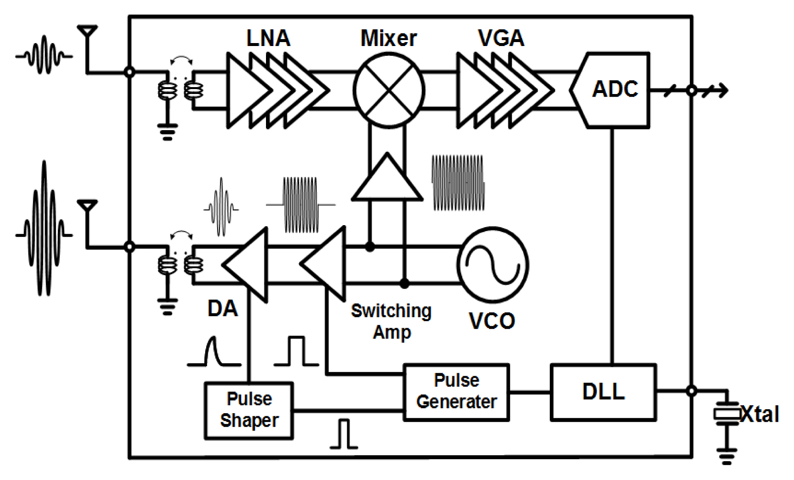
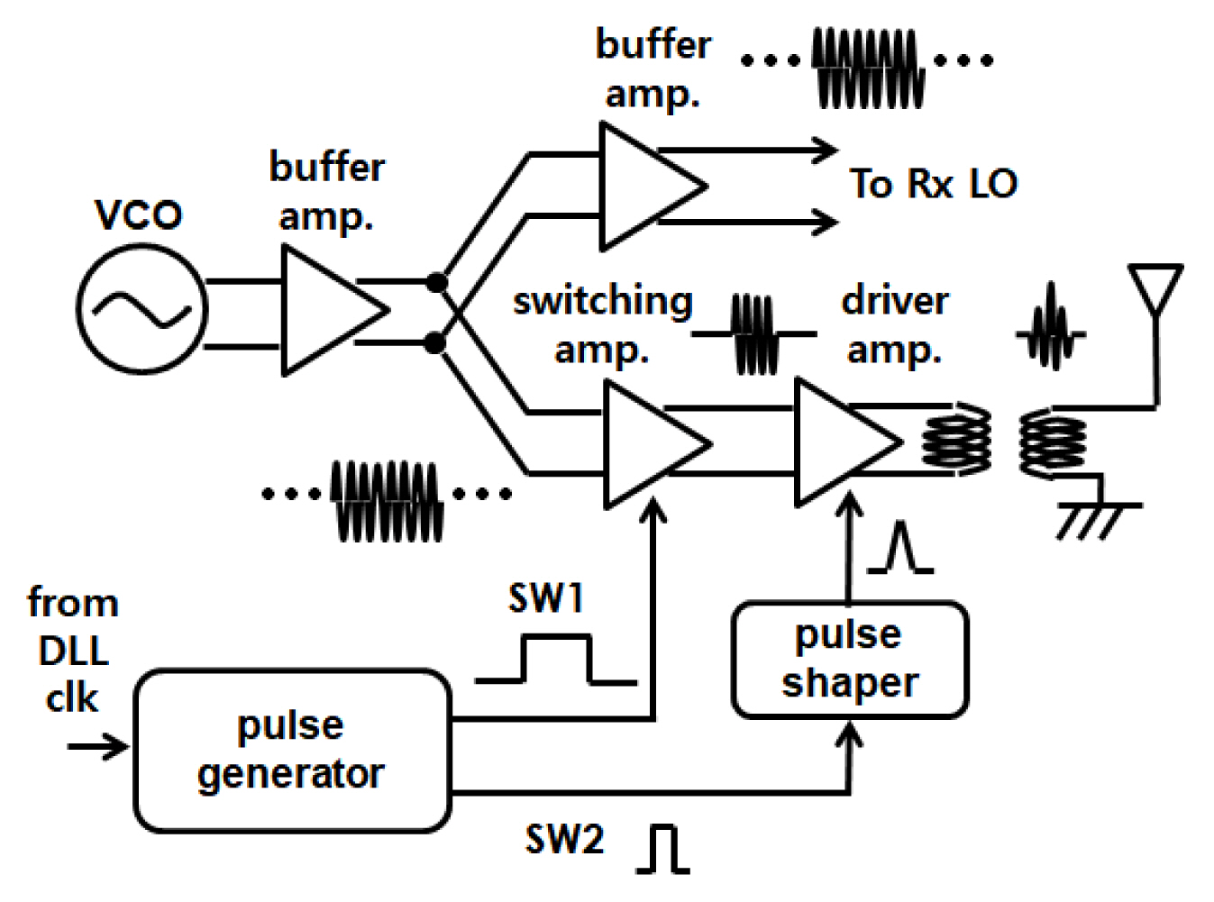
Fig. 1 shows the block diagram of the UWB radar IC proposed in this paper. The transmitter is a carrier-based impulse generator that uses the VCO and switching circuits. With the control pulse generator circuits, the VCO output is windowed and shaped like a triangular or Gaussian waveform [8, 9]. The driver amplifier is switched and operates only during the impulse transmission time so that low power consumption is achieved.
As the radio wave flight time is very short (less than 100 ns for a 15 m distance), even with the free-running VCO, the reference LO signal for the mixer is nearly coherent with the returned signal. Therefore, a high gain and steady output waveform can be obtained. To realize an equivalent several GHz sampling rate, the UWB radar IC uses the ETS technique. Therefore, the repetitive impulses are transmitted periodically with a period of 100.5 ns, and the sampling at the receiver is performed with a 100 ns period, where 0.5 ns is the offset time. The 200 sampling clocks of the 0.5 ns time step are generated in the DLL using a 10 MHz reference clock. The ADC sampling clock is fixed as the 200th clock, and the clock for transmission is changed successively from the 1st clock to the 200th clock with the digitally controlled MUX in the DLL block. As previously mentioned, the LO correlation radar receiver is used, where Tx VCO is also used as the Rx LO signal.
To estimate the overall performance of the radar, a radar analysis considering propagation, the RF transceiver, the antenna, and digital processing should be conducted quantitatively. According to NeymanŌĆōPearson detection criteria, the given target of the false alarm rate (FAR) provides the needed threshold level, and, in turn, the detection probability can be calculated for each signal-to-noise ratio (SNR) value. From the required FAR of 10ŌłÆ2 and the target detection probability of 95%, the SNR needed is 10.6 dB [10].
With the full system calculation, including the antenna, path loss, and the transceiver, the required SNR of more than 10.6 dB is achievable up to a 5 m distance with no signal processing gain. While calculating the full RF chain, we assume that the instantaneous peak power of the transmitter is 0 dBm, the antenna gain is 10 dBi, and the RCS is 0 dBsm. With the addition of some digital processing gain, such as signal integration and target pattern dedicated processing, the detection range can be extended much more than expected.
The receiver consists of the RF front-end and baseband analog (BBA) parts. The RF front-end is the cascading of the LNA, the RF VGA, and the mixer. The BBA part consists of four variable gain amplifiers (VGAs) and a DC offset cancellation (DCOC) circuit. As the DC offset caused by self-mixing or device mismatch can result in DC noise and circuit saturation, the mixer should be followed by the DCOC circuit for a stable DC condition. The 6-bit flash-type ADC is finally followed to convert the received analog signal into the digital data required for the digital signal processing part.
III. UWB Radar Circuit Design
1. Receiver RF Circuit Design
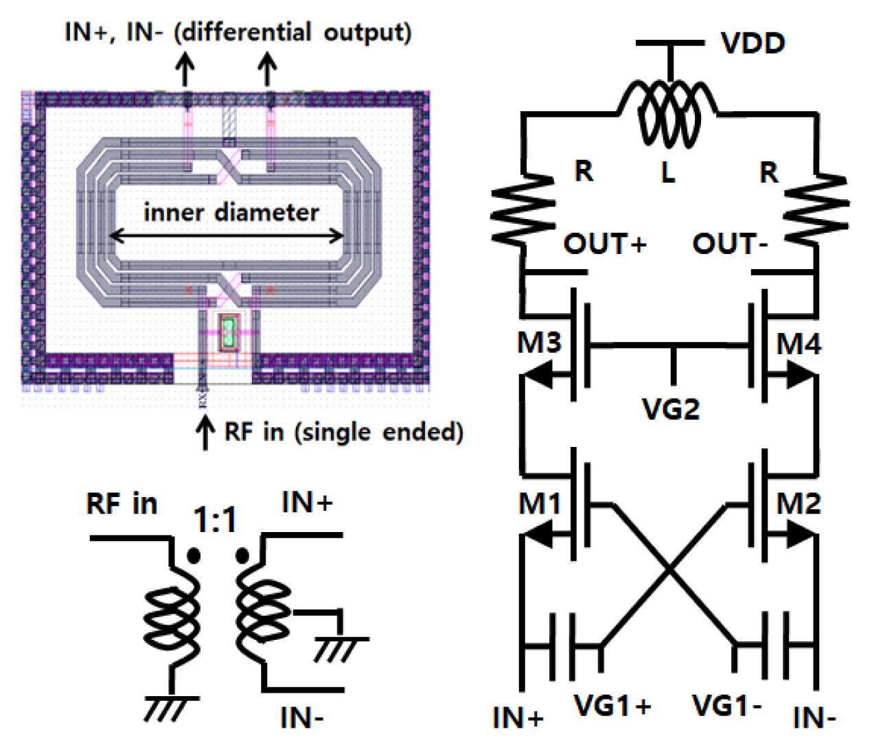
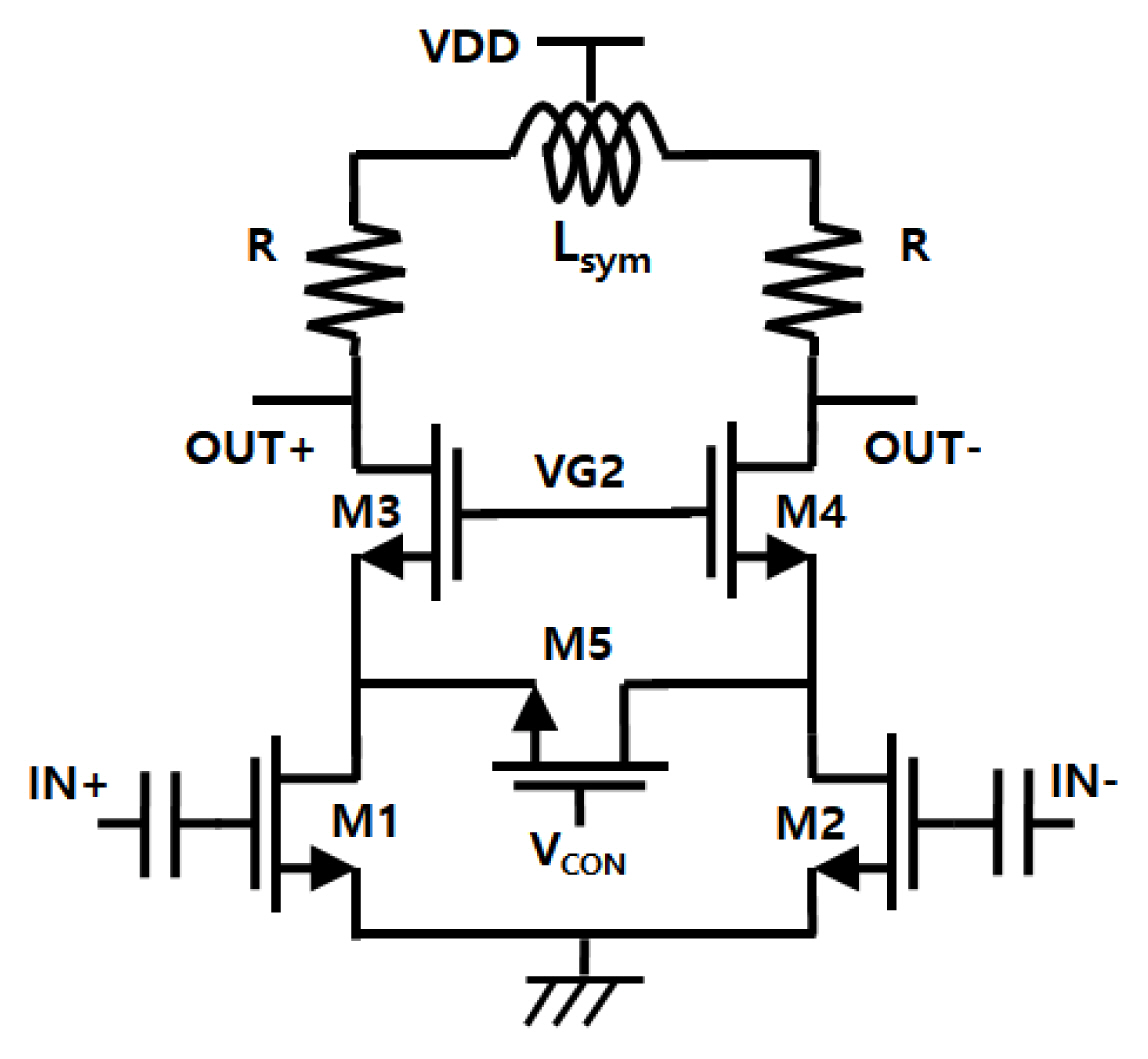
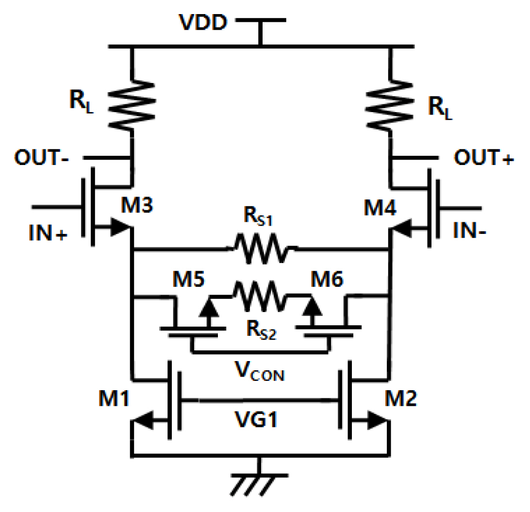
The RF front-end of the receiver is composed of a low noise amplifier (LNA), a three-stage RF VGA, and a down-conversion mixer with a transimpedance amplifier. Fig. 2 shows the circuit schematic of the first LNA stage, which uses the common gate (CG) cascode amplifier with an input single-to-differential (S2D) on-chip transformer. Compared with the single-ended signal, the differential one has a number of advantages, such as robustness to the power supply and substrate noise and reduced even-order harmonic distortion in the integrated circuit. For wideband impedance matching and gain enhancement, the CG input stage is used for the first-stage LNA. In addition, the capacitive cross-coupling CG cascode has a higher transconductance of 2gm and a lower NFmin of 1+╬│/2╬▒ compared with the original CG amplifier [11]. The on-chip transformer is an interleaved structure using the top metal layer for minimum loss. The transformer is designed using a 2.5D EM simulation with the layer parameters obtained from the process layer information provided by the CMOS fabrication company. The on-chip transformer converts the single-ended RF input into the differential output and removes the bulky off-chip balun. The inner diameter, metal width, and metal spacing are 100 ╬╝m, 5 ╬╝m, and 3 ╬╝m, respectively. The three-stage RF VGA also uses an inductive shunt peaking load of R and Lsym for the wideband amplification as in Fig. 3. The RF VGA has a simulated gain control range of 12.3ŌĆō39.7 dB. The final stage of the RF front-end is the adoption of Gilbert cell topology by the down-conversion mixer. Although the sinusoidal LO is used for the LO signal instead of the impulse template waveform, the continuous LO provided by the Tx VCO enables the pseudocoherent receiver operation. The differential output currents of the Gilbert cell mixer are fed to the following TIAs. The down-converted impulse signal, which is the envelope signal and contains the phase term, is amplified and filtered in the following BBA stage. The BBA stage consists of a four-stage VGA, which is the differential resistively degenerated common source (CS) amplifier with the resistive load, as shown in Fig. 4. To cope with the several hundred MHz bandwidth, the conventional Op-amp is not suitable, and the resistively source degenerated CS amplifier is used as the VGA stage. By switching M5 and M6, the source resistance is changed so that the gain can be varied. The simulated 3-dB bandwidth of the BBA stage is up to 610 MHz. The bandwidth of the BBA is determined by the load resistance and the capacitance at the load. To obtain a stable common mode voltage at the output nodes, common mode feedback is used for every amplifier. Moreover, the DCOC loop with low-pass filter amplifier feedback is used to suppress the output DC offset and avoid critical circuit saturation.
The final stage is a differential resistively degenerated CS amplifier for driving the output load. The overall gain and noise figure (NF) of the BBA are 26 dB and 24.2 dB, respectively. The DCOC circuits can remove the input-referred DC offset voltage up to 120 mV in the simulation.
2. Impulse Generator Design for the Transmitter
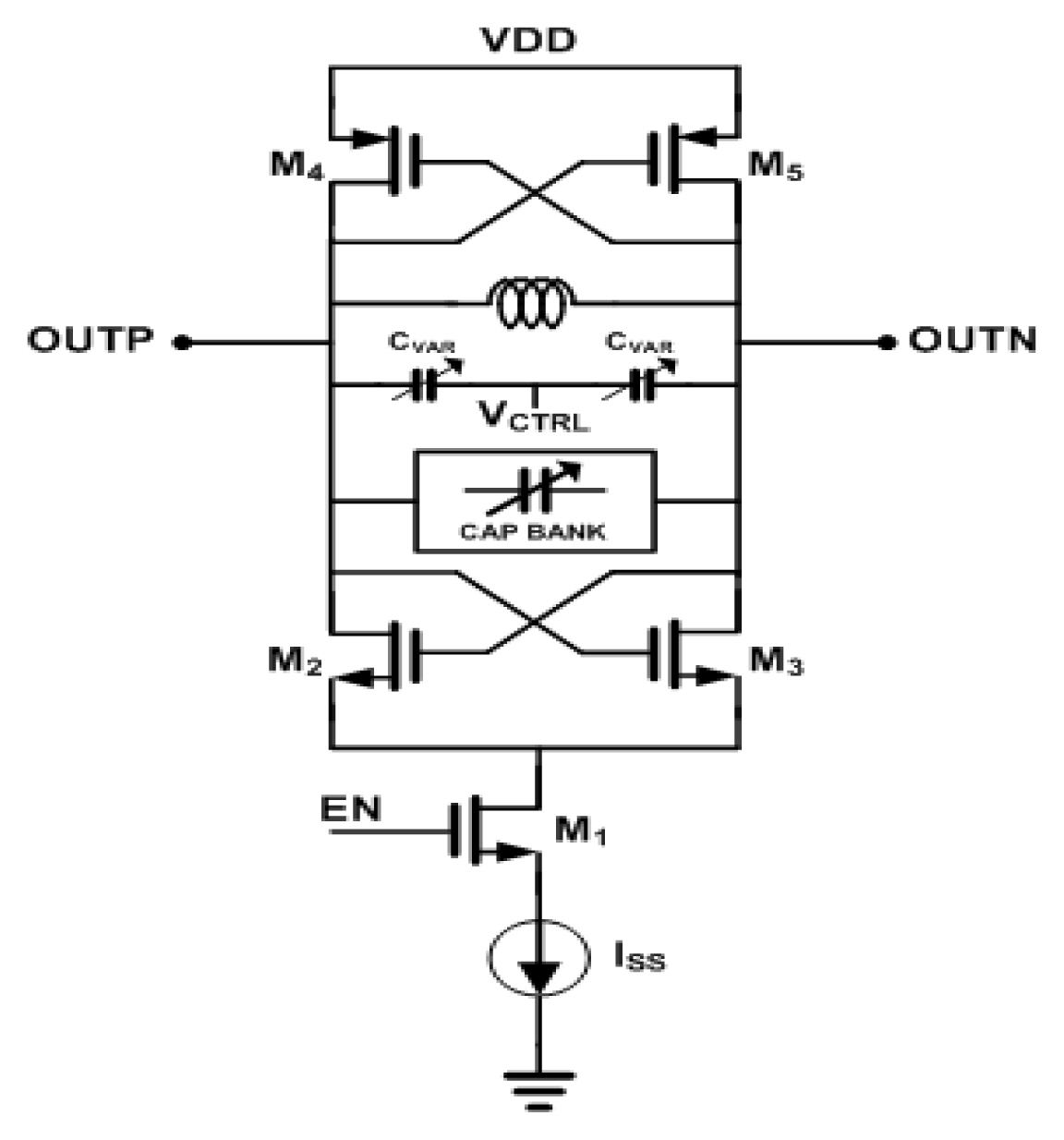
The structure of the UWB transmitter is depicted in Fig. 5. The transmitter includes a digitally adjustable VCO, buffer amplifiers, a control pulse generator for pulse gating and shaping, a switching amplifier, and a driver amplifier. The first buffer amplifier is used to minimize the parasitic load capacitance of the VCO and mitigate the switching noise from the following switching amplifier. Fig. 6 shows the differential cross-coupled LC VCO with a tail current source. The capacitor bank and the control voltage of the varactor can be tuned digitally with the serial peripheral interface.
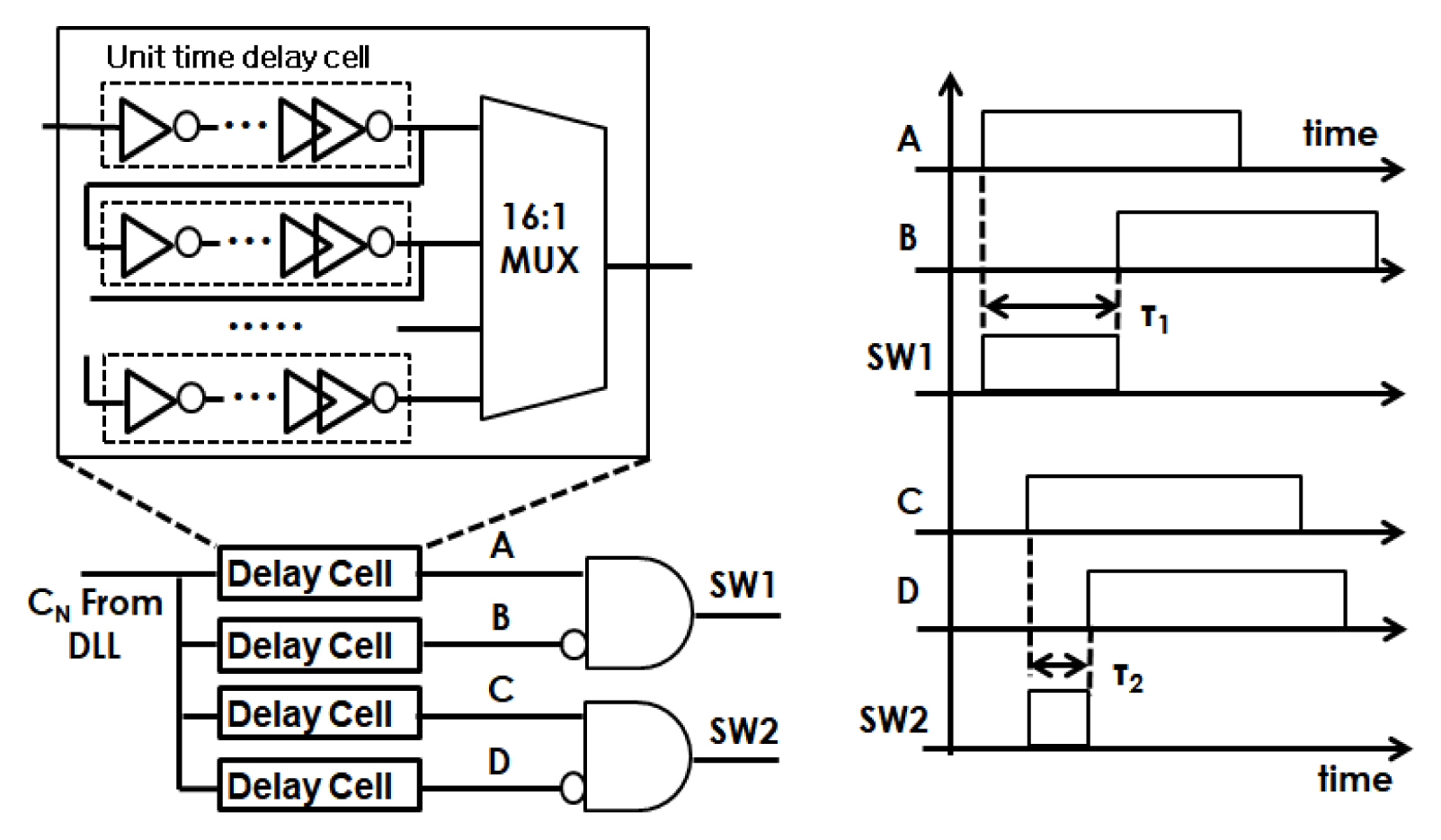
The switching amplifier gates the sinusoidal LO signal by switching the gate bias of the cascode stage with the control pulse signal. The pulse generator provides a control pulse of several ns duration to gate the LO source using the 10 MHz clock coming from the DLL. The output driver amplifier is finally used to provide the 1ŌĆō2 ns short impulse from the gated LO signal and shape the impulse in a triangular-like form. To make the control pulse, the control pulse generator is composed of four delay cells and AND gates. The delay cell contains many unit-time delay cells and a MUX for the timing clock selection, as shown in Fig. 7. By combining the outputs of two delay cells through the XOR gate, the control pulses are generated for switching both the switching amplifier and the driver amplifier.
As shown in Fig. 7, the control pulse for the switching amplifier provides the gated LO signal with a control pulse width of Žä1. On the other hand, the control pulse for the driver amplifier produces a short pulse duration of Žä2. The bandwidth of the transmitting UWB signal is determined by Žä2. The tunable rise and fall times of the gate control voltage result in an impulse envelope with a triangular form using a pulse shaper, thereby reducing the side lobe [8]. The output driver amplifier is switched by the gate bias of the cascode stage, which reduces the power consumption of the mostly power-hungry output driver. The center frequency of the transmitter can be tuned from 6.85 GHz to 9.25 GHz, and its variable BW ranges from 0.8 GHz to 1.3 GHz.
3. DLL Timing Circuit and ADC Design
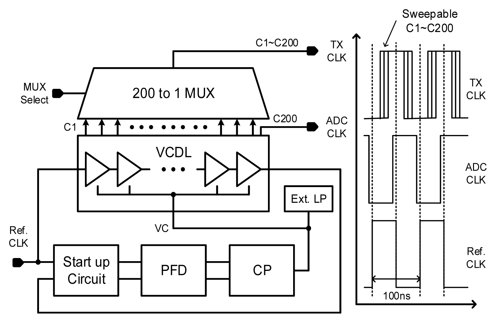
Fig. 8(a) is the block diagram of the DLL generating 200 sampling clocks with an offset time of 0.5 ns for the ETS operation [1]. The DLL includes a chain of voltage-controlled delay line (VCDL) cells, a start-up circuit, a phase-frequency detector (PFD), a charge pump, an external loop filter, and a 200 to 1 MUX. The added start-up circuit prevents incorrect locking [12]. When the reference clock enters, the start-up circuit turns on and wakes up the PFD.
Finally, the total delay time of the VCDL becomes the same period of the reference clock. The VCDL chain consists of 200 VCDL cells, whose outputs correspond to C1ŌĆōC200, respectively. The VCDL outputs of C1ŌĆōC200 are connected to 200 to 1 MUX. The output of the MUX becomes the reference clock for the Tx control pulse generator, and C200 becomes the sampling clock for the receiver ADC. Fig. 8(b) shows the timing diagram.
The ADC is a 6-bit flash-type converter. Considering that the required SNR for the detection is slightly more than 10 dB, 6-bit is sufficient even with some backoff margin. To sample the high-speed impulse waveform, a track and hold circuit is used as the sample and hold circuit of the ADC. In addition, the interpolating technique is used to reduce the number of preamplifiers and comparators, and the bubble-tolerant boundary detector is applied for bubble correction.
IV. Measurement Results
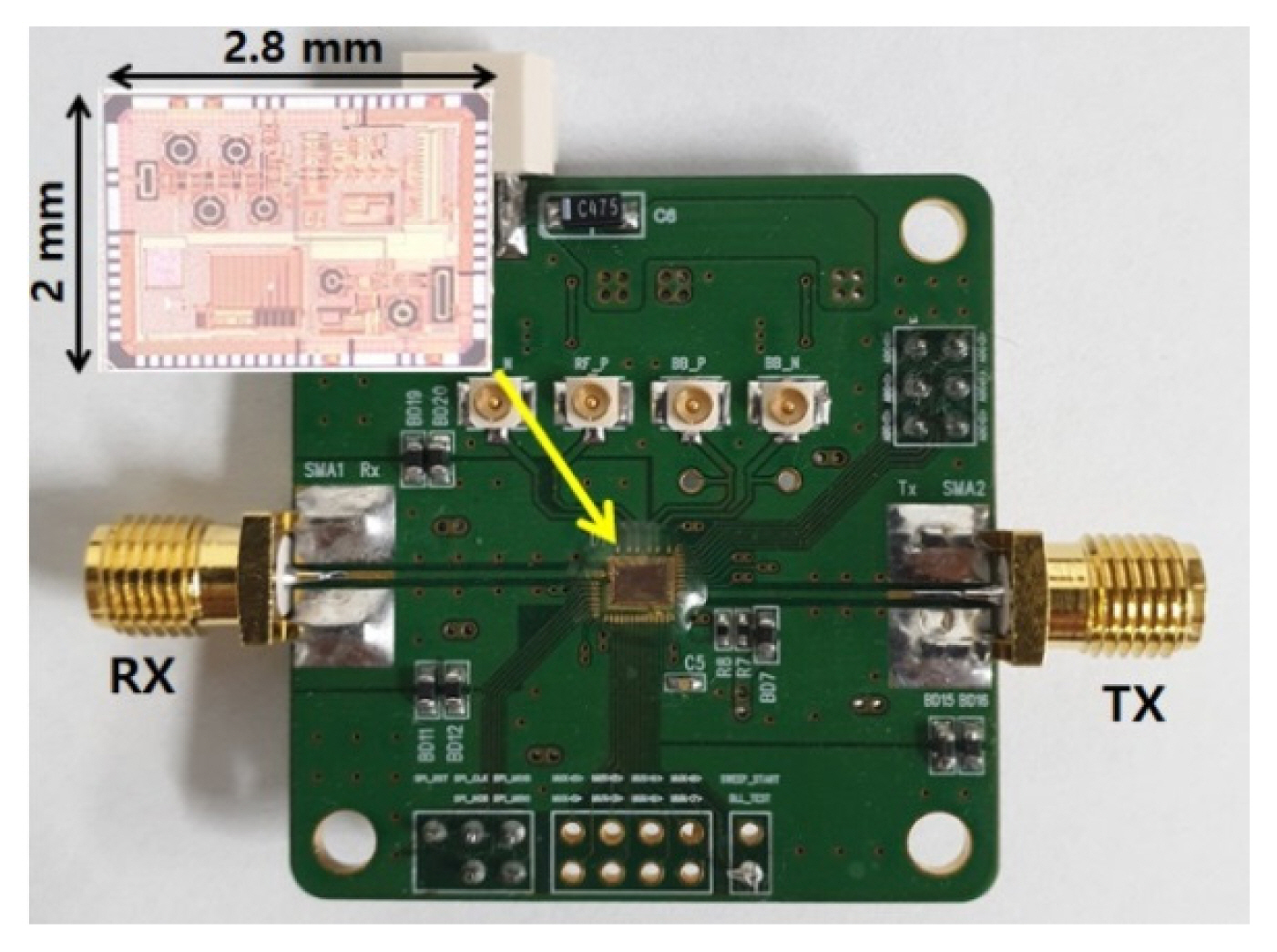
The 7ŌĆō9 GHz UWB radar chip is fabricated using 0.13 ╬╝m CMOS technology. Fig. 9 shows the UWB radar IC and radar module for the measurement. The size of the chip, including the ESD pad, is 2.8 mm ├Ś 2.0 mm. The spectrum of the transmitted UWB signal is measured using a power spectrum analyzer (Agilent E4403A) with a 1 MHz resolution BW. Fig. 10(a) and 10(b) show the results of various bandwidths and three tuned center frequencies, respectively. The bandwidth is defined as ŌłÆ0 dB bandwidth in the UWB system, and the measured bandwidth is from 0.773 GHz to 1.347 GHz. The tunable range of central frequency is 7.5 GHz to 8.6 GHz.
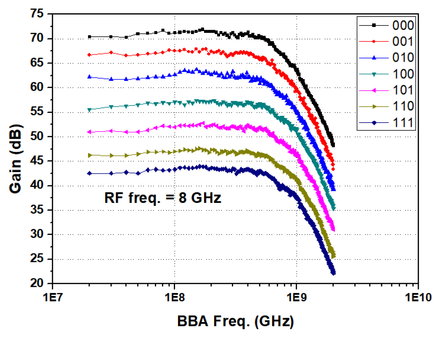
Fig. 11 shows the measured gain of the radar full receiver for each RF gain code. The full receiver gain ranges from 71 dB down to 43 dB with the gain control. As the measured gain range in the BBA stage is also about 20 dB, the full gain dynamic range in both the RF and BBA stages is up to 48 dB. The measured NF at the maximum gain is less than 6.8 dB inside the 500 MHz baseband. The 3-dB bandwidth of the receiver at the baseband output is more than 650 MHz, which effectively corresponds to 1.3 GHz impulse bandwidth. The measured power consumption of the UWB radar IC is 110 mW from a 1.2 V power supply. Table 1 summarizes and compares the performance of our UWB radar IC with that of previously published UWB radar transceivers.
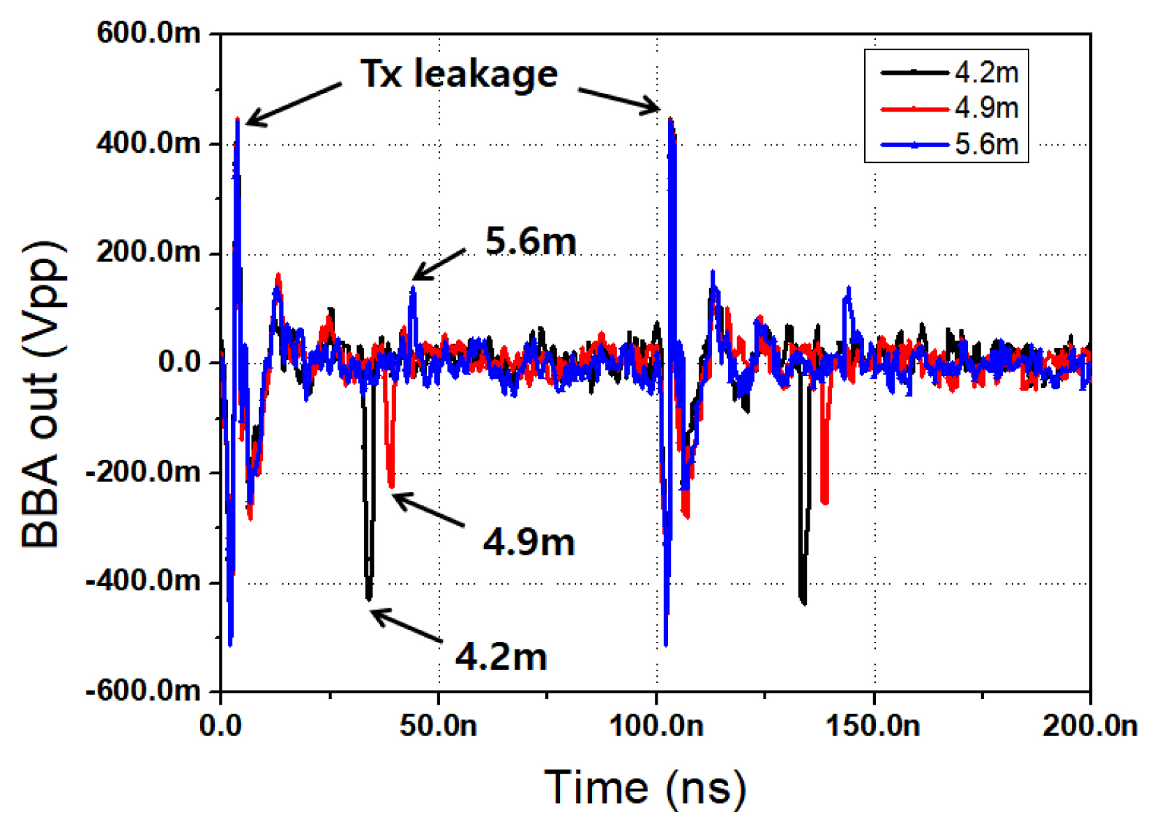
To evaluate the detection range of the radar IC without real noisy channels through the antenna, a Tx to Rx loop-back test is performed while connecting the transmitter directly to the receiver through various lengths of RF cables and a tunable step attenuator. The physical lengths of each cable are 6 m, 7 m, and 8 m. Through measurement of the electrical length of the RF cables with the Vector Network Analyzer, the equivalent lengths in the air of the three cables are found to be 8.4 m, 9.8 m, and 11.2 m, respectively. Because the radar detection distance is half of the wave-propagating distance, the detection distance is recalculated as 4.2 m, 4.9 m, and 5.6 m, respectively.
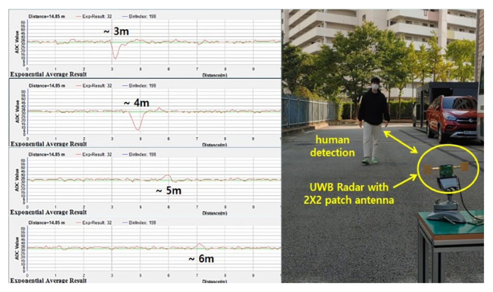
The total loss of the cable and tunable attenuator is set to be the equivalent free-space path loss for each distance, assuming that the antenna gain is 10 dBi, and the RCS is ŌłÆ10 dBsm. Fig. 12 shows the measured receiver output waveform during the loop-back test for each cable length. Around the zero distance, a direct Tx-to-Rx leakage exists, and the received signal in interest is placed at the time delay caused by cable length. The measured results show that the maximum detection range is over 5.6 m. With the help of the signal integration and some SNR enhancement algorithm, the detectable range may be extended beyond 5.6 m. For the real verification of radar performance, a human detection experiment is conducted with 2 ├Ś 2 microstrip patch antennas. The same antenna is used for both the Tx and the Rx, and the antenna gain is 8.1 dBi. The exponential smoothing method for the suppression of static clutters and Tx leakage is applied as a primitive signal processing algorithm. The human detection results in the range of 3ŌĆō6 m are shown in Fig. 13. Although the RCS of the human may vary from time to time, the maximum detection range is more than 6 m, which agrees well with our link budget calculation.
V. Conclusion
A 7ŌĆō9 GHz UWB radar IC was presented for a small and light sensor module. The radar IC used the LO correlation receiver architecture, which had better sensitivity than the self-mixing receiver. The measured detection range for the human target was only up to 6 m with primitive signal processing, and it coincided well with the theoretical link calculation and temporal loop-back test results.