Power Limiter with PIN Diode Embedded in Cavity to Minimize Parasitic Inductance
Article information
Abstract
This letter introduces a power limiter that limits the input power to protect the receiver when a large power enters the radio frequency receiver. When the power limiter receives a large power signal, a positive-intrinsic-negative (PIN) diode is turned on to limit the input power by lowering the impedance. We analyzed the characteristics of the power limiter according to the method of connecting the PIN diode in parallel with the input and output transmission lines of the power limiter. By embedding a PIN diode into the cavity and minimizing the length of the wire, a power limiter was designed and implemented to minimize parasitic inductance. In the S-band, the proposed power limiter’s insertion loss was below 0.5 dB, and the reflection loss characteristics were below 15 dB. Furthermore, it achieved an output P1dB of 21.8 dBm at 3.5 GHz.
I. Introduction
Radio and radar receivers can receive and process extremely small signals. Since the receivers must work well without damage even with a significantly large incident signal, they must be protected by having a power limiter in front of the low-noise amplifier [1–3]. A power limiter consists of DC blocking capacitors, a radio frequency (RF) choke, and a positive-intrinsic-negative (PIN) diode. The RF choke is connected parallel to the signal path of the power limiter. The anode and cathode of the PIN diode are connected to the signal path of the power limiter and ground, respectively. If a considerably large signal is applied to the power limiter, the PIN diode becomes on-state limits the signal, and protects the receiver. However, if a small signal is applied to the power limiter, the PIN diode becomes off-state and must pass through the power limiter without any signal loss.
In this letter, we analyzed the characteristics of the power limiter based on the parasitic inductance generated when connecting the PIN diode. Thereafter, we proposed a structure of a power limiter to reduce parasitic inductance.
II. Analysis of the PIN Diode Connection Method
Fig. 1 shows a simplified circuit diagram of a single-stage power limiter and an equivalent circuit model of a PIN diode in the off-state. LS represents the stray inductance of the bond wires.
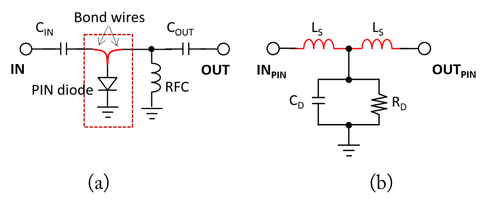
(a) A simplified single-stage power limiter circuit, and (b) an equivalent circuit of a PIN diode in off-state.
When a small signal enters a power limiter, the PIN diode enters the off-state; a power limiter is thus crucial for the lossless transmission of the input signal to the next stage. Fig. 2 shows the simulation results of the insertion and reflection losses in both structures, as the LS is changed by a 0.2 nH interval from 0.2 nH to 1.0 nH when the PIN diode is in the off-state. Here, with reference to Skyworks CLA-4605, CD and RD were applied 0.2 pF and infinity ohm, respectively [4]. CIN and COUT both were applied 100 pF, and RFC was applied 22 nH. We can observe that the smaller the LS, the better the insertion and reflection loss characteristics of the power limiter.
III. Results
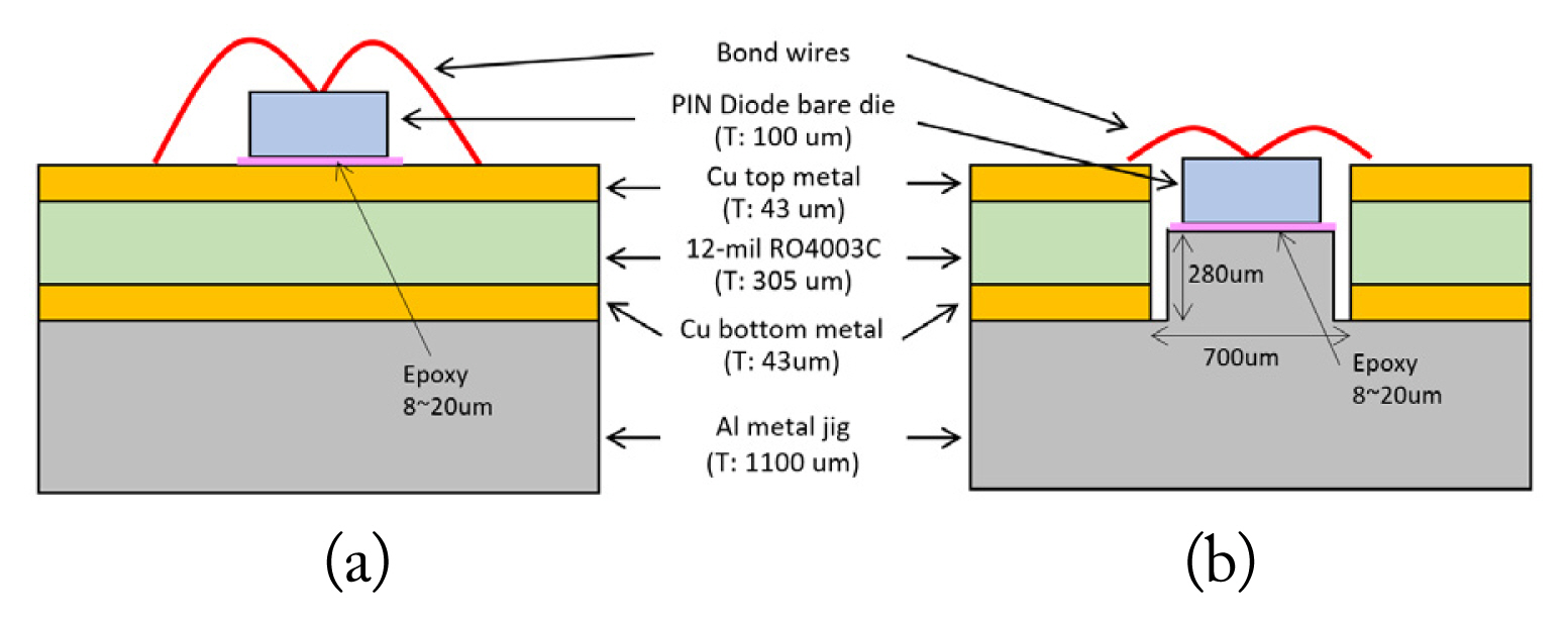
Typically, a packaged PIN diode [4] is applied to a power limiter. However, it adds parasitic inductance and capacitance due to the packaging, and it degrades the power limiter performance. Therefore, we employed the bare die of the PIN diode directly into the power limiter and proposed a cavity structure to minimize parasitic components. Fig. 3 shows the cross-sectional views of the conventional and proposed structures to minimize the parasitic inductance caused by connecting a PIN diode to a power limiter. The proposed structure can minimize the length of the bond wire by equalizing the height to the signal path of the power limiter and the anode of the PIN diode [5, 6]. A 700-μm hole was formed to embed a PIN diode in the PCB. The heights of the PIN diode and substrate were adjusted to the convex structure of the metal jig bonded under the substrate. The bond wire had a length of approximately 400 μm, which was approximately 200 μm less than that of the conventional structure (600 μm).

Cross-sectional view of (a) conventional and (b) proposed structure for a PIN diode connected to a power limiter.
The PIN diode used in the power limiter was made of a six-inch silicon wafer using the Electronics and Telecommunications Research Institute’s infrastructure. Fig. 4 shows photographs of the six-inch silicon wafer and a bare die having a size of 460 μm × 460 μm, and the measurement results of the PIN diode’s bare die. The breakdown voltage of the PIN diode is 73 V, and the junction capacitance (Cj) at a frequency of 1 MHz is 0.113 pF at a cathode voltage of 0 V.
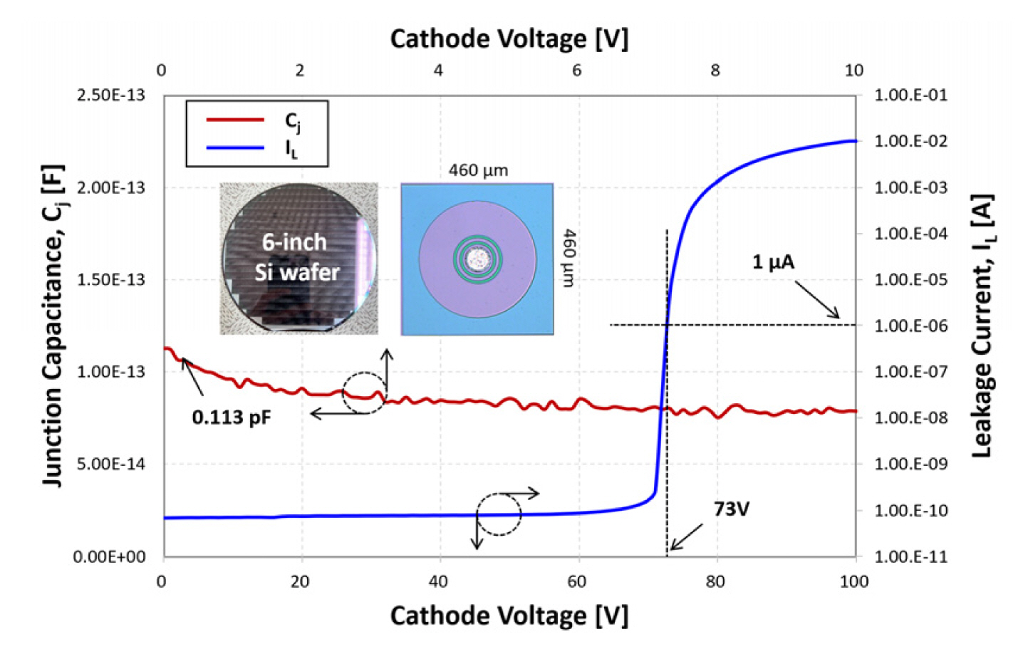
Photographs and measured junction capacitance and reverse breakdown voltage characteristics of the implemented PIN diode.
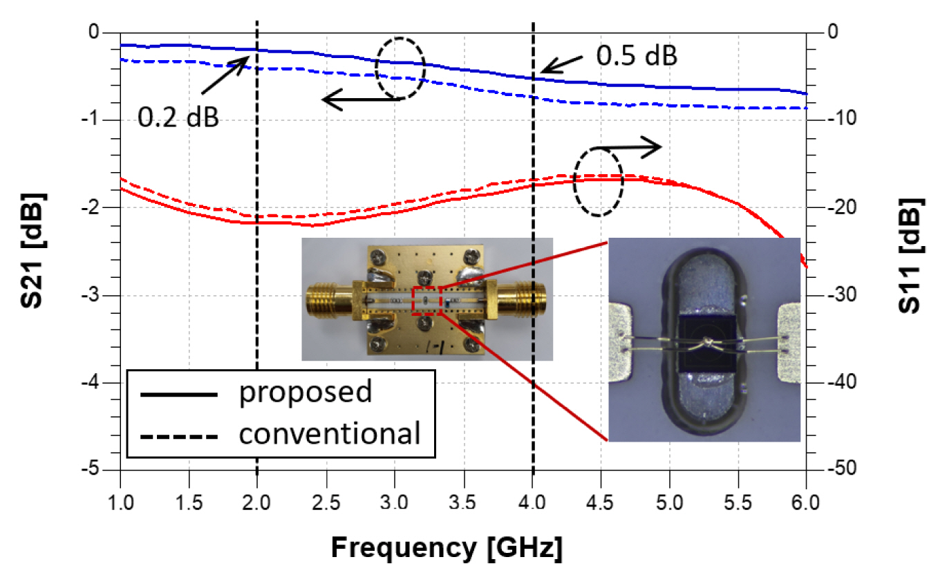
Two power limiters with conventional and proposed structures were fabricated using a 12-mil RO4003C substrate with a copper metal of 1/2 oz. Fig. 5 shows a photograph of the power limiter fabricated using the proposed structure. The PIN diode is embedded in the cavity of the substrate and then connected to a bond wire with a minimum length of 400 μm. Because the anode diameter of the PIN diode is 40 μm, a gold bonding wire with a diameter of 20 μm was used to connect each side to the input and output, as shown in the enlarged photo in Fig. 5. Furthermore, Fig. 5 shows the measured S-parameters of the two power limiters, and it is evident that the parasitic inductance owing to the bond wires affects the insertion and return losses of the power limiter.
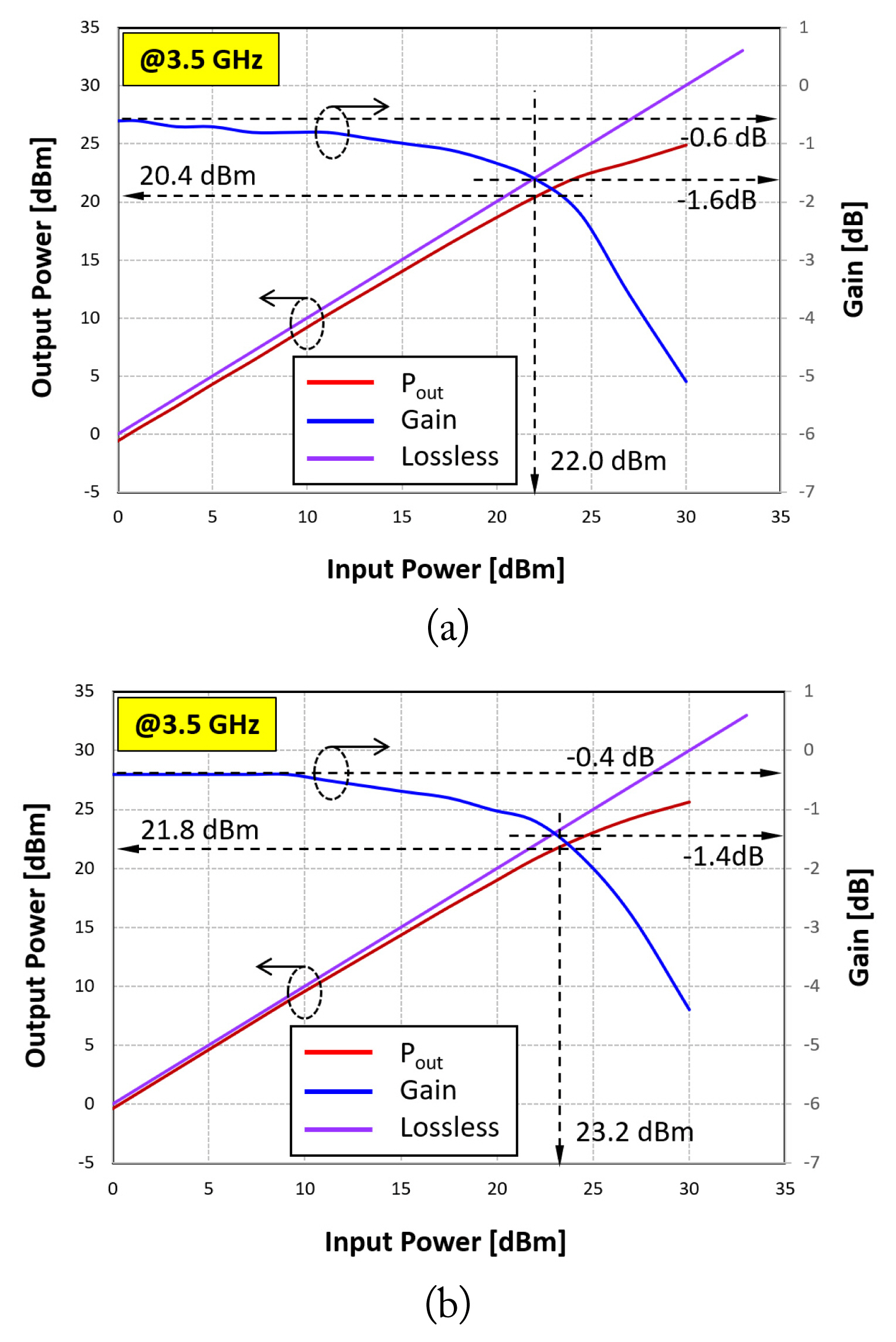
Fig. 6 shows the characteristics of the output power as a function of the input power for the conventional and proposed power limiters. The pulsed-input signal has a pulse width of 10 μs and a duty cycle of 1% at a frequency of 3.5 GHz. The power limiters using the conventional and proposed structures have an insertion loss of 0.6 dB and 0.4 dB, respectively, and an output P1dB of 20.4 dBm and 21.8 dBm, respectively.
IV. Conclusion
We analyzed the PIN diode connection structure in a power limiter to protect the RF receiver, and we proposed a structure to minimize the parasitic inductance. The power limiter using the self-developed PIN diode showed an insertion loss of less than 0.5 dB at S-band (2–4 GHz) and an output P1dB of 21.8 dBm at 3.5 GHz.
Acknowledgments
This material is based upon work supported by the Civil-Military Technology Cooperation Program (No. 19CM50 79) and by the National Research Council of Science & Technology (NST) grant by the Korea government (MSIT) (No. CRC-19-02-ETRI).
