I. Introduction
Broadband array antennas with low mutual coupling have attracted a lot of attention due to their various industrial applications. However, there are two main challenges in the implementation of these array antennas. First, it is difficult to achieve a reduction in mutual coupling between the antenna elements over a wide bandwidth. Second, in many cases, the antenna arrays operating over a wide impedance bandwidth have three-dimensional structures that are difficult to implement [1]. One of the critical problems in the implementation is to obtain a reliable electrical contact between the feed lines and the SMA connector by soldering. In fact, the problem is aggravated in large arrays designed to operate at high frequencies, such as the Ku-band. Additionally, in large arrays, there is a considerable risk of rejection if, after the fabrication, some of the antenna elements are found to be defective. Therefore, to overcome these challenges, the implementation of a modular array antenna that can easily replace the faulty antenna elements is required, especially for large arrays.
Owing to their reconfigurability, the modular array antennas have an additional advantage for the development of array structures for microwave radar systems. In the case of developing an imaging radar, there is no definite solution to determine the optimal positions of the TX and RX antenna elements for the acquisition of the best scattering data from the target due to the dynamic range and direction of the target [2]. Moreover, the reconfigurable array structures can be experimentally used to control the radiation patterns of the arrays and reduce the number of antenna elements in an array using the array thinning technique [3]. In previous research, a wideband modular array was studied, but it had high mutual coupling [4]. In this study, a wideband and low mutually coupled modular array antenna is proposed. The individual antenna element of the proposed array is designed using the methodology reported in [1].
II. Design of Array Antenna Structure and Operation
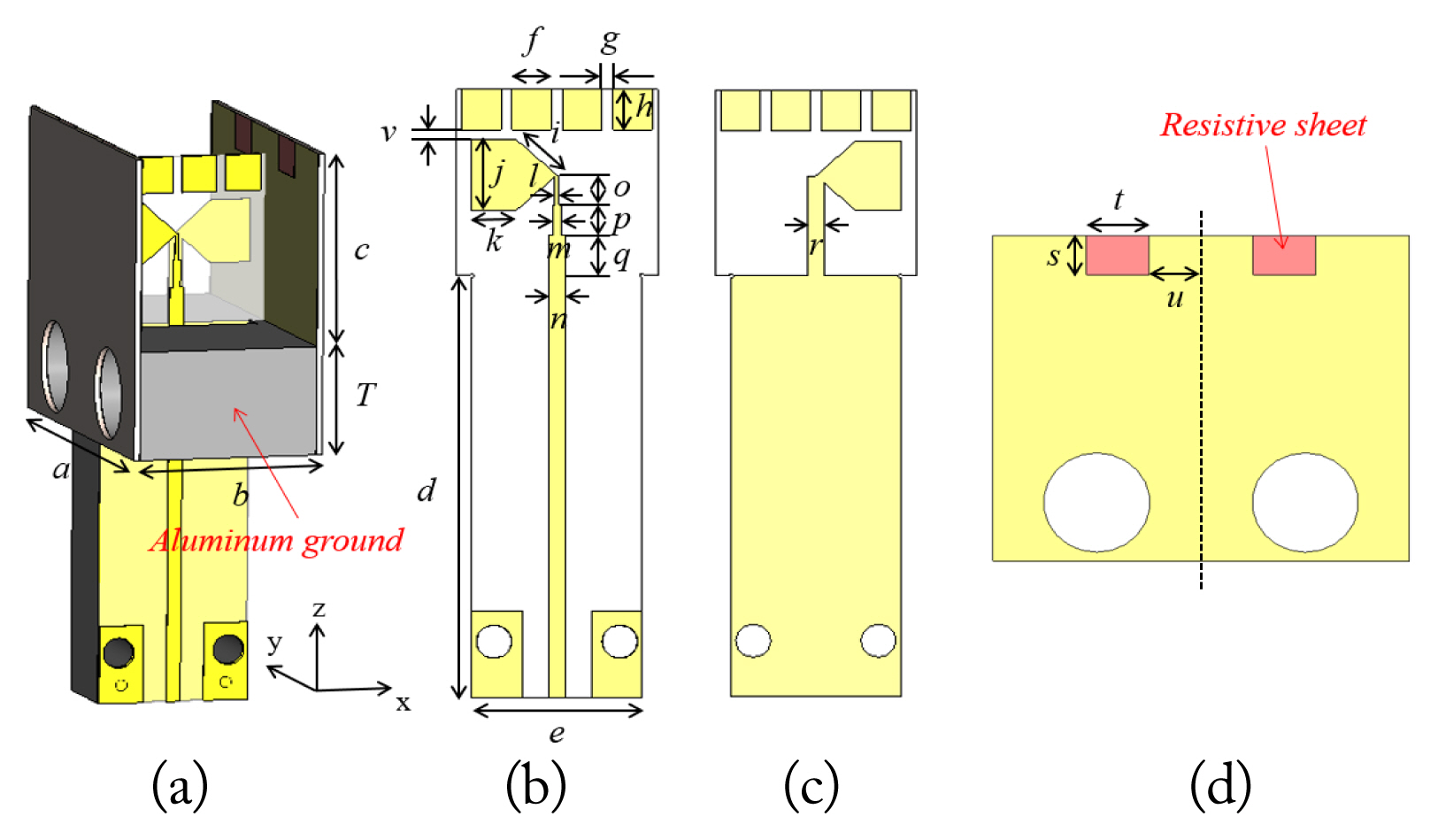
To implement the wideband array antenna, grounded electrical side walls must be tightly coupled to the tips of the dipole arms, as shown in Fig. 1(a), and the frequency-selective surface (FSS) in Fig. 1(b) should have proper patch sizes f, g, and h (Table 1). The FSS replaces the dielectric superstrate in [1] and is more suitable for modular unit cells due to its light weight and compactness but has the same electromagnetic effect as the dielectric superstrate. Furthermore, the positions and sizes of the resistive sheets determine the quantity of mutual coupling between the antenna elements and the radiation efficiency. The determination of the positions and sizes and a parametric study are described in detail in [1]. The modified unit cell structure consists of side walls, a printed circuit board (PCB), and an aluminum ground, which can be assembled or detached. Fig. 1(a) shows the assembled structure of the proposed antenna element. It features a T-shaped aluminum ground, and the vertical part of this ground structure provides a mechanical support for the PCB from the back. The horizontal part of the ground is slotted in the center to insert the PCB. Two holes are used to insert the aluminum rods, as shown in Fig. 2(b), to fix the unit cell structures. On the bottom side of the PCB, there are two holes for using the end-launch connector (https://www.with-wave.com/end-launch-narrow-block). The PCB is a Taconic TLY-5 (╔ør = 2.2, tan╬┤ = 0.0009) with a thickness of 0.25 mm. The simulated resistive film was 250 ╬®/square (https://ohmega.com/) and it as laminated on the side wall with FR-4 (╔ør = 4.3, tan╬┤ = 0.025).
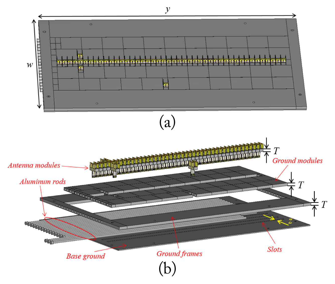
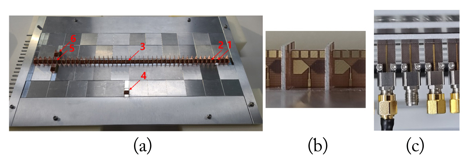
Fig. 2(a) shows the proposed 47 antenna elements assembled on a 46 ├Ś 9 ground board. The ground modules, which have two different sizes, fill the positions where there are no antenna modules present. The antenna modules, which are arrays designed using the proposed single element shown in Fig. 1(a), are inserted through the slots of the base ground. As shown in Fig. 2(b), the aluminum rods fix the entire structure by passing through the side holes of the ground frames, antenna modules, and ground modules, and this is the final step of the assembly. The right ends of the rods and the right side of the ground frame are bolted together. The fabricated array antenna is shown in Fig. 3. In this study, only the performances of six ports are presented as a representative, as shown in Fig. 3(a).
Fig. 4 shows the simulated and measured S-parameters of the six ports. For ports 5 and 6, the simulated and measured mutual coupling was slightly larger than ŌłÆ20 dB at 12 GHz, and the others were lower. Thus, the active reflection coefficient at port1 is similar to S11. Moreover, the simulated and measured reflection coefficients are below ŌłÆ10 dB at the Ku-band. The simulated and measured active element gains at 12, 15, and 18 GHz are shown in Fig. 5. The beamwidth in the E-plane was approximately 120┬░ and 160┬░ in the H-plane. The radiation efficiency and broadside gain are presented in Fig. 6. The simulated efficiency is greater than 65%, and the measured efficiency is greater than 52%. The simulated gain is greater than 2.2 dBi, and the measured gain is larger than 1 dBi. The difference between the simulation and the measurement is considered to be due to the fabrication error: the height s of the fabricated optimized resistive film for low mutual coupling is 3 mm, and not 2 mm.
III. Conclusion
In this paper, a modular array antenna was proposed with a low mutual coupling in the entire Ku-band. It was proposed that, by dividing the entire structure into modules, a simple mechanical assembly is enough to fabricate any antenna array structure without the need for soldering. The paper also offered a reliable fabrication method for implementing large array antennas. With the proposed structure, it is possible to replace the faulty antenna elements in the large arrays and to experimentally test various array designs without the requirement for the repeated fabrication of different array patterns. This is because the antenna modules can be put into desired locations on the ground frame.


