


I. Introduction
The sixth-generation (6G) of wireless communication aims to achieve ultra-high data rates (up to 1 Tbps), ultra-low latency, high energy efficiency, ubiquitous global network coverage, and intelligent connectivity all over the world [1]. The millimeter-wave frequencies, especially in the D-band, are promising candidates for 6G applications. Similar to other frequencies, the D-band on-chip transceivers will also be integrated with printed circuit boards (PCBs). Since millimeter-wave equipment, such as vector network analyzers (VNAs) and upconversion mixers, typically employs hollow metallic waveguides (WGs), the WG-PCB transition is required. Another potential application of the transition is the testing of PCB-based millimeter-wave passive circuits, circuits, such as antennas, filters, and power dividers. In the open literature, various WG-microstrip line (MSL) transitions have been reported [2–6]. In [2], a vertical WG-differential MSL (DMSL) transition was reported, in which bandwidth was enhanced using a short-end parasitic patch. In [3], Chebyshev-based vertical impedance transformers were designed in the WG section and connected to a DMSL, which does not require a backside cavity, as in [2]. In [4], a wide-band transition was designed by combining an E-plane probe and an MSL transition that covered the whole W-band. The authors in [5] designed Chebyshev-based impedance transformers in a rectangular WG (RWG) connected to a tapered MSL by extending a substrate into the RWG. Hugler et al. [6] presented a WG-DMSL inline transition on a multilayer substrate with a −10 dB impedance bandwidth (IBW) of 30 GHz. The reported works [2–5] require modified WG parts that increase the overall size and fabrication cost. In [6], the use of a multilayer substrate with WG parts made the proposed design expensive.
The substrate integrated waveguide (SIW) technology has also been investigated for WG-PCB transitions [7–11]. SIW-based transitions are generally divided into two categories. In the first category, tapered structures are designed to couple energy from the WGs that achieve wide bandwidth at the cost of large size and expensive fabrication [7–11]. In [7], a tapered SIW line with an extended dielectric substrate was utilized that produced a −10 dB IBW of 40 GHz (75–115 GHz). In [8], a W-band linearly flared antipodal slot line was inserted into the WG for coupling energy to an SIW line designed on a multilayer liquid crystal polymer (LCP) substrate. A fin-line coupling structure was reported in [9] for designing a WG-SIW transition that obtains a −10 dB IBW of 40 GHz (110–150 GHz). The second type uses slots to directly couple the energy from the WG, which is compact but has a relatively narrow bandwidth. A two-layer configuration was used in [10] and [11] for W-band applications. In [10], the upper layer has a slot-embedded patch to couple energy from the WG. A rectangular coupling slot was utilized to couple energy from the upper to the lower SIW, and a −10 dB IBW of 18.8 GHz (85.7–104.5 GHz) was obtained. In [11], a magneto-electric (ME) dipole was placed under the WG on the top substrate, while a bowtie slot coupled energy from the top to the bottom SIW. The measured −10 dB IBWs were 16.9 GHz (68.4–85.3 GHz) and 20.7 GHz (68.6–89.3 GHz) for the 5-mil and 10-mil RO3003 substrates, respectively.
In this work, we designed a WG-SIW transition based on the second type by using only a single layer substrate. The WG couples energy to a SIW cavity through a rectangular slot. The designed cavity has three vias at the back of the cavity, which are arranged in the form of a triangle. The investigation of the proposed cavity based on the eigen-mode simulations reveals that the TE320 mode is excited at 126 GHz and 142 GHz. The TE320 mode is also shown to be excited at 126 GHz for the isolated rectangular cavity (which does not have the triangular vias arrangement at the backside). However, the same mode at 142 GHz arises only in the proposed isolated cavity. For actual transition implementation, two initial designs, namely Trans-I and Trans-II, are compared, which differ only by the use of matching vias. The E-field comparison inside these transitions shows that the matching vias assist in maintaining TE320 mode distribution at 142.8 GHz, which is the transmission null point for Trans-I. Although the transmission null has been moved to 156.6 GHz, the −10 dB IBW occupies only 6 GHz (126–132 GHz). This is indeed a narrow band in the D-band. Therefore, a parasitic rectangular patch is embedded at an optimized location inside the coupling slot to broaden the −10 dB IBW. The −10 dB IBW was improved from 6 GHz to 27.4 GHz (127.2–156.4 GHz) using the parasitic patch. The performance of a back-to-back transition is experimentally shown to yield a broad −10 dB IBW of 26.5 GHz (135–161.5 GHz). It is worth mentioning that there are two earlier studies [12, 13] concerning the use of single-layer substrate transitions. In [12], a thick metal cladding was used in the design, which increased the complexity, loss, and cost of the transition. Furthermore, a conventional cavity was used to support TE120 and TE320 modes in the frequency of operation, while our proposed cavity supports TE320 modes at two different frequencies [12]. A wide-band transition with a simulated −10 dB IBW of 30.3 GHz (47.2–77.5 GHz) was reported in [13]. The design utilized a conventional rectangular SIW cavity on a 0.508 mm-thick substrate, but the explanation of the cavity modes was not given [13].
In the proposed work, a comparable −10 dB IBW was achieved using a novel modified cavity that is shown to support the TE320 at more than one frequency. The new features of the proposed cavity compared to the conventional cavity are discussed based on the TE-mode analysis by the eigen-mode simulations as well as calculations. The role of matching vias based on the effect on the TE mode is also discussed. The details of the SIW transition with a parametric study and measurement results are detailed in Sections II and III, respectively.
II. SIW Transition Design
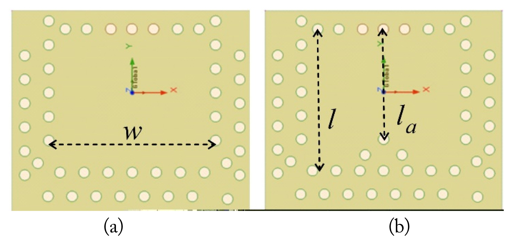
Fig. 1 depicts the geometry of the SIW-based transition that is realized on a 0.254-mm thick Rogers Duroid 5880 substrate with a relative permittivity ɛr = 2.2. The SIW cavity is formed by shorting the top and bottom metal of the PCB through several vias. Each via has a diameter d and a center-to-center distance of p. The coupling SIW cavity has length and width of l and w, respectively. A slot of dimensions a × b is etched from the bottom metal such that the length and width are the same as that of a standard WR6 WG. A small inner patch of length lp and width wp is placed inside the slot, with a gap of g from the nearest bottom metal.
A via at the backside of the cavity has spacing s from the edge of the slot. The positions of the backside vias were optimized using HFSS software. A SIW line with edge-to-edge width of c is used at the output of the SIW transition to couple the energy.
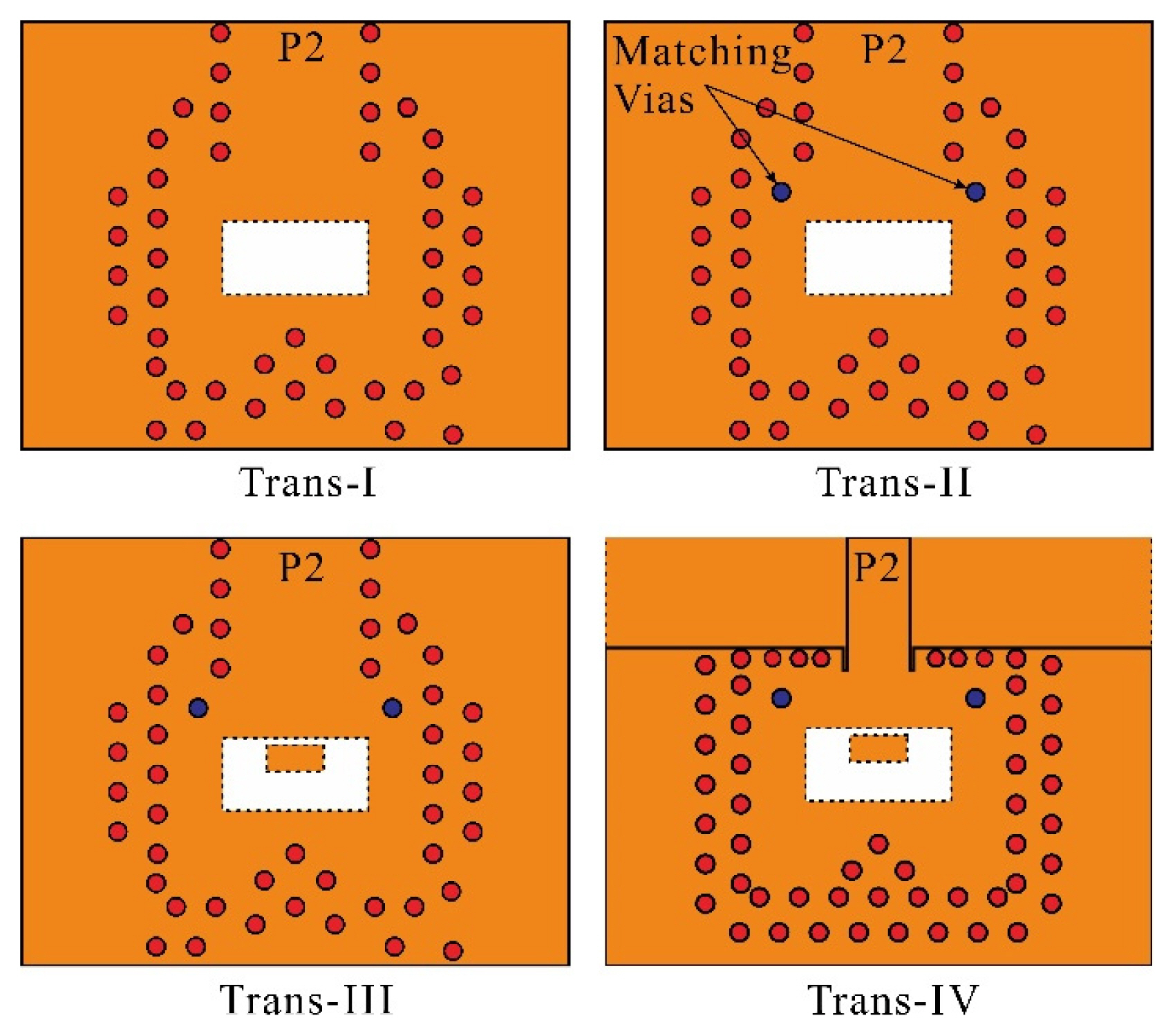
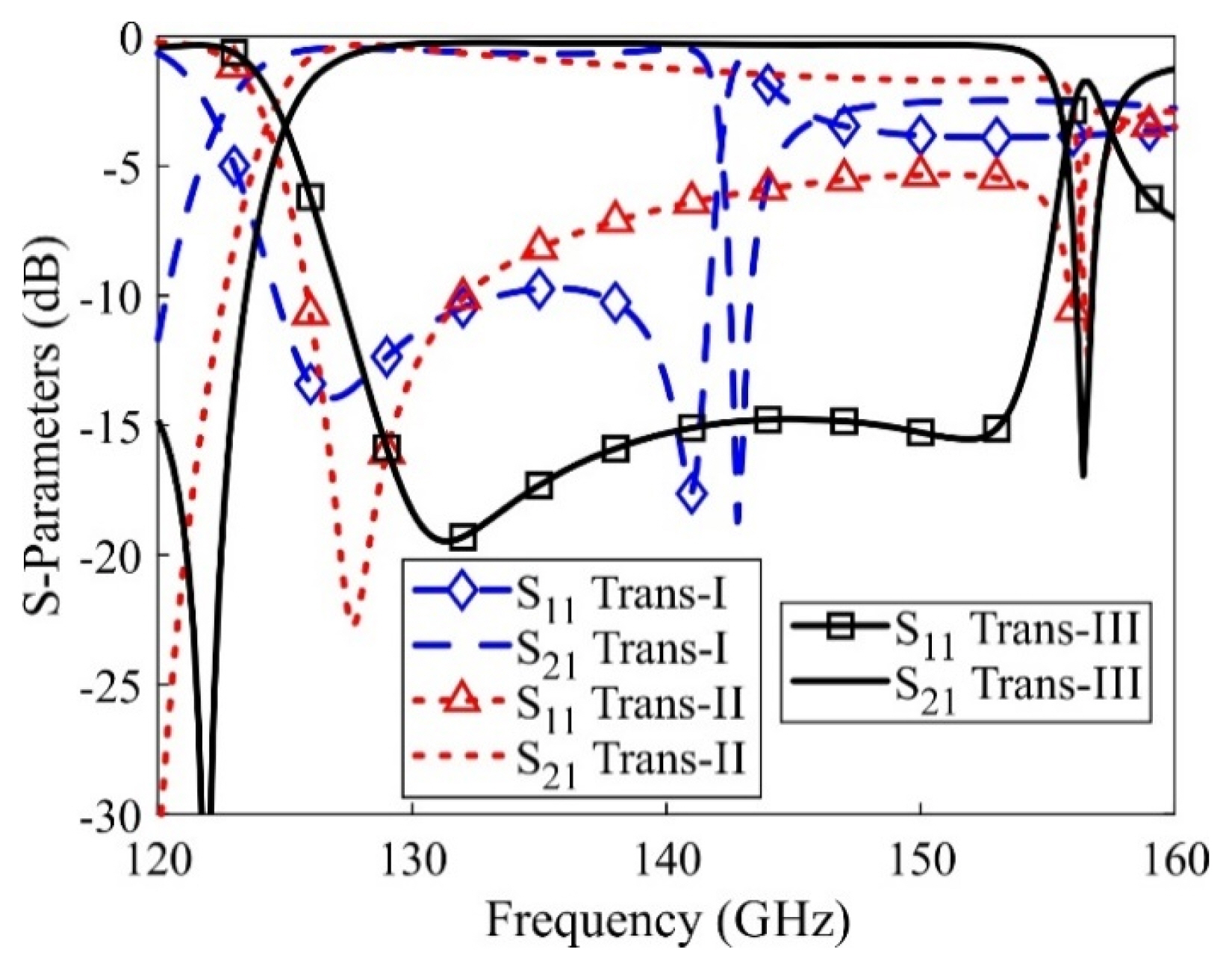
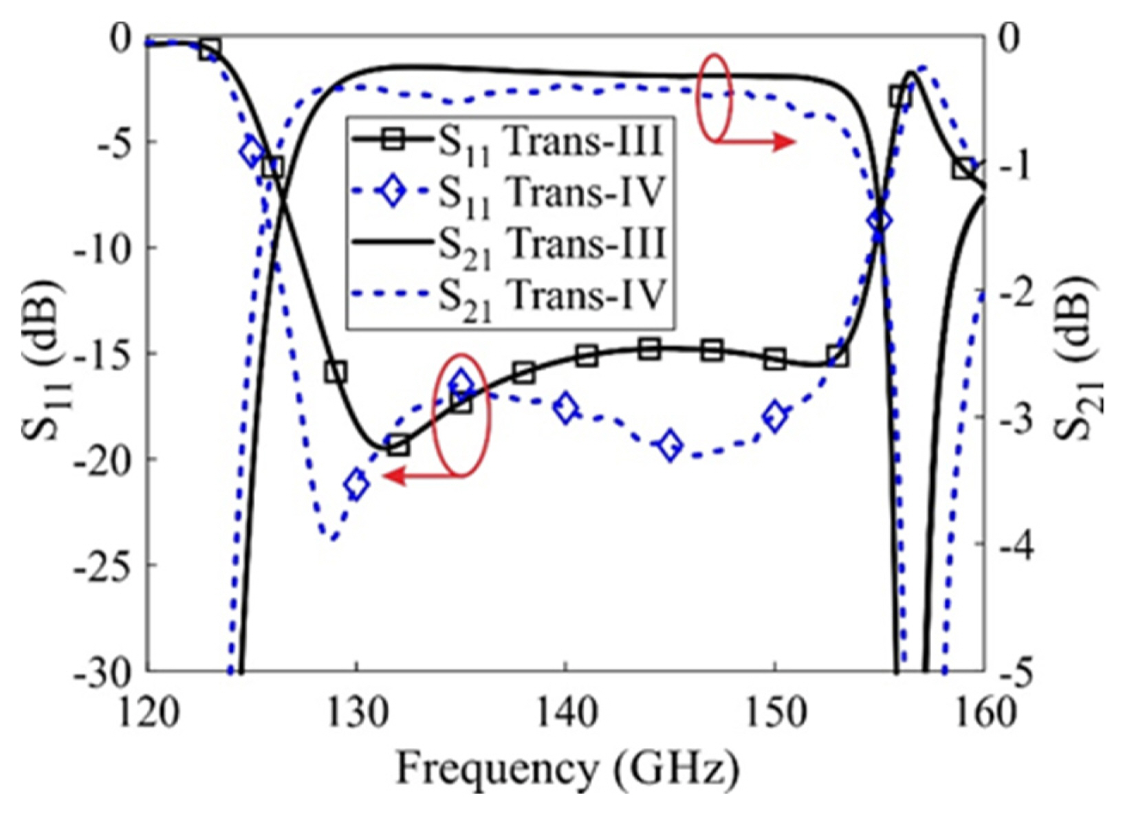
Fig. 2 shows the geometries of four transitions (Trans-I, Trans-II, Trans-III, and Trans-IV) to elaborate the final design. A comparison of the simulated transmission and reflection coefficients of the first three is depicted in Fig. 3. Trans-I is a simple cavity without matching vias and an inner patch. The simulated results from Fig. 3 show a −10 dB IBW of 8.6 GHz (124.81–33.4 GHz) and a 3 dB BW of 29.7 (112.3–142 GHz). By inserting a pair of matching vias, the inband null is shifted from 148.2 GHz to 156.6 GHz, and the transition is termed Trans-II. However, impedance matching is poor above 132 GHz, as observed for the −10 dB criterion. A rectangular parasitic patch of optimized dimensions is added to Trans-II and termed Trans-III. As a result, the simulated −10 dB IBW to 27.4 GHz (127.2–156.4 GHz) and 3 dB BW of 30.4 GHz (125.1–155.5 GHz) were achieved.
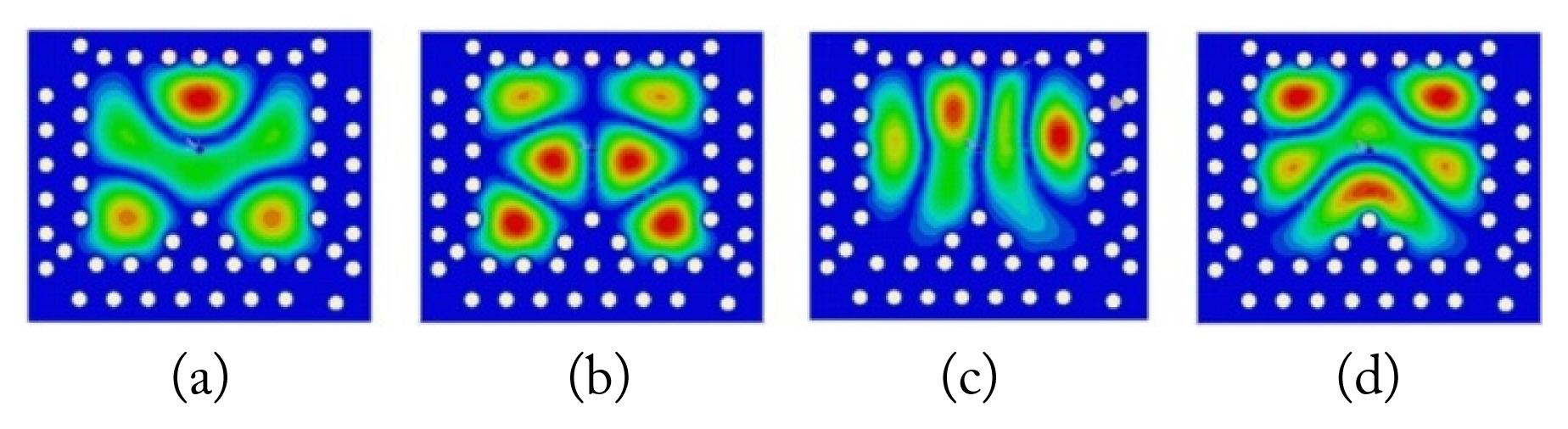
It is well known that the SIW cavities support TEmn0-modes. The working of the proposed transition can be elaborated by addressing the TEmn0-modes involved in the operation; therefore, we performed an eigen-mode analysis of the isolated conventional and proposed SIW cavities. The geometries of these designs are depicted in Fig. 4. The rectangular cavity was designed by removing the triangular vias from the proposed cavity. The simulated results of the resonance frequencies along with the E-field distributions of Mode-1, Mode-2, Mode-3, and Mode-4 are plotted in Fig. 5. The E-field of these modes in ascending order of frequencies resembles those of the TE320, TE230, TE410, and TE330, respectively. The resonance frequencies of these TE modes can be calculated using Eq. (1):
where m, n denotes the indices of the excited mode, c is the speed of the light, and ɛr is the relative dielectric constant of the substrate. leff and weff are given by
where d represents the diameter of a via and p denotes the periodicity of the via array. The calculated resonance frequency
values of Mode-1, Mode-2, Mode-3, and Mode-4 were 126.8 GHz, 134.2 GHz, 139.2 GHz, and 153.6 GHz, respectively. The maximum difference between the simulated and calculated values was 1.6%. Next, we performed the eigen-mode analysis of the proposed cavity and the resonance frequencies along with the E-field distribution for the first four modes are plotted in Fig. 6. By comparing the individual distributions in Fig. 6 to those in Fig. 5, we observed that at 126 GHz, the field distribution resembled Mode-1 of the isolated rectangular cavity, although not exact and, therefore, we termed it quasi-TE320 mode. Mode-2 in both cavities looked alike, whereas Mode-3 in the proposed cavity was slightly different from that of the isolated rectangular cavity. The main difference appeared in Mode-4, as the proposed cavity design excites a quasi-TE320 mode at 142 GHz as well. The resonance frequency of Mode-4 can be accurately calculated assuming the length of the proposed cavity la = l − 2 × p + 1.5 × d given in (2). Based on this comparison, we conclude that unlike the conventional cavity, the proposed cavity supports another quasi-TE320 mode while the other first three modes (Mode-1, Mode-2, and Mode-3) look similar.
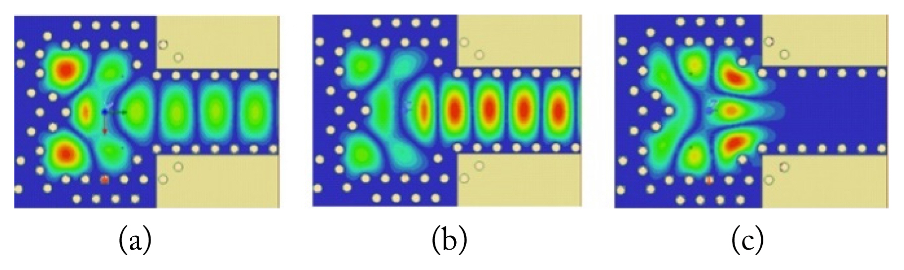
To explain the purpose of the matching vias, we plotted the E-field distribution inside Trans-I and Trans-II at the resonance and null points as shown in Figs. 7 and 8, respectively. As shown in Fig. 7, the TE320 mode was excited at 126.8 GHz. The second resonance point (140.8 GHz) occurred close to the null point (142.8 GHz) of Trans-I; therefore, the field distribution inside the cavity showed resemblance. For Trans-II, the lower resonance point occurred at 127.8 GHz, and the field distribution verified the excitation of TE320 mode. By comparing Fig. 7(c) with that of Fig. 8(b), we observed that the use of matching vias induced TE320 mode in Trans-II; therefore, the power flowed inside the connected SIW line. The null forming point was shifted to 156.8 GHz, which had the same E-field distribution as in Fig. 7(c). The field distributions in Figs. 7 and 8 also inform an interesting conclusion; that is, only TE320 modes are utilized in the proposed design.
Next, we demonstrated the performance comparison between MSL and SIW, which were separately connected with the WG-SIW transition to couple the energy. This transition to MSL is termed Tran-IV. It is worth mentioning that the dimensions of the SIW cavity are the same in both designs for a fair comparison. The comparative simulated results are displayed in Fig. 9. Trans-IV obtained a −10 dB IBW of 28.4 GHz (126.2–154.6 GHz), which is a little wider than Trans-III. However, Trans-III was chosen for fabrication due to its lower loss.
We also performed a parametric study concerning the effect of variations in gap g on the simulated S-parameters, as depicted in Fig. 10. We observed that the lower resonance shifted toward the higher frequency side, and impedance matching improved with a decrease in the value of g. The best result was obtained for g = 0.08 mm, which was the minimum limit of precise fabrication.
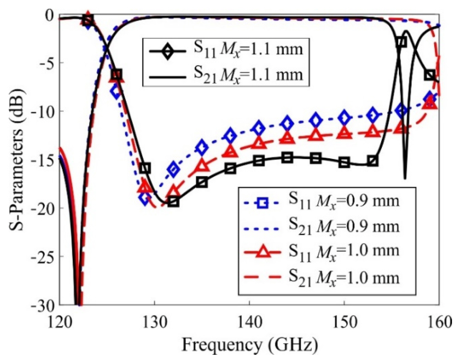
The simulated effects of changing the x-directed position of the matching via (Mx) on the reflection and transmission coefficients are depicted in Fig. 11. The figure shows that increasing the value of the Mx brings the upper resonance point closer to the lower one, and it also improves impedance matching. The final selected value of Mx was 1.1 mm due to the low values of the reflection coefficient at this value.
Fig. 12, by contrast, exhibits the simulated effect of varying the size of the inner parasitic patch lp on the reflection and transmission coefficients. By increasing lp, the capacitance between the edges of the patch and bottom metal, as well as with the top metal, increases; hence, it results in minimizing the values of the reflection coefficients. The optimized values of the design parameters are given in Table 1.
III. Experimental Validation
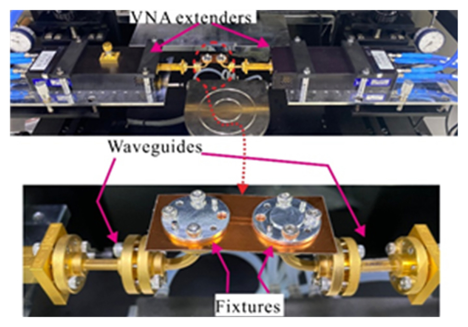
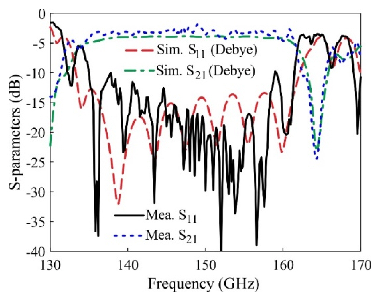
A photograph of the top and the bottom view of the fabricated back-to-back SIW transition is shown in Fig. 13. The total length of the back-to-back transition was LT = 2l + 23.5 mm. The S-parameter measurement setup consisted of PNA-X N5244B VNA with D-band VNA extenders, connecting WGs, and device under test (DUT), as shown in Fig. 14. SOLT calibration was performed up to the connecting WGs before measuring the DUT. A pair of circular fixtures was used to hold the PCB against the D-band WGs. A comparison of the simulated and measured S-parameters is depicted in Fig. 15. From the results, the back-to-back transition achieved a −10 dB IBW of 26.5 GHz (135–161.5 GHz) and a 3 dB BW of 28 GHz (133.8–161.8 GHz) in measurement compared to the simulated values of 26.8 GHz (127.2–154 GHz) and 28.5 GHz (126.7–155.2 GHz), respectively. To address the shift in the measurements, we modeled the frequency-dependent behavior of the dielectric constant using the Debye model using HFSS, as in one of the earlier studies [14], and the comparison of the results is plotted in Fig. 16. We observed that both results have reasonable agreement.
A comparison of the proposed transition with earlier works is shown in Table 2. In [9], a fin-line transition was proposed on a single substrate that obtains a −10 dB IBW of 40 GHz bandwidth in the D-band. However, the transition requires a large area and extra waveguide parts to measure the performance, which increases the overall cost. In [10] and [11], two W-band designs were presented using a double-layer PCB with respective −10 dB IBWs of 18.8 GHz and 20.7 GHz. The cost and complexity of a multi-layered design are higher than the proposed design. In [12], a rectangular SIW cavity with extra metal cladding was used to obtain a −10 dB IBW of 18 GHz, which is also not cost-effective. In [13], a wide-band single-layered based SIW transition was designed to offer a simulated −10 dB IBW of 30.3 GHz, but the measurement was done only for 18.2 GHz (48.8–67 GHz). Our work differs from [13] in terms of cavity used, detailed explanation of the modes used in the design, and measurement of the complete band, as in the simulation.
IV. Comparison
In this work, a WG-SIW transition is designed at the D-band for 6G communication. The TE320 mode of the SIW cavity was utilized in the design. By inserting a pair of vias in Trans-I, a TE320 mode-like distribution was generated at 142.8 GHz, which is the null-point frequency in the case of Trans-I. Finally, a parasitic patch was placed inside a coupling slot to improve impedance matching. The proposed transition was tested in a back-to-back configuration, and a −10 dB IBW of 26.5 GHz was achieved. In our future work, the proposed transition will be integrated with a D-band antenna for testing. The modeling of the frequency-dependent behavior of ɛr will also be considered for a closer prediction of the measurement results.