Design of S/X-Band Dual-Loop Shared-Aperture 2×2 Array Antenna
Article information
Abstract
This article proposes the S/X band dual-loop shared-aperture 2 × 2 array antenna, which is constructed using a unit-cell having one S-band element stacked on 3 × 3 X-band elements. The unit-cell employs a coupled-fed dual-loop structure with a direct-feed pin on the upper loop to obtain the broadband matching characteristics and low manufacturing error. This radar configuration has the advantages of easy installation and low cost. In addition, the thin loop structure of the upper layer S-band element is optimized so that the S-band element has electromagnetic (EM) transparent characteristics in the X-band. The extended via cavity wall is also applied outside the nine X-band elements to block the mutual coupling effect among the X-band elements. To confirm the feasibility of the proposed array antenna, the beamforming performance and active reflection coefficient (ARC) characteristics of the fabricated array are examined in the S/X band.
I. Introduction
In recent years, the demand for mounting S-band and X-band radars together on the same antenna aperture for military ship radar systems has been increasing [1, 2]. In such system configurations, the S-band radar is often used to search for targets, whereas the X-band radar is utilized to accurately track the detected targets [3, 4]. In general, because these multi-function radar (MFR) antennas are mounted separately to perform their individual functions, an increase in the radar cross section (RCS) of the system is unavoidable [5]. Separately mounted MFRs require more aperture area than conventional radar systems, making shared-aperture radar technologies increasingly attractive for such applications considering their manufacturability [6]. However, this shared-aperture configuration integrates multiple array elements in a limited space, which degrades the performance of the array antenna due to the electromagnetic (EM) coupling effects that arise from adjacent elements. To reduce this effect, various techniques have been introduced such as manipulating the orthogonal polarization properties, implementing meta-surfaces as isolators, and using shorting-pin structures [7, 8]. However, although these techniques can be applied in the same planar aperture, they are difficult to apply in the stacked shared aperture. To solve this problem in stacked shared-aperture antennas, various techniques have been reported. For example, the dual-mode stub-loaded resonator having second-order filtering characteristics was introduced to minimize the mutual coupling effect between the different band elements [9]. However, this antenna has a narrow matching bandwidth characteristic. In addition, a differential feeding method and perforated patch antenna for a shared-aperture antenna were proposed to achieve good isolation [10, 11]. However, these studies have the sub-array structure, which has a narrow scan range due to the grating lobe characteristic. Moreover, this structure cannot precisely adjust the phase of each element, and it is impossible to modularize the radar due to the asymmetric feeding structures. Thus, research from the perspective of the shared-aperture radar with an expandable full array including all S/X-band elements has not been fully conducted yet.
In this paper, we propose the S/X-band dual-loop shared-aperture 2 × 2 array antenna, which is constructed using a number of unit-cells as the basic elements. The proposed unit-cell comprises one S-band element being stacked on top of 3 × 3 X-band elements. Since the proposed array consists of the module-type symmetrical basic unit-cell, it is easy to expand to a full array having a large scale and is good for maintenance. In addition, the basic unit-cell includes overall configurations such as an S-band element, X-band elements, and simplified feeding networks, so that the unit-cell design can be directly applied to the full array. In order to obtain the broadband matching characteristics, a coupled-fed dual-loop structure is employed for the X- and S-band elements. Furthermore, to reduce manufacturing error, the feed pin is directly connected to the upper loop, where there is an optimized airgap between the S-band layer and the X-band layer. The unit-cell configuration has the advantages of easy installation and low cost because a damaged unit-cell can easily be replaced with an identical one. Since the X- and S-band elements should share a limited size aperture in a stacked configuration, the lower layer elements can be partially blocked by upper layer elements. To reduce these blockage effects, the thin loop structure of the upper layer S-band element is optimized so that the S-band element has EM transparent characteristics in the X-band. In addition, the extended via cavity wall is applied outside of the nine X-band elements to block the mutual coupling effect among the X-band elements. To verify the feasibility of the proposed antenna, the beamforming performance and the active reflection coefficient (ARC) characteristics of the fabricated 2 × 2 unit-cell array are investigated in the S/X-band.
II. Proposed Antenna Unit Cell Structure
Fig. 1 shows the conceptual diagram for a modularized shared-aperture radar. The basic unit-cell contains stacked-type multi-band layers (S-band and X-band), which have a shared-aperture configuration for easy installation. The designed unit-cells are repeatedly assembled and expanded to form a full array module, which becomes the array antenna component of the MFR. This radar configuration has the advantages of enabling simple system expansion and maintenance because a damaged cell can be easily replaced with an identical one. In addition, since identical unit-cells are repeatedly used, massive-scale production is possible at low manufacturing cost.
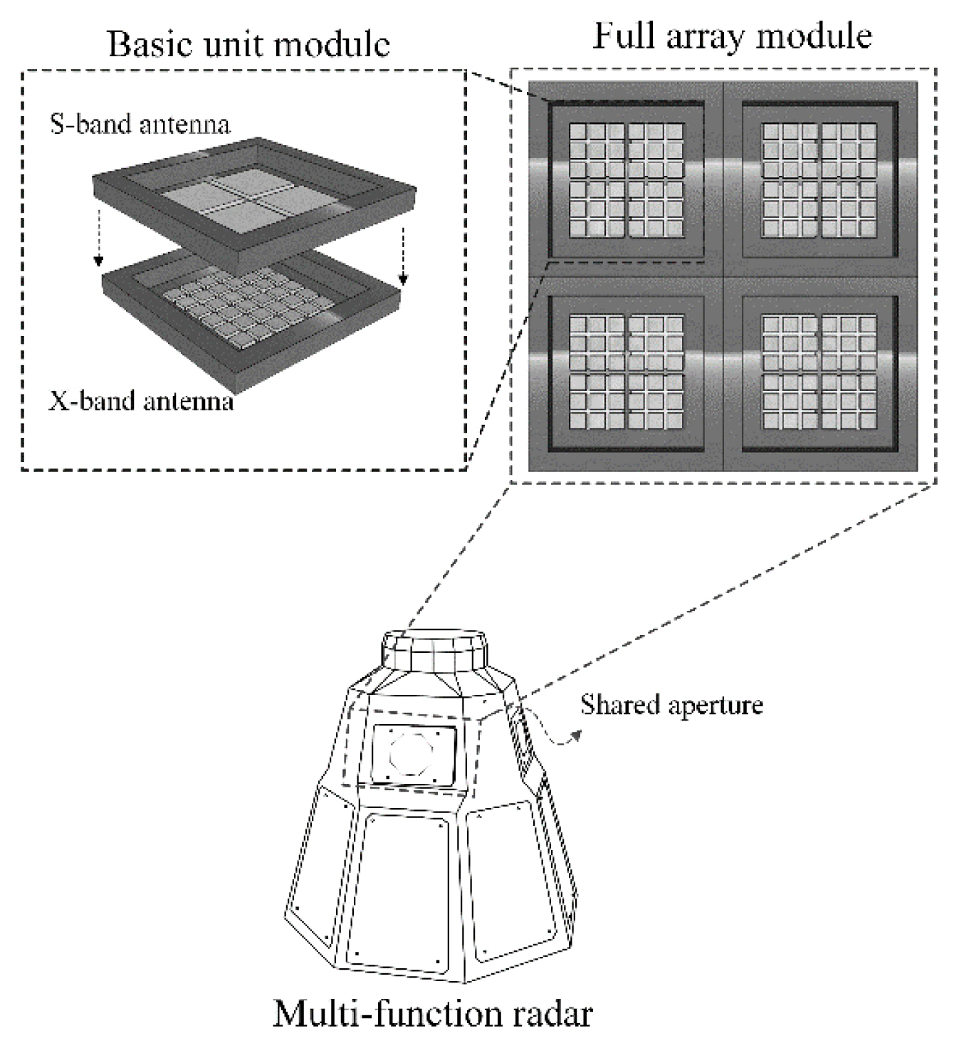
A conceptual diagram for the modularization of a shared-aperture antenna using a unit-cell.
Fig. 2 illustrates the configuration of the proposed unit-cell, which consists of one S-band element and 3 × 3 X-band elements. To obtain the broadband matching characteristics, the coupled-fed dual-loop structure is employed for the X-band and S-band elements. The two layers of the S-band element are stacked on top of the two layers of the X-band elements, as shown in Fig. 2(a). An optimized airgap is present between the S-band layer and the X-band layer to reduce the manufacturing error for soldering. In general, soldering in stacked layers leads to an unavoidable space; however, the radiation element layer that is connected to the feed pin must be soldered. Therefore, the feed pin is directly connected to the upper loop for minimum manufacturing error, where the optimized airgap is present. On the other hand, since the X- and S-band elements should share a limited-sized aperture in a stacked configuration, the lower layer X-band elements may be partially blocked by the upper layer S-band elements. To reduce such EM blocking effects, the thin loop structures of the upper layer S-band element are optimized so that the S-band element has EM transparent characteristics in the X-band, which implies that the S-band element on top does not affect the X-band element operation. The top view of the optimized S/X-band element is shown in Fig. 2(b). The optimized thicknesses of the loop are ts1, ts2, tx1, and tx2 for the first and second S-band and X-band layers, respectively. The outer edge lengths of the loop are ls1, ls2, lx1, and lx2, and the outer edge widths of the loop are ws1, ws2, wx1, and wx2 for the first and second S-band and X-band layers, respectively. To block the mutual coupling effect among X-band elements, an extended via cavity structure is used instead of a normal cavity wall outside of the nine X-band elements for stable manufacturing. The heights of the first and second S-band and X-band layers are hs1, hs2, hx1, and hx2, respectively. The proposed antenna is made of TLY-50 substrates (ɛr = 2.2, tan δ = 0.0009). The detailed geometrical parameters are derived using the FEKO electromagnetic simulator [12] and are listed in Table 1.
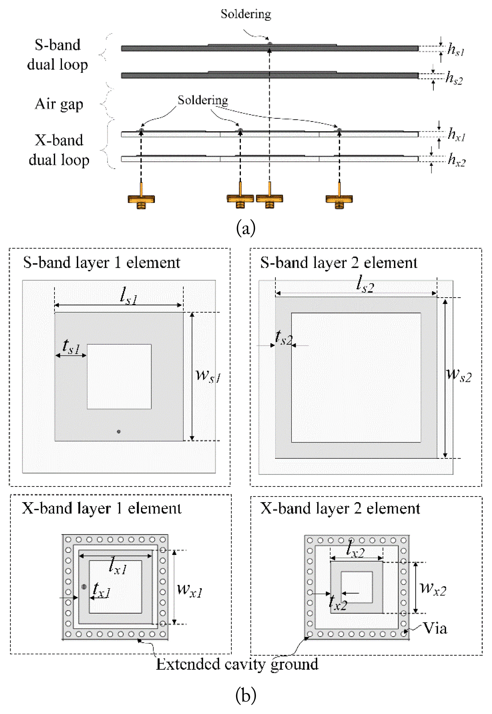
Configuration of the proposed unit-cell: (a) side view and (b) top view of the S/X-band element.
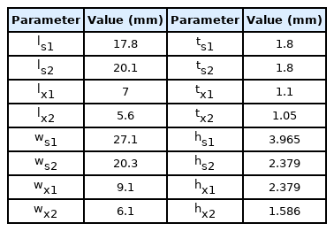
Geometrical parameters of the proposed antenna
Fig. 3 shows the average gain and reflection coefficient performance of the S/X-band element according to the thickness of S-band loop (Lsw) in the unit-cell. The average gain of the central X-band element is between 9.5 GHz and 10.5 GHz, and the average reflection coefficient of S-band loop is between 2.9 GHz and 3.2 GHz. The average gain of the X-band central element decreases as the Lsw increases, as shown in Fig. 3. Since an increase in thickness of the S-band loop, Lsw, leads to an increase of the blockage area for the central X-band element, the lower layer central X-band element may be affected. To reduce these EM blockage effects, the thin loop structures of the upper layer’s S-band element should be optimized so that the S-band element has minimum reflection coefficient and EM transparent characteristics for the X-band elements in the under-layer. At the optimum Lsw of 1.8 mm, the maximum average boresight gain of 5.29 dBi for the X-band center element and a minimum average reflection coefficient of −13.9 dB in the S-band are achieved.

Average gain and reflection coefficient of the S/X-band element according to the thickness of the S-band loop.
Fig. 4 presents the reflection coefficients and boresight gains of the S-band and X-band elements. The reflection coefficient of the S-band element has a bandwidth of 328 MHz (2.89 GHz to 3.22 GHz, |Γ| < −10 dB), for which the fractional bandwidth is greater than 10.8%. The boresight gain is maintained above 3 dBi in the operating bandwidth, as shown in Fig 4(a). Among the X-band elements, the bandwidth of the central element is 1.4 GHz (9.17 GHz to 10.57 GHz, |Γ| < −10 dB), for which the fractional bandwidth is greater than 14.3%. Moreover, the boresight gain is maintained above 4.5 dBi in the operating bandwidth, as shown in Fig 4(b).
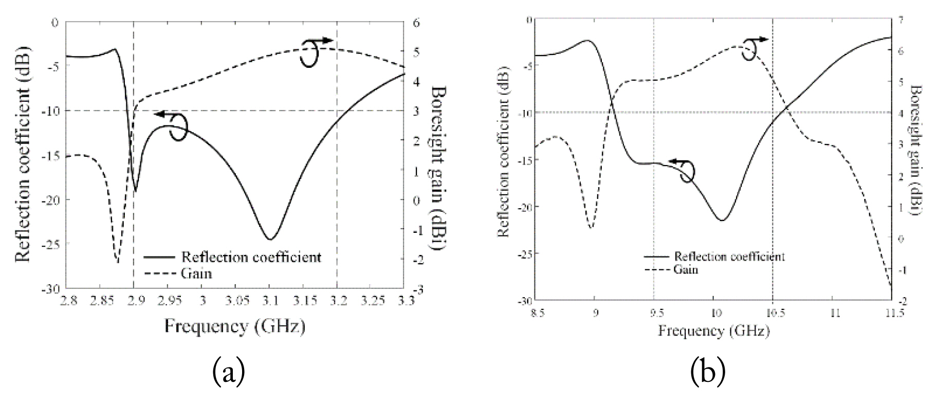
Reflection coefficient and boresight gain of the proposed unit-cell: (a) S-band and (b) X-band.
III. Verification of the Proposed Antenna Array
To verify the feasibility of the proposed antenna, a 2 × 2 unit-cell array is fabricated and measured in a full anechoic chamber. Fig. 5 shows the top and side views of the fabricated 2 × 2 unit-cell array. The two S-band and X-band layers are combined using dielectric bolts, and each part is assembled on a metallic cage body. In the array configuration, the four identical unit-cells are separated from adjacent elements by a distance of Ds (51 mm), and the 36 elements of the X-band array, for which feed-to-feed distance is Dx (17 mm), are stacked under the S-band elements as shown in Fig. 5.
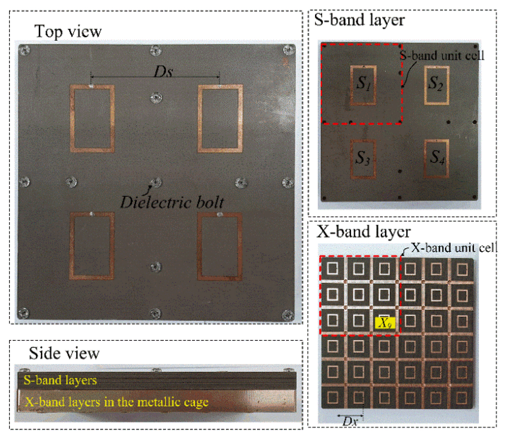
Configuration of the fabricated 2 × 2 unit-cell array.
Fig. 6 shows the measurement setup in the full anechoic chamber. The test probe antennas in the yellow rectangle are placed around the antenna under test (AUT) in the red rectangle, where the proposed unit-cell array is fixed with the zig. The reflection and active element patterns for the 40 ports were fully measured in the S/X band. Fig. 7 shows the reflection coefficient of the fabricated 2 × 2 unit-cell array for the first S-band element (S1) and central X-band element (X9). The solid, dotted, and dashed lines indicate the measured reflection coefficient, ARC, and simulated reflection coefficient, respectively. The ARC observed at an element m with the fully excited array for the θ0 steering is calculated as follows [13]:
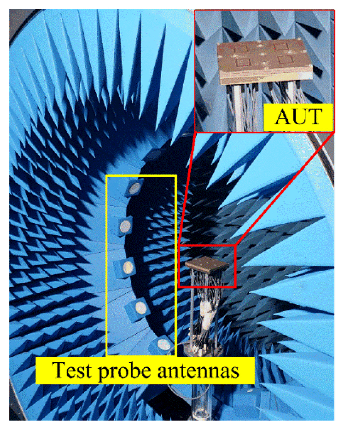
Measurement setup in the full anechoic chamber.
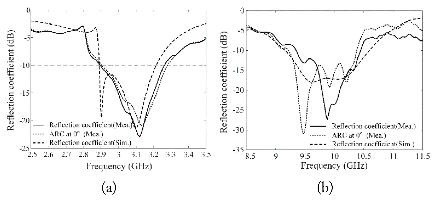
Reflection coefficient and the active reflection coefficient (ARC) of the fabricated 2 × 2 unit-cell array: (a) S-band (S1) and (b) X-band (X9).
where u0 is kd sinθ0 and d is the array distance. The reflection coefficient of S1 has a bandwidth of 390 MHz (2.83 GHz to 3.32 GHz, |Γ| < −10 dB), and the measured results are in good agreement with the simulated ones, as shown in Fig. 7(a). The measured values of the ARC for 0° steering are almost similar to the passive reflection coefficient value. Further, Fig. 7(b) shows the reflection coefficient characteristics of X9. The bandwidth is 1.1 GHz (9.3 GHz to 10.4 GHz, |Γ| < −10 dB), for which the fractional bandwidth is greater than 12.2%, and the bandwidth of the ARC for 0° steering is similar to that of the passive reflection coefficient.
Fig. 8 illustrates the ARC in the UV domain [14, 15], when the steering weighting vectors are applied to each element of the array. The dashed black line represents the 30° azimuth over elevation steering angle region. The color shows the ARC level in dB scale, where the darker blue indicates better matching characteristics. The peak ARCs in the 30° azimuth over elevation steering angle region are −11 dB and −6 dB for S1 and X9, respectively, as shown in Fig. 8(a) and Fig. 8(b).

ARC in the UV domain: (a) at 3 GHz (for S1) and (b) at 10 GHz (for X9).
Fig. 9 shows the array beam pattern for the 2 × 2 unit-cell array. The boresight gains at 3 GHz for the simulated 0° steering beam pattern and measured 0°, 10°, and 20° steering patterns are 9 dBi, 9.4 dBi, 9.4 dBi, and 9.1 dBi, respectively. The measured and simulated results are in good agreement, as shown in Fig. 9(a). The boresight gains at 10 GHz for the simulated 0° steering beam pattern and measured 0°, 10°, and 20° steering patterns are 19.4 dBi, 18.4 dBi, 18 dBi, and 17.7 dBi, respectively, as shown in Fig. 9(b).
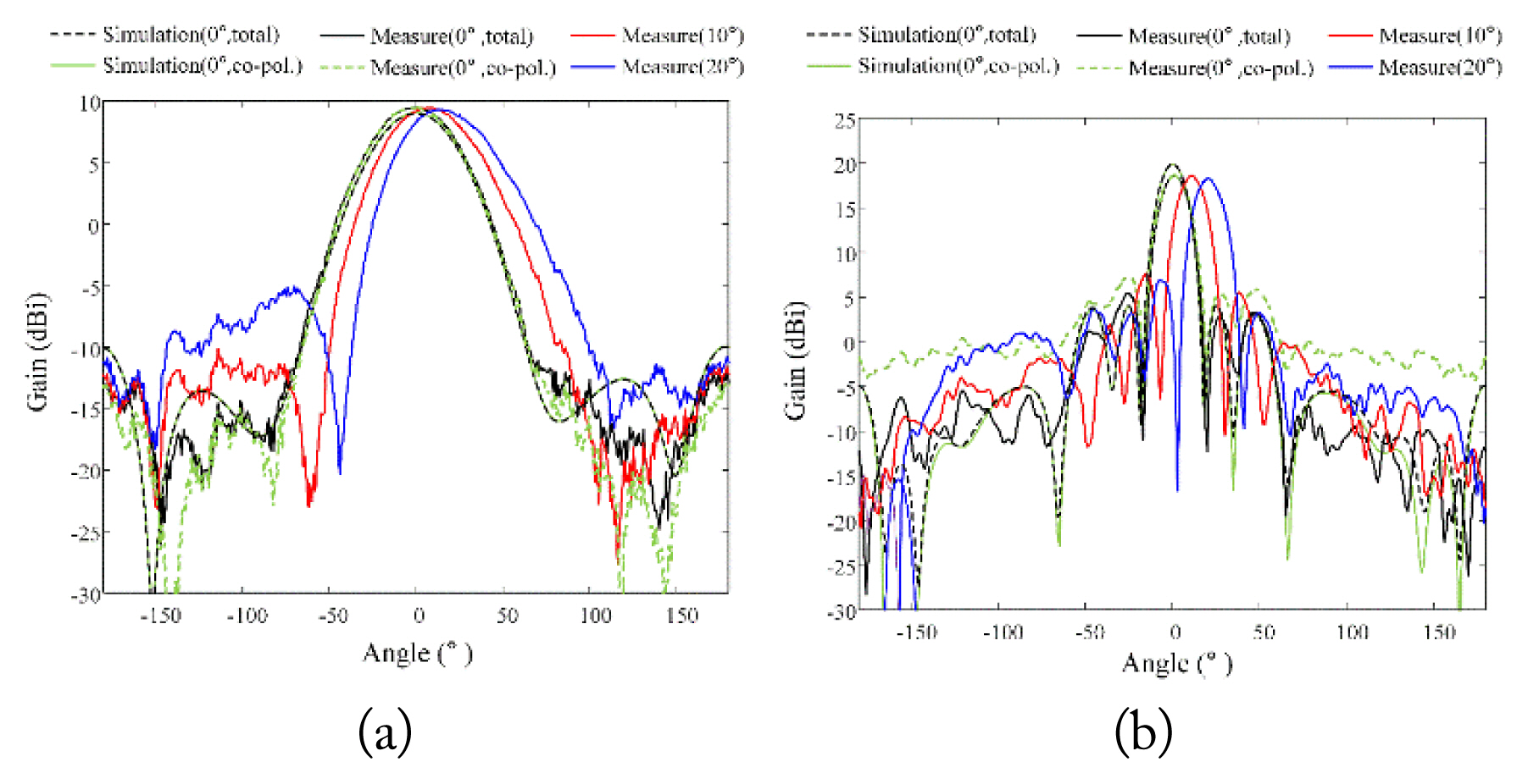
Array beam pattern for the 2 × 2 unit-cell array: (a) at 3 GHz and (b) at 10 GHz.
The basic unit-cell of the proposed array includes overall configurations such as an S-band element, X-band elements, and simplified feeding networks, so that the unit-cell design can be directly applied to the full array, where each element has equal phase delay. The full array can be various shapes because the proposed array consists of the modularized symmetrical basic unit-cell. Fig. 10 illustrates the 12 × 12 full-scale unit-cell array configuration with its expected radiation pattern, where the dimension L is 204 mm. The 12 × 12 array configuration can be obtained by extending the 2 × 2 array because the proposed array consists of the modularized basic unit-cells having symmetrical structure, as shown in Fig. 10(a). Fig. 10(b) shows the expected radiation pattern of the full array, where the black and red solid lines indicate the X-band beam pattern and the S-band beam pattern, respectively. The boresight gains are 36.1 dBi and 26.9 dBi, respectively.
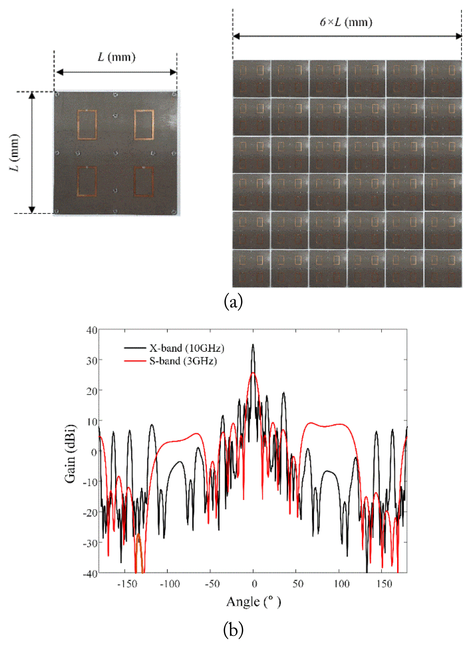
A 12 × 12 full-scale unit-cell array: (a) configuration and (b) radiation pattern.
IV. Conclusion
We investigated the S/X-band dual-loop shared-aperture 2 × 2 array antenna, which consisted of 2 × 2 S-band and 6 × 6 X-band stacked dual-loops with a recursive coupled-fed structure to obtain the broadband matching characteristics. Moreover, we employed the upper loop direct feed structure for manufacturing tolerance. In addition, an extended via cavity structure and optimized S-band element with EM transparent characteristics were applied to reduce the coupling effects. To confirm the feasibility of the proposed 2 × 2 unit-cell array, the beamforming performance and ARC characteristics of the fabricated array were investigated in the S/X-band.
The peak ARC in the 30° azimuth over elevation steering angle region were −11 dB and −6 dB for S1 and X9, respectively, and the maximum gains at 3 GHz and 10 GHz for the 0° steering were 9.4 dBi and 18.4 dBi, respectively.
Acknowledgments
This research has been supported by the Defense Challengeable Future Technology Program of the Agency for Defense Development, Republic of Korea.
References
Biography

Sungsik Wang received his B.S. and M.S. degrees in radio science and engineering from Hanyang University, Seoul, Korea in 1997 and 1999, respectively, and a Ph.D. in the department of Electronic & Electrical Engineering from Hongik University, Seoul, Korea in 2021. In September 2021, he joined the Department of Electrical, Electronic, & Communication Engineering, Hanyang Cyber University, Seoul, Korea, where he is currently an assistant professor. His research interests include beam propagation under abnormal atmospheric phenomena, broadband antenna design, use of the optimization algorithm in developing antennas, and antenna array beamforming.

Doyoung Jang received his B.S. degree in information and telecommunication engineering from Dongyang Mirae University, Seoul, Republic of Korea in 2018 and an M.S. in the Department of Electronic & Electrical Engineering from Hongik University, Seoul, Korea in 2020. He worked as a research engineer in MOASOFT, Seoul, Korea from 2015 to 2018. He is currently working toward his Ph.D. in electronics and computer engineering at Hongik University, Seoul, Korea. His research interests include direction finding, passive radars, electromagnetic wave propagation, and electromagnetic environmental effects.

Youngwan Kim received his B.S and M.S. degrees in radio engineering from Kwangwoon University, Seoul, Korea in 2005 and 2007, respectively. He has been a chief research engineer with LIG Nex1, where he has been involved in the development of antennas for radar systems. His research interests include array antennas and meta material.

Hosung Choo received his B.S. degree in radio science and engineering from Hanyang University in Seoul in 1998, and his M.S. degree and Ph.D. in electrical and computer engineering from the University of Texas at Austin in 2000 and 2003, respectively. In September 2003, he joined the School of Electronic and Electrical Engineering, Hongik University, Seoul, Korea, where he is currently a full-time professor. His principal areas of research are the use of the optimization algorithm in developing antennas and microwave absorbers. His studies include the design of small antennas for wireless communications, reader and tag antennas for RFID, and on-glass and conformal antennas for vehicles and aircraft.