Analysis Method for a Multi-Section Rat-Race Hybrid Coupler Using Microstrip Lines
Article information
Abstract
An analysis method for a multi-section rat-race hybrid coupler with a large bandwidth is presented. The proposed coupler has only a few additional microstrip lines compared to a single-section coupler. A complete analysis method is derived and validated through even- and odd-mode analysis, considering the asymmetric structure of the proposed coupler. To demonstrate the effectiveness of the design, two two-section rat-race couplers with an operating frequency of 2 GHz and splitting ratios of 1:1 and 1:2 were simulated and fabricated. Measurements of the fabricated couplers yielded results in good agreement with the simulation results, demonstrating wide bandwidth characteristics.
I. Introduction
The single-section rat-race coupler is a key passive component in RF/microwave circuits. Its important feature is that it has the ability to split the signal, providing power when inphase and out-of-phase. The in-phase division operates like a Wilkinson divider, and when an out-of-phase signal is divided, it can be used for balanced amplifiers, balanced mixers, and antenna feed networks [1–3]. However, conventional rat-race couplers are large and have narrow band characteristics.
Many researchers have studied various methods to overcome these shortcomings. For example, a combination of microstripslot transitions and a three-line parallel-coupled microstrip structure [4], the addition of a fifth port to the conventional four-port design [5], a cascadable hybrid-ring coupler [6], broadside-coupled asymmetric coplanar striplines [7], a novel coplanar waveguide phase inverter [8], a vertically installed planar coupler [9], and a unit element at each port and ideal phase inverter at one of the ring arms [10] have all been used to increase the bandwidth significantly. However, because these methods use air bridges, narrow slots in the ground, or narrow transmission lines, the rat-race hybrid coupler does not have sufficient power capacity. Furthermore, some of these methods have complex structures, are expensive to manufacture, and are not suitable for microstrip circuits.
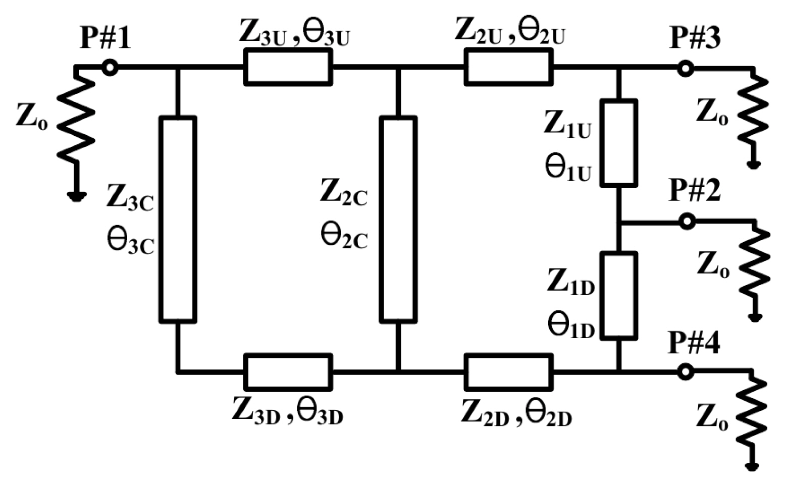
In this paper, we propose a multi-section wideband rat-race coupler consisting of only microstrip lines. In this structure, the λ/4 and λ/2 transmission lines that constitute a rat-race coupler are connected in series and in parallel. The proposed coupler structure is shown in Fig. 1. This structure is presented in [11], and no interpretation method for it is presented. Here, we introduce the interpretation method through even- and odd-mode analysis. Such a multi-stage rat-race coupler can increase the bandwidth to more than 50% from the 20% bandwidth of a single structure. The proposed coupler analysis method is confirmed through theory, simulation, and measurement.
II. Theory
Fig. 1 shows the structure of our multi-stage rat-race coupler. It consists of transmission lines of two types with electrical lengths of θ1U, θ2U, θ3U, θ1D, θ2D, θ3D, θ2C, and θ3C. The impedance of port #1 to #4 is Zo = 50 Ω.
The proposed rat-race coupler is analyzed using even- and odd-mode analysis methods; Fig. 2(a) and 2(b) show the even- and odd-mode equivalent circuits, respectively. In the even mode, the voltage at ports #3 and #4 of the structure of Fig. 1 should have equal amplitude and be in phase. In this case, port #2 is virtually open circuit. Thus, the equivalent circuit for the even-mode excitation is shown in Fig. 2(a). In addition, in the odd mode, the voltage at ports #3 and #4 of the structure of Fig. 1 should have equal amplitude and be out of phase. In this case, port #2 is virtually short circuit. Thus, the equivalent circuit for the odd-mode excitation is shown in Fig. 2(b).
The S-parameters of the proposed coupler can be calculated from the even- and odd-mode reflection and transmission coefficients of the two ports (port #3 and port #4), which are excited by the even- and odd-mode excitation according to the following equations:
where, respectively, Γ33o, Γ 33e are the reflection coefficients at port #3 for odd- and even-modes; Γ44o, Γ44e are the reflection coefficients at port #4 for odd- and even-modes; T31o, T31e are the transmission coefficients from port #1 to port #3 for odd- and even-modes; T41o, T41e are the transmission coefficients from port #1 to port #4 for odd- and even-modes; T34o(=T43o), T34e(=T43e) are the transmission coefficients from port #4 to port #3; and vice versa for odd- and even-modes.
In addition, in the equivalent circuit of Fig. 2, port #2 operates as open or short, so the S-parameters between port #1 and #2 are as follows.
1. Calculation of Γ33o, Γ33e, T31o, and T31e
In this case, port #4 is terminated with a matched load. The equivalent ABCD matrix is the product of the cascaded matrices representing different circuit elements connected between ports #1 and #3, including the effect of terminated port #4.
Even mode
In Fig. 2(a), the impedance values of ZXe and ZYe are as follows:
In addition, the ABCD matrices of the circuit composed of the Z2C – ZYe – Z3D – Z3C and Z3U networks are as follows:
Because the circuits shown in Eqs. (13) and (14) are connected in parallel, it is necessary to convert these equations into admittance matrices. After adding the transformed admittance matrix, we transform back to the ABCD matrix (A11t/B11t/C11t/D11t). Finally, after obtaining the ABCD matrix from port #3 to port #1, the reflection and transmission coefficients can be calculated as follows:
Odd mode
In Fig. 2(b), the impedance values of ZXo and ZYo are as follows:
In addition, the ABCD matrices of the circuit composed of the Z2C - ZYo - Z3D - Z3C and Z3U networks are as follows:
Because the circuits expressed by Eqs. (14) and (21) are connected in parallel, it is necessary to convert these equations into admittance matrices. After adding the transformed admittance matrix, we transform back to the ABCD matrix (A22t/B22t/C22t/D22t). Finally, after obtaining the ABCD matrix from port #3 to port #1, the reflection and transmission coefficients can be calculated as follows:
2. Calculation of Γ4o, Γ4e, T41o, and T41e
In this case, port #3 is terminated with a matched load. The equivalent ABCD matrix is the product of the cascaded matrices representing different circuit elements connected between ports #1 and #4, including the effect of terminated port #3.
Even mode
In Fig. 2(a), the impedance values of ZNe and ZMe are as follows:
Furthermore, the ABCD matrices of the circuit composed of the Z2C - ZMe - Z3U and Z3D - Z3C networks are as follows:
Because the networks expressed by Eqs. (27) and (28) are connected in parallel, it is necessary to convert these equations into admittance matrices. After adding the transformed admittance matrix, we transform back to the ABCD matrix (A33t/B33t/C33t/D33t). Finally, after obtaining the ABCD matrix from port #4 to port #1, the reflection and transmission coefficients can be calculated as follows:
Odd mode
In Fig. 2(b), the impedance values of ZNo and ZMo are as follows:
In addition, the ABCD matrices of the circuit composed of the Z2C - ZMo - Z3U and Z3D - Z3C networks are as follows:
Because the circuits of Eqs. (35) and (36) are connected in parallel, it is necessary to convert these equations into admittance matrices. After adding the transformed admittance matrix, we transform back to the ABCD matrix (A44t/B44t/C44t/D44t). Finally, after obtaining the ABCD matrix from port #4 to port #1, the reflection and transmission coefficients can be calculated as follows:
3. Calculation of T34e(=T43e) and T34o(=T43o)
In this case, port #1 is terminated with a matched load. The equivalent ABCD matrix is the product of the cascaded matrices representing different circuit elements connected between ports #3 and #4, including the effect of terminated port #1.
Even mode
In Fig. 2(a), when Port #1 is terminated, the ABCD matrices of the circuit composed of the Z3U – ZO – Z3C – Z3D and Z2C networks are as follows:
Because the circuits of Eqs. (9) and (41) are connected in parallel, it is necessary to convert these equations into admittance matrices. After adding the transformed admittance matrix, we transform back to the ABCD matrix (A55t/B55t/C55t/D55t). Finally, after obtaining the ABCD matrix from port #3 to port #4, the reflection and transmission coefficients can be calculated as follows:
Odd mode
In Fig. 2(b), when port #1 is terminated, the ABCD matrices of the circuit composed of the Z3U – ZO – Z3C – Z3D and Z2C networks have the same values as in the even mode. Finally, the ABCD matrix from port #3 to port #4 is calculated as follows:
The impedances of the microstrip lines that can be implemented were set to 0.5Zo ≤ ZiD, ZiU, ZiC ≤ 2Zo i = 1, 2, 3, and the electrical lengths were set to θ1U = θ2U = θ3U = θ1D = θ2D = θ3D = 90° and θ2C = θ3C = 180°. In addition, the S-parameters of the two-stage rat-race coupler were obtained under the following conditions:
Reflection characteristics:
Coupling characteristics:
where k2 is the power dividing ratio.
Isolation characteristics:
The impedance values of the transmission line that satisfy the S-parameters of the multi-section coupler are determined by using the reflection and transmission coefficient equations through even- and odd-mode analysis. They were obtained while changing the eight impedance values constituting the ratrace coupler under the previously set condition using MATLAB. Since the obtained impedance value satisfies the design condition at a specific frequency, and from these values, the impedance value that satisfied the broadband bandwidth condition was selected.
III. Simulation and Experimental Results
To confirm the validity of the analysis method, we fabricated two-stage rat-race couplers with 1:1 and 1:2 splitting ratios at an operating frequency of 2.0 GHz. These were implemented on the substrate of an FR-4 printed circuit board with dielectric constant ɛr = 4.4, dielectric thickness h = 0.787 mm, and copper thickness t = 0.035 mm. The simulation was performed using Microwave Office software, version 13, developed by Cadence. The configuration process for the two-stage rat-race coupler with a 1:1 splitting ratio was as follows.
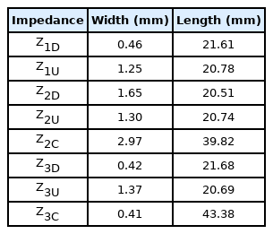
The electrical lengths of each transmission line and the impedance values of the transmission line constituting the coupler were calculated using the equations obtained in Section II. In k2 = 1 condition, the dimensions are listed in Table 1. The parameters for designing a two-stage rat-race coupler with a 1:2 splitting ratio were obtained using the same method, and the related information is summarized in Table 2.
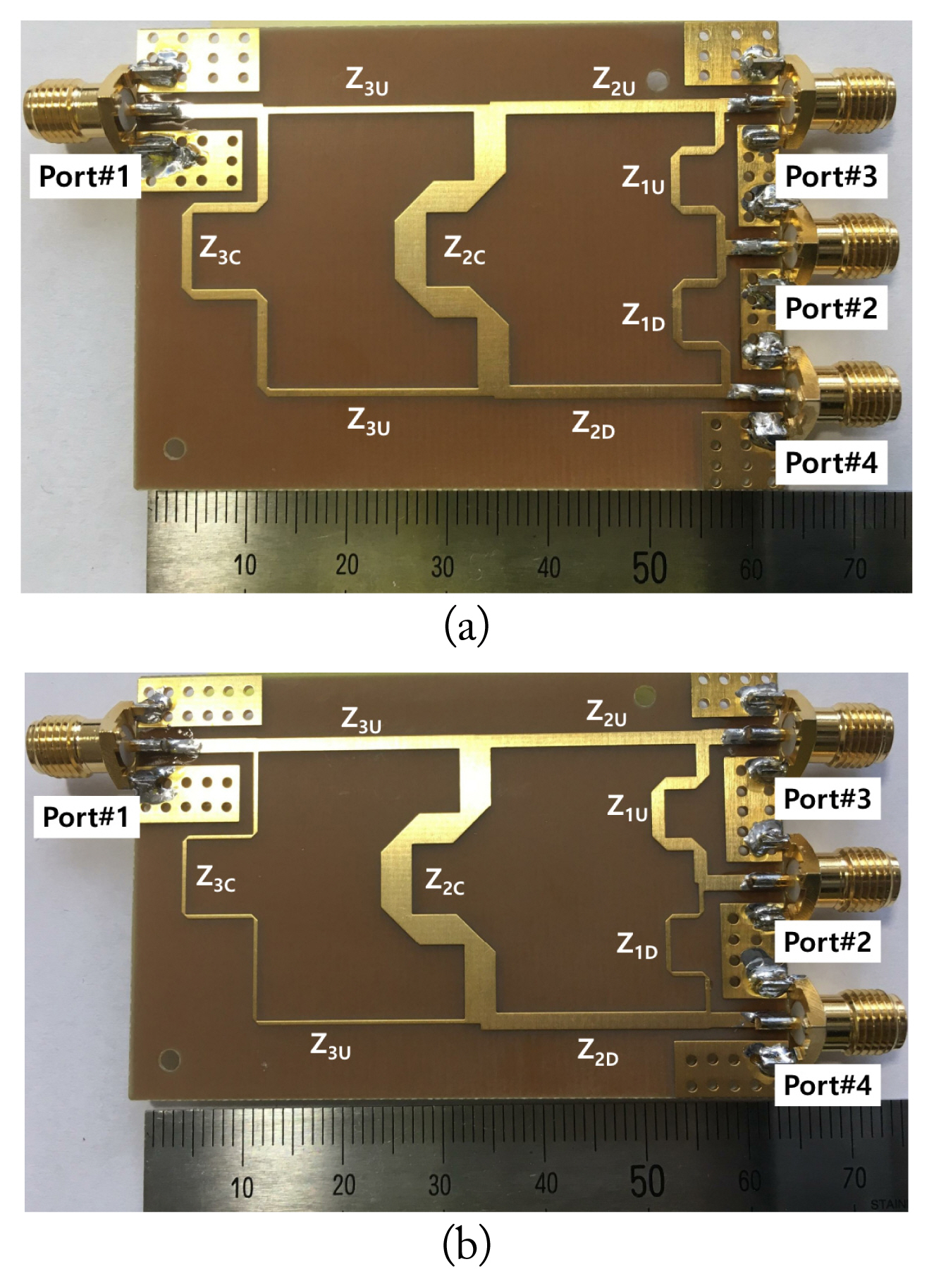
Fig. 3(a) and 3(b) show photographs of the two-stage ratrace couplers with 1:1 and 1:2 splitting ratios. In the photographs, the implemented impedance values of each transmission line of each coupler are the result of an optimization process for electrical properties.
Fig. 4(a)–4(c) show the measured and simulated S-parameters, respectively, of the proposed coupler with a 1:1 power ratio. The figures show insertion losses of |S31| = −3.93 dB, |S41| = −3.80 dB, |S32| = −3.33 dB, and |S42| = −3.45 dB. The isolation of |S21| and |S43| was greater than 25 dB.

Measured and simulated S-parameters of the proposed coupler with a 1:1 splitting ratio: (a) |S11|, |S31|, |S41|, (b) |S32|, |S42|, |S22|, and (c) |S21|, |S43|, |S33|, |S44|.
The input return losses of |S11| and |S22| were better than −15 dB, and the output return losses of |S33| and |S44| were better than −15 dB at the center frequency of 2.0 GHz. The measured −15 dB bandwidths of return losses of |S11|, |S22|, |S33|, and |S44| were 1.57–2.62 GHz, 1.54–2.60 GHz, 1.30–2.72 GHz, and 1.50–2.71 GHz, with fractional bandwidths of 52.5%, 53.0%, 71.0%, and 60.5%, respectively; for isolation |S21|, |S43| the bandwidths were 1.49–2.85 GHz and 1.58–2.60 GHz with fractional bandwidths of 68.0% and 51.0%, respectively.
Fig. 5(a)–5(c) show the measured and simulated S-parameters of the proposed coupler with a 1:2 power ratio. The figures show insertion losses of |S31| = −5.38 dB, |S41| = −2.66 dB and |S32| = −2.21 dB, |S42| = −5.05 dB, and isolations of |S21| and |S43| greater than 20 dB. The input return losses of |S11| and |S22| were better than −15 dB, and the output return losses of |S33| and |S44| were better than −15 dB at the center frequency of 2.0 GHz. The measured −15 dB bandwidths of |S11|, |S22|, |S33|, and |S44| were 1.41–2.73 GHz, 1.62–2.52 GHz, 1.59–2.60 GHz, and 1.49–2.68 GHz, with fractional bandwidths of 66.0%, 45.0%, 50.5%, and 59.5%, respectively; for the isolations of |S21| and |S43|, the bandwidths were 1.48–2.89 GHz and 1.53–2.62 GHz, with fractional bandwidths of 70.5% and 54.5%, respectively. Fig. 6 shows that the amplitude and phase imbalances between the output ports in the two-stage coupler were ±0.5 dB in the 1.58–2.72 GHz range and ±5° in the 1.64–2.65 GHz range, respectively. Table 3 shows a comparison of our rat-race coupler with a conventional multi-section coupler.

Measured and simulated S-parameters of the proposed coupler with a 1:2 splitting ratio: (a) |S11|, |S31|, |S41|, (b) |S32|, |S42|, |S22|, and (c) |S21|, |S43|, |S33|, |S44|.

Imbalance of amplitude and phase between the output ports of the proposed coupler with a 1:1 splitting ratio.
IV. Conclusion
An analysis method for a two-stage rat-race coupler with a planar structure and wideband performance has been presented. The proposed device uses only microstrip lines and has the feature of being convenient to implement. Our measurements show more than 25 dB of isolation between ports #1 and #2 across 70% fractional bandwidth, and between ports #3 and #4 across 50% fractional bandwidth. Our device has more than 15 dB return loss across 50% fractional bandwidth, and ±2.5° phase deviation across the 1.64–2.65 GHz band.
References
Biography

Young Kim received his B.S., M.S., and Ph.D. in electronics engineering from Sogang University, Seoul, South Korea in 1986, 1988, and 2002, respectively. He developed cellular and PCS linear power amplifiers at Samsung Electronics Co. Ltd. In 2003, he joined the School of Electronics Engineering, Kumoh National Institute of Technology, Gumi, South Korea, where he is currently a professor. His areas of interest are the design of high-power amplifiers and linearization techniques, and RF and microwave circuit analysis and design.


