


I. Introduction
Due to speedy developments in modern communication, there is a pressing need for reconfigurable antennas. Decades ago, individual antennas were employed to obtain different operating frequencies, increasing the dimensions of the system. Conversely, UWB antennas can be utilized to attain a wide frequency range (3.1ŌĆō10.6 GHz) [1]. However, there are some disadvantages in using UWB antennas, such as interference and co-existence with other radios. Thus, the concept of reconfigurability has evolved to avoid these scenarios. Frequency reconfigurability [2] has significantly reduced the antenna size, so that they can easily be employed in any compact handheld device. There are two other categories of reconfigurable antennas: polarization [3] and pattern [4]. It is possible to realize two or more reconfigurabilities at the same time depending on the number of switches. The cognitive radio system represents the near future of wireless communication, in which an antenna tunes to the desired frequency based on the available spectrum [5]. Accordingly, reconfigurable antennas are one of the best solutions for such adaptive systems and are used in satellite communications and radar systems.
Generally, reconfigurability is attained by using various switching devices, such as PIN diodes [6], varactor diodes [7], microelectromechanical systems (MEMS) switches [8], lumped elements [9], or optical switches [10]. These devices alter the structure (length) of the radiating element depending on the ON and OFF conditions. In the literature, many reconfigurable antennas have been designed that incorporate frequency, polarization, pattern, and hybrid reconfigurability (depending on the application). In [11], a PIN diode was included in the center of the slot, and frequency diversity was obtained by changing the bias voltage and keeping the other parameters (such as geometry and feeding probe) constant. The bandwidth can also be changed by varying the PIN diode. In [12], a ground plane was embedded with a DGS structure having two symmetrical U-shaped slots (with open ends) and an I-shaped slot (with a short end). The ground plane incorporated three PIN diodes to achieve multiband resonances.
In [13], a frequency reconfigurable antenna with coplanar waveguide (CPW) feeding was designed to cover a wide frequency range (2ŌĆō10 GHz). The antenna used four PIN diodes to achieve different resonant frequencies in the wide frequency band. Further, the type of feeding, structure of the radiator, and number of diodes employed were the deciding factors for the operating frequency ranges. Discussions about a reconfigurable antenna having proximity couple feeding for WLAN and sub-6 GHz applications were presented in [14]. The antenna consisted of two substrates (separated by air) with four PIN diodes. However, the dimensions of the antenna are large and the structure is complex with this type of feeding. Finally, by using a reconfigurable feed network, frequency and polarization diversity can be achieved [15]. From the literature, it can be understood that PIN diodes are more user friendly in terms of less switching complexity, higher speed and reliability.
A compact, low-profile, frequency-reconfigurable microstrip patch antenna built on a FR4 substrate is discussed in this paper. Compared to conventional reconfigurable antenna models, this antenna only contains one PIN diode and generates five resonant frequencies. During forward bias, the operating bands are 2.4 and 5.3 GHz, whereas they are 3.3 and 5.9 GHz in reverse bias. These operating frequencies cover the WLAN (2.4 and 5.9 GHz) and 5G (5.3 and 3.7 GHz) bands. During zero bias, the antenna operates between 3.6 and 4.8 GHz.
Section II presents a discussion about the antenna design, including the geometry, design equations, switching techniques, and current distribution. Section III focuses on the simulation and fabrication results, while Section IV provides a brief conclusion of the proposed work.
II. Antenna Design
1. Geometry of the Proposed Antenna
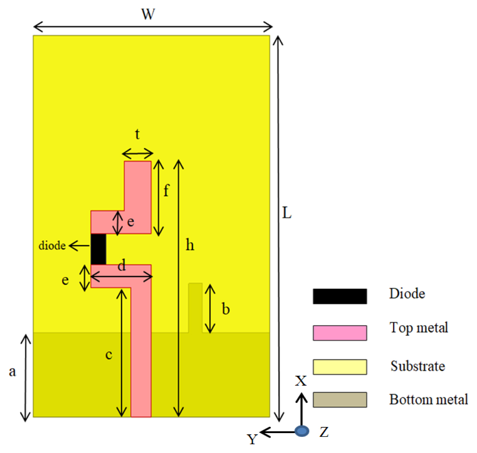
The model consists of two asymmetric L-shaped rectangular patches, with one of the patches fed through a 50 ╬® microstrip line. The antenna was printed on a lossy FR4 substrate material ŌĆörelative permittivity (╔ør) of 4.4 and tangent loss (╬┤) of 0.02ŌĆö with a thickness of 1.6 mm. The use of FR4 was preferred in the proposed model because of its affordability and availability. The radiating element was backed by a metallic truncated ground plane to provide optimum efficiency, gain, and directivity. A rectangular stub was placed on the ground to improve impedance matching at higher resonant frequencies. An electrical path was provided between the two rectangular patches through a PIN diode. A full wave electromagnetic (EM) simulatorŌĆöAnsys High Frequency Structure Simulator (HFSS)ŌĆöwas used to carry simulation of the proposed design. The total length of the radiator was 33.5 mm, and the width was 4 mm, and the overall dimensions was 40 mm ├Ś35 mm ├Ś1.6 mm. The geometry of the antenna is shown in Fig. 1. Table 1 presents the dimensions of the proposed model.
2. Design Equations
The effective length and dielectric permittivity of a rectangular radiating element are given by Eqs. (1) and (2) from [16].
Here, c is the velocity of light in free space, fr is the resonant frequency, Ōłłeff is the effective dielectric permittivity, Ōłłr is the permittivity of the dielectric substrate, w is the width of the substrate, and h is the height of the substrate.
If the antenna is excited at an appropriate impedance point, the reflection coefficient should be < ŌłÆ10 dB and voltage standing wave ratio (VSWR) would range between 1 and 2. The reflection coefficient is related to the impedance matching of the system and is given by Eq. (3).
Here, Za is the impedance of the antenna, Zf is the feedlineŌĆÖs characteristic impedance, and ╬ō is the reflection coefficient. The VSWR is related to the reflection coefficient through Eq. (4).
3. Switching Techniques
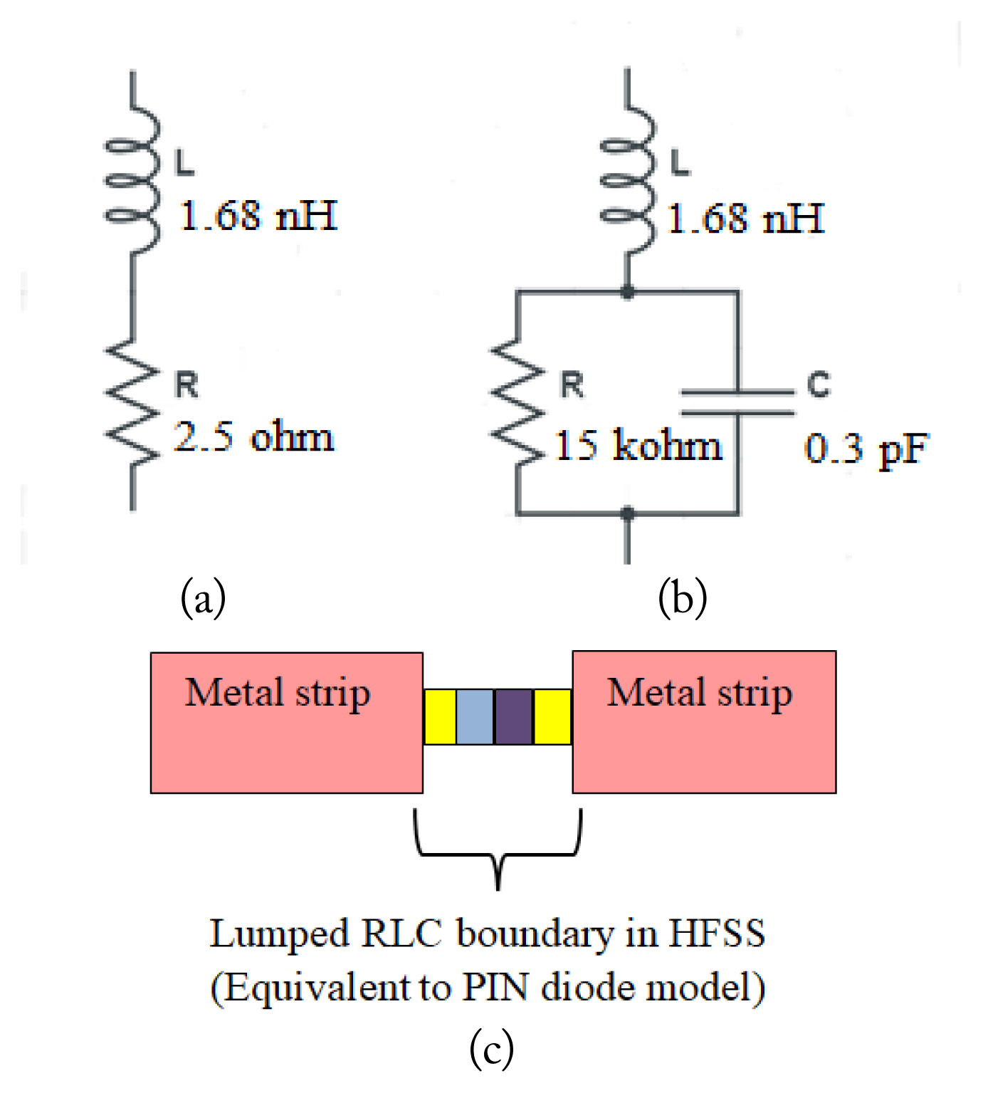
A PIN diode (NXP BAP64-03, 100 mA, 20 V) was employed for frequency reconfiguration in the proposed model. The equivalent circuits of the PIN diode in its ON and OFF states are shown in Fig. 2(a) and (b), respectively.
The three biasing states of a PIN diode are as follows: (i) zero DC, (ii) positive DC, and (iii) negative DC. In the simulation, the PIN diode was modelled as a lumped RLC equivalent. For zero DC bias, there was no connection between the two L-shaped rectangular patches (such that there was no electrical path between them). The lower L-shaped rectangular patch was the only active radiator. During positive DC bias, the diode represented a series combination of 2.5 ╬® resistance and 1.68 nH inductance (in the simulation). The lower value of R in the forward bias increased the current flow between the radiating strips. During reverse DC bias, the diode provided a parallel combination of 0.3 pF capacitance and 15 k╬® resistance in series with an inductance of 1.68 nH (in the simulation). The higher value of R during reverse bias restricted the current flow.
The inductor value was kept constant, as it did not have any significant effect on the current distribution. The values of R, L, and C were considered from the data sheet of the PIN diode model. These values were tuned in the given range, ensuring resonance was achieved in the desired frequency band. The assignment of a lumped RLC boundary in the simulation tool, Ansys HFSS, is shown in Fig 2(c). Bias voltages of 0, +3, and ŌłÆ3 V were applied to the circuit for the zero, forward, and reverse biases, respectively. Depending on the type of biasing, different resonant frequencies were obtained from the single antenna model, as indicated in Table 2.
4. Current Distribution
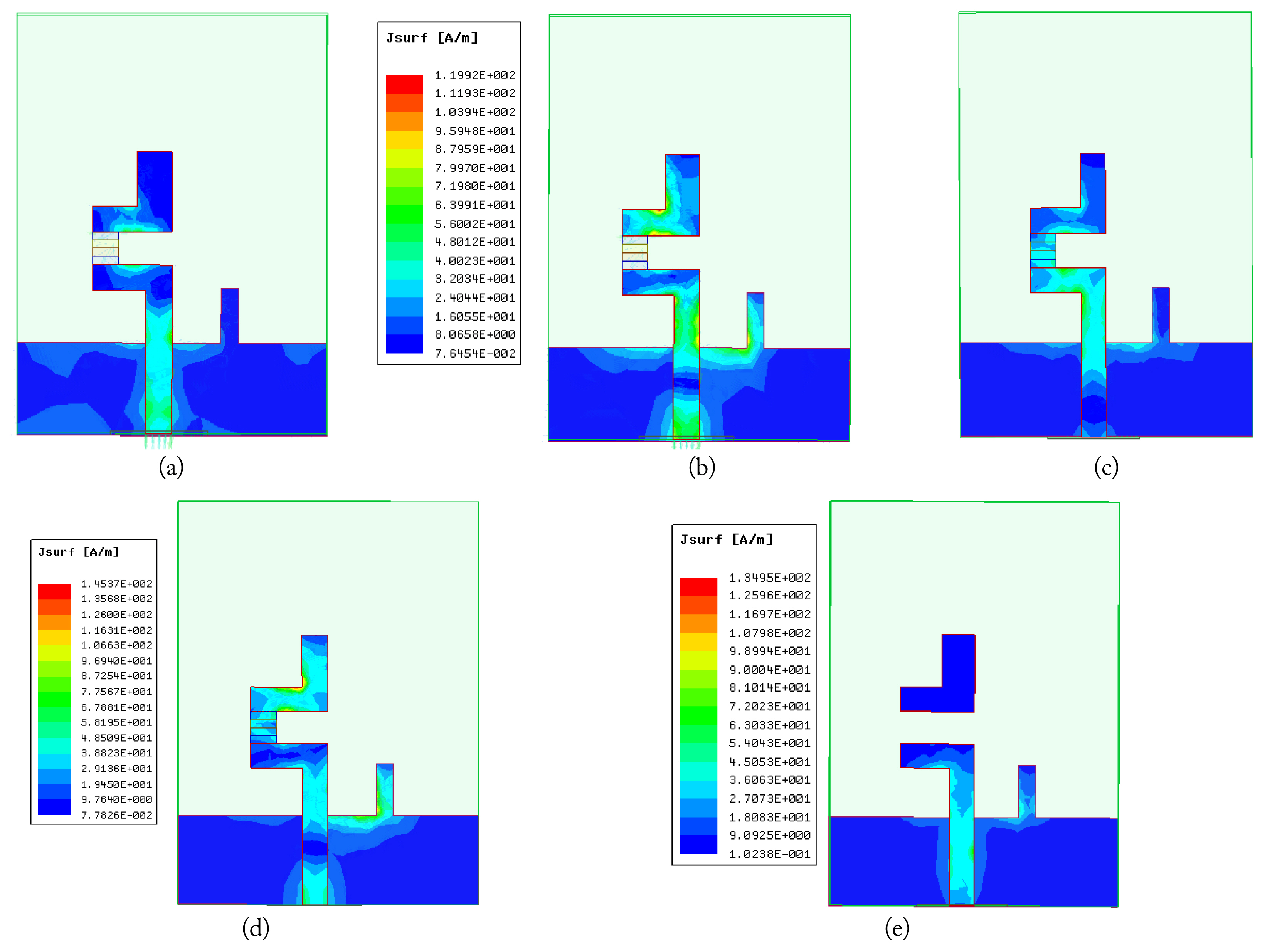
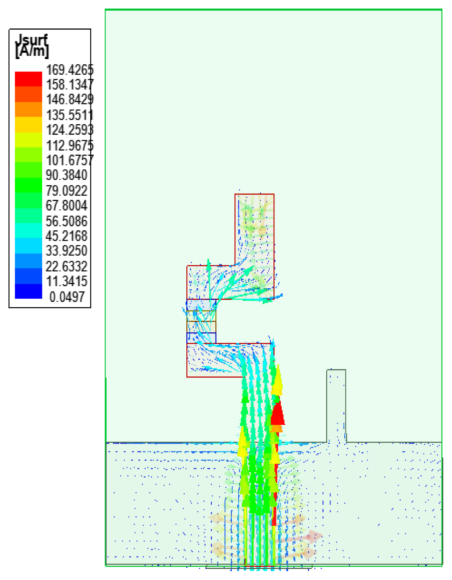
The proposed frequency reconfigurable antenna was simulated using Ansys HFSS. The far field radiation was mainly due to the current on the radiator. The simulated surface current densities at all five frequency bands are presented in Fig. 3. During forward bias, the antenna resonated at two frequencies. At the lower resonance, the surface current density was large on the lower L-shaped patch, as indicated in Fig. 3(a). The length of the lower L-shaped patch was 20 mm (i.e., c = 17 + e mm), in which most of the current was distributed in the lower part (i.e., c = 17 mm). The approximate length of the quarter wave at 2.4 GHz was calculated as 17 mm using the design Eqs. (1) and (2). This is illustrated using the vector surface current distribution at 2.4 GHz (phase 0┬░) in Fig. 4.
As indicated in Fig. 3(b), the surface current was distributed on the upper and lower L-shaped strips. It can also be observed that the surface current was distributed strongly around the stub. The length of the stub was slightly less than the quarter wavelength at 5.3 GHz. This rectangular stub on the ground plane played a vital role in achieving impedance matching at higher frequencies.
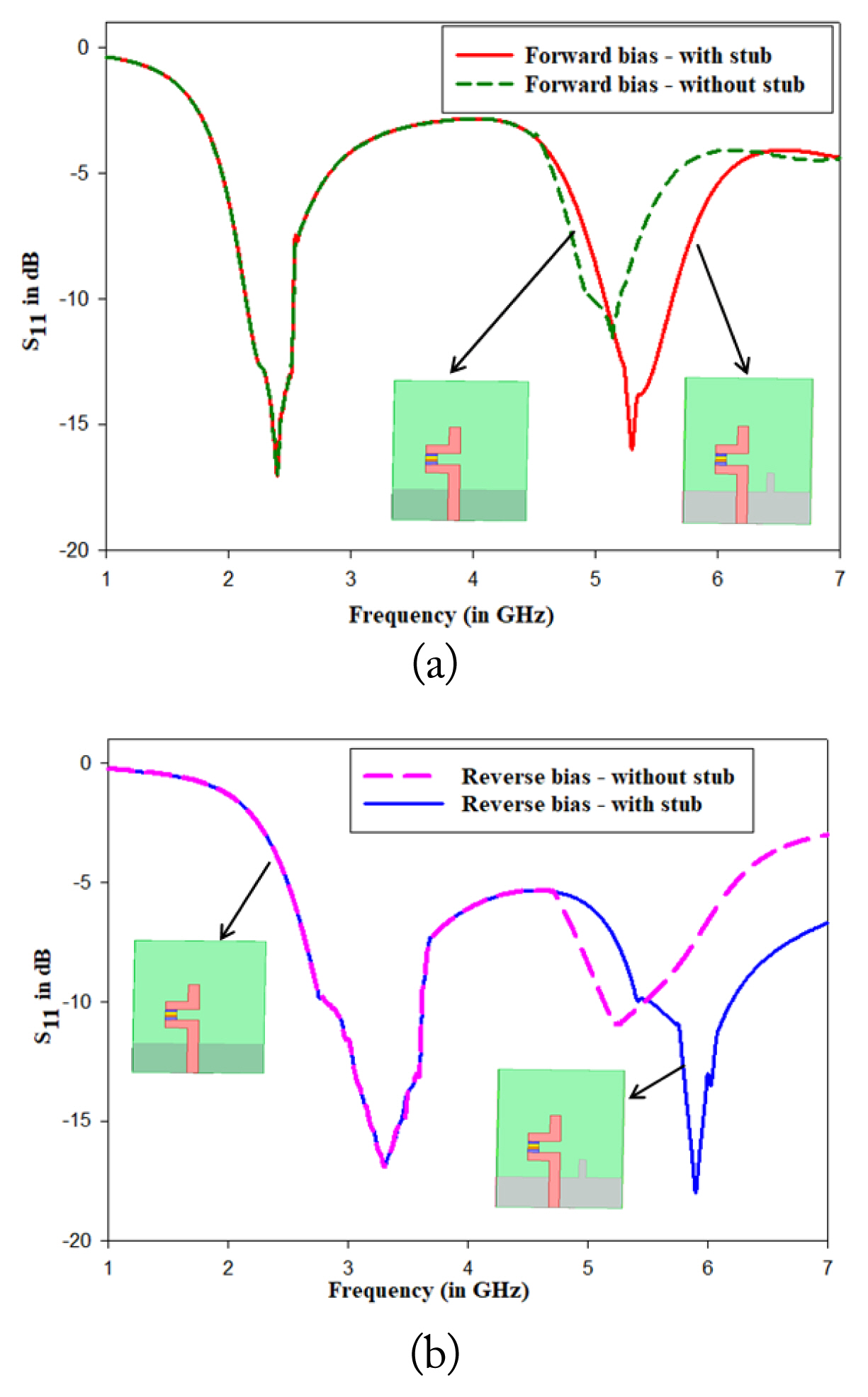
To illustrate the influence of the stub for impedance matching, the simulated reflection coefficient is plotted in Fig. 5.
With the rectangular stub, the antenna realized improved matching at the higher frequencies: 5.3 GHz in forward bias and 5.9 GHz in reverse bias.
III. Results and Discussion
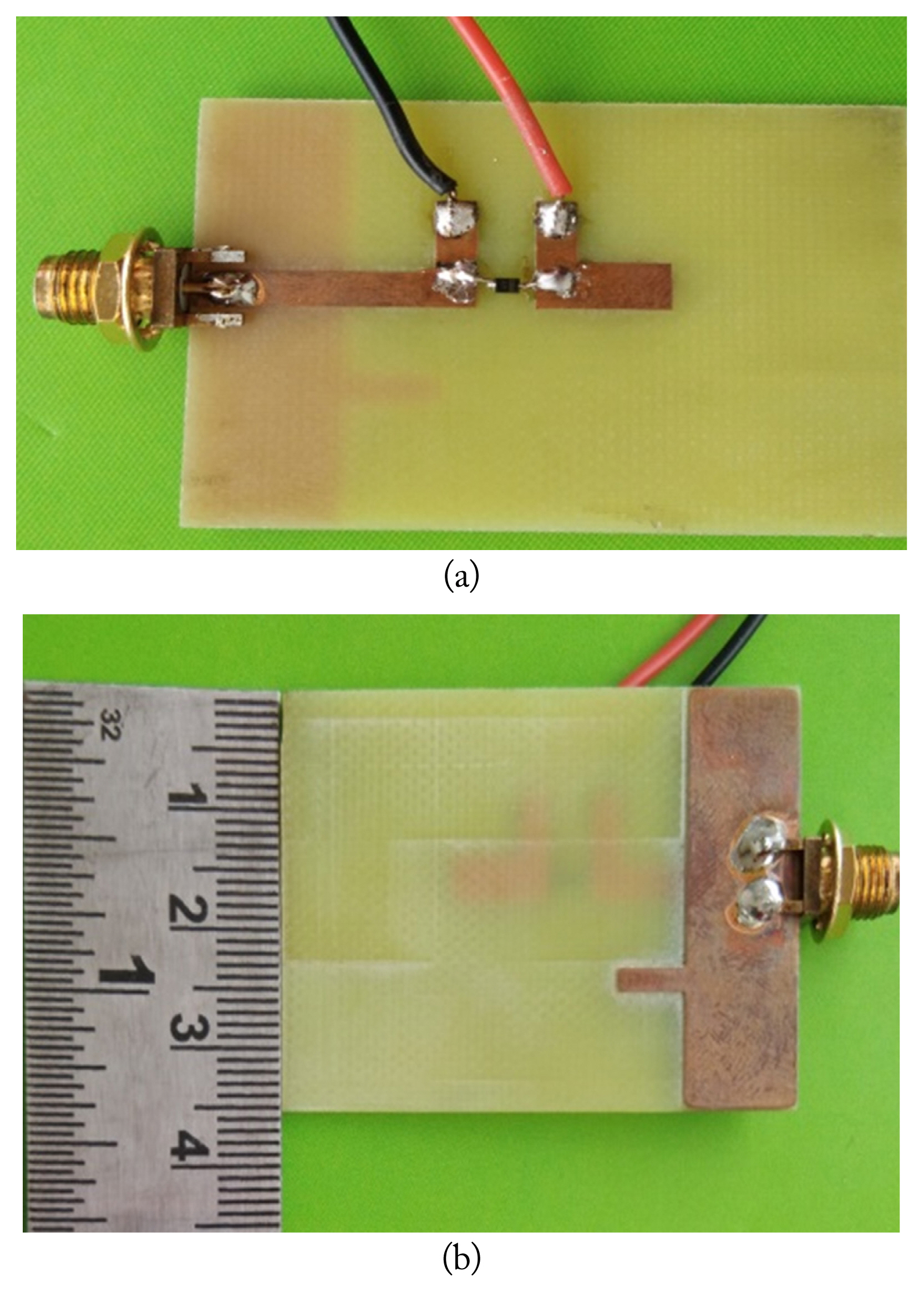
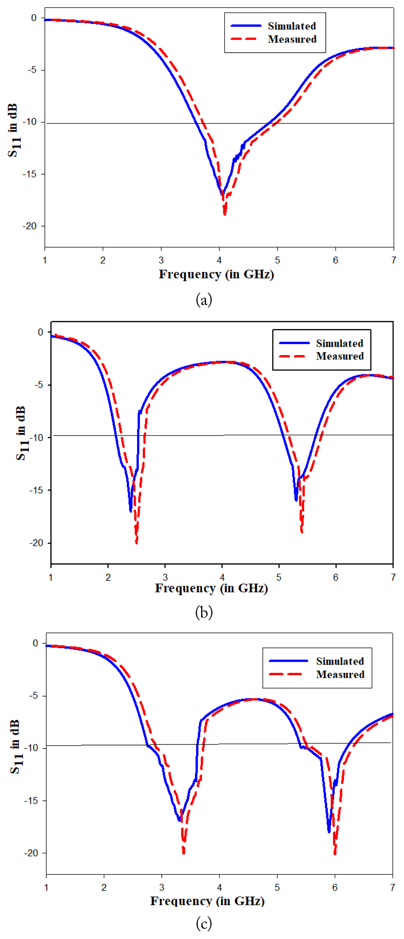
To validate the results, the model was fabricated and then measured using an Agilent vector network analyzer. A photograph of the fabricated antenna is presented in Fig. 6, while Fig. 7 displays a comparison between the simulated and measured return losses. The simulated antenna (at zero bias) achieved a ŌłÆ10 dB impedance bandwidth of 1.2 GHz (3.6ŌĆō4.8 GHz) with a center frequency at 4 GHz. During forward bias of the diode (+3 V), the antenna resonated at two frequencies: 2.4 GHz (2.1ŌĆō2.5 GHz) and 5.3 GHz (5ŌĆō5.6 GHz). During reverse bias of the diode (ŌłÆ3 V), the antenna resonated at 3.3 GHz (2.8ŌĆō3.6 GHz) and 5.9 GHz (5.5ŌĆō6.1 GHz).
The measured resonant frequency at zero bias was 4.1 GHz with a bandwidth of 3.7ŌĆō4.9 GHz. During forward bias, the antenna resonated at 2.47 GHz (2.2ŌĆō2.6 GHz) and 5.4 GHz (5.1ŌĆō5.7 GHz). During reverse bias, the antenna resonated at 3.38 GHz (2.8ŌĆō3.7 GHz) and 6 GHz (5.5ŌĆō6.3 GHz). The small deviation between the measured and simulated results could be due to minor fabrication errors and soldering losses in the SMA connector.
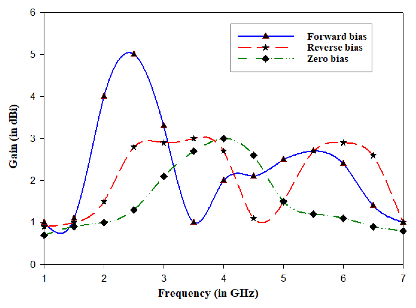
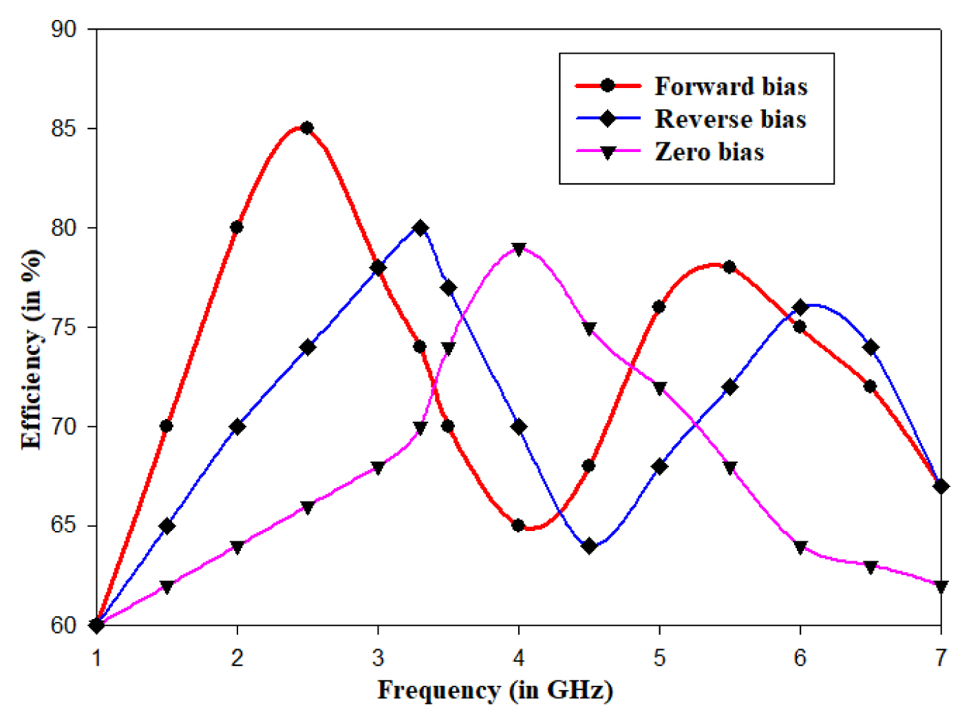
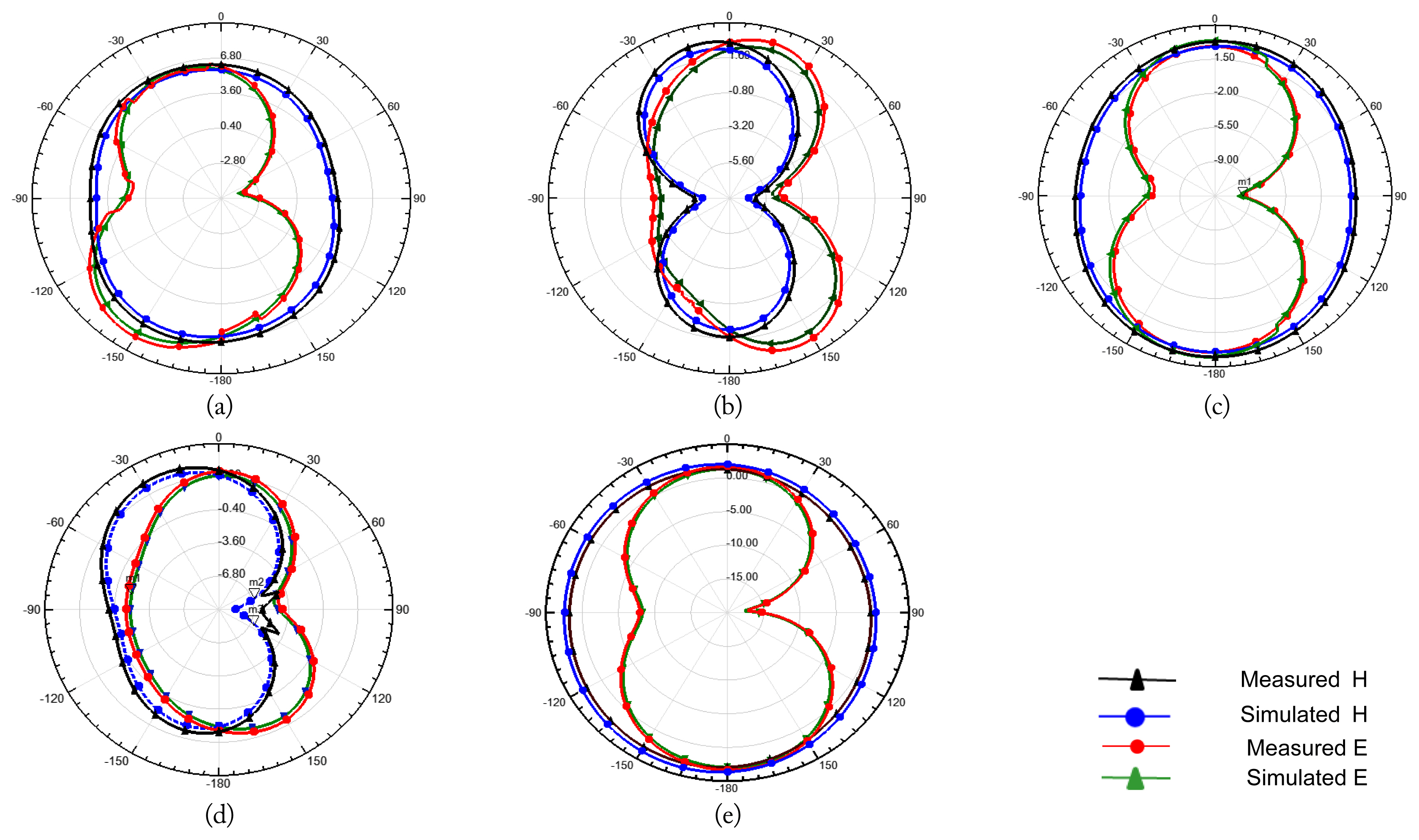
The measured gain at all resonant frequencies is displayed in Fig. 8. The gain varied between 2.6 and 5 dBi for the operating frequencies, which is acceptable for the previously mentioned applications. The efficiencies of the proposed antenna at all biasing conditions are displayed in Fig. 9. Further, the maximum and minimum radiation efficiencies were 85% and 76%, respectively. The simulated and measured E- and H-plane gain patterns at all five operating frequencies are presented in Fig. 10. It can be observed that the antenna radiated omni-directionally in the H-plane at 2.4, 6, and 4.1 GHz. All the E-plane patterns adopted a figure-of-8 shape, with a null lobe occurring at 90┬░. The simulated and measured patterns were in good agreement, with a minor difference of 0.5 dB.
IV. Conclusion
A simple and compact penta-band frequency-reconfigurable antenna is proposed in this paper. The presented patch antenna uses a single PIN diode connected between two rectangular strips. The various switching states of the PIN diode are responsible for achieving the desired operating frequency. It can operate at five frequency bands (2.4, 3.3, 5.3, 5.9, and 4 GHz), rendering it suitable for applications in WLAN and 5G. The antenna has acceptable ranges of gain from 2.6 to 5 dBi, and the maximum efficiency is 85%. This prototype was fabricated on easily available low-cost FR4 substrate, and the results were validated through measurements. The simulated results were in good agreement with the measured results.