J. Electromagn. Eng. Sci Search

CLOSE


J. Electromagn. Eng. Sci > Volume 20(4); 2020 > Article
Kim and Lee: Design of Wireless Power and Information Transfer Systems Considering Figure of Merit for Information

Abstract

Inductively coupled resonant wireless power transfer (WPT) systems can be used as a wireless power and information transfer (WPIT) system by properly adding the function of varying Rx loads. A new metric for the figure of merit for information transfer from Rx to Tx is proposed as the ratio of Tx input impedances for the Rx shorted and optimum loads to systematically assess the information transfer. While most of WPT and near-field communication (NFC) devices have been adopted for very short distances between Tx and Rx, this work shows that the WPIT systems using inductively coupled resonant structures with high Q-factor coils enable much longer working distances with the best power transfer efficiency and information transfer capability. Several design examples show that the newly proposed figure of merit for information transfer is an essential metric in the understanding and design of WPIT systems. The theory is validated with circuit and electromagnetic simulations for various system configurations.

I. Introduction

Wireless power transfer (WPT) based on inductively coupled resonance was first introduced in [1], where an efficiency of about 40% was achieved with a separation of approximately 2 m between Tx and Rx of spiral shapes. Since then, the inductively coupled resonant WPT technology has been developed in theory and also applied to many applications including WPTs to multiple receivers, electric mobile phones, home appliances, motor vehicles, biomedical devices, and so on [26]. In most practical WPT devices, the information of power-receiving units needs to be transferred to power-transmitting units. There may be a variety of information but the identification numbers, stored power levels, etc., are essentially required in the basic operation of WPT devices. To cope with this necessity, the simultaneous wireless and information power transfer (SWIPT) has been studied in various forms of geometry and for the possible merging of information and power in the near future [710]. However, most of the research papers in this area focus on the numerous architectures in the high level of the hierarchy. However, some papers focusing on actual structures enabling information transfer in the current WPT frame are at times available, under the name of wireless power and information transfer (WPIT).
In [11], theory of high-order modulation for near-field RF identification (RFID) and WPT was presented. A system that transmits power using a triangular current waveform and transmits information to its third-order harmonic was reported in [12]. In [13], a WPIT technology based on binary frequency shift keying modulation using the dual bands of a series-parallel combined resonant circuit was proposed. Its experimental prototype exhibited a communication rate up to 20 kbps, while maintaining a power transfer efficiency greater than 85% at a distance of 50 mm. However, these systems are complex in configuration. In [14], a frequency-agile load modulation scheme was proposed for a reliable near-field magnetic resonance WPT system. A wireless power and bidirectional data transmission scheme through mutual coupling between two isolated LC resonators was proposed in [15]. The near-field communication (NFC) [16] used for RFID technology may also be promising for delivery of this information by means of load modulation techniques. The existing NFC and other WPIT demonstrations are practically limited within a distance of several centimeters.
In this paper, we use simple mathematical expressions to analyze a WPIT system in terms of power and information transfer capabilities. Then, we provide design equations for a specifically required efficiency and transfer capability of Rx status information. Especially, to assess the information (including Rx status) transfer capability from Rx to Tx in a systematic manner, we propose a new metric using the input impedances at the Tx terminal depending on Rx loads. Its effectiveness and usefulness is validated by several design examples.
In Section II, the WPT performance of a single-input multiple-output (SIMO) system in terms of input impedances, efficiencies, and optimum loads for maximum efficiency are briefly discussed. Then, we newly define the figure of merit for information delivery using Tx input impedance variations depending on Rx load variations and demonstrate its usefulness. In Section III, we present some practical examples to validate the proposed WPIT methodology with electromagnetic (EM)-simulated results. The conclusions and closing comments are in Section IV.

II. Design Theory

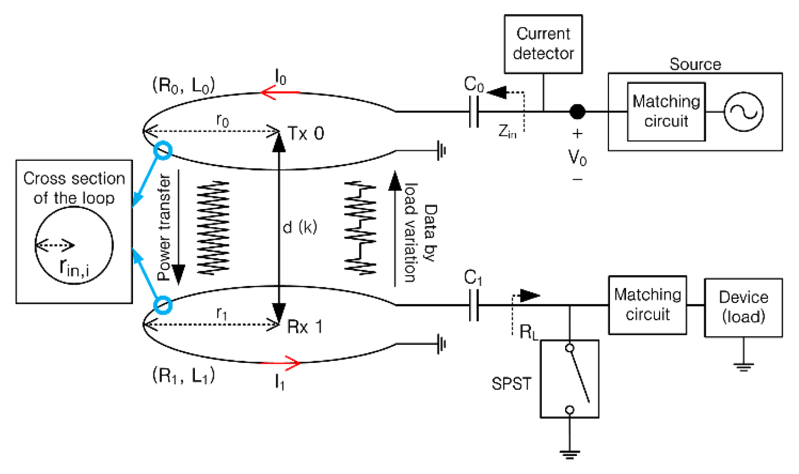
Fig. 1 shows the equivalent circuit of a WPIT system. The system is composed of Tx0 (or Tx) and Rx1 (or Rx) coils (or loops), which may be a single turn loop or a multi-turn loop or a spiral coil, separated by a certain distance d. The loops, having inductances, are loaded with capacitors for LC resonance. The power is transferred from Tx to Rx via magnetically coupled resonant loops. Ri and Li are the resistance and inductance of the Tx (i = 0) and Rx (i = 1) loops, respectively. Ci is the capacitance of the lumped capacitor for Tx (i = 0) and Rx (i = 1), respectively. ri is the radius of the ith loop and rin,i is the inner radius of the ith loop wire. V0 is the voltage at the input. The single-pole single-through (SPST) switch is operated between off (for an optimum load) and on (for a shorted load). The usual function of the Rx matching circuit is to transform the usually small Rx optimum load to the large device load (say, 50 Ω). Conventional WPT has been made with the switch off to achieve maximum efficiency. The Rx status information (such as a device identity, energy charged levels, etc.) can be transferred from Rx to Tx by switching between the on and off states of the SPST. Based on this equivalent circuit, the system is usually formulated by a Z-matrix given by
(1)
[V00]=[Z00Z01Z10Z11][I0I1]=[R0+jωL0+1jωC0-jωkL0L1-jωkL0L1R1+RL+jωL1+1jωC1][I0I1]
where k is the coupling coefficient between Tx and Rx loops [17]. It is well known that k approaches 1 as the distance between Tx and Rx becomes 0 and it approaches 0 as the distance between Tx and Rx becomes very large. V0 is the source voltage, RL is the Rx load resistance, and ω is the angular frequency. I0 and I1 are the currents on loop 1 and 2, respectively. The ratio of currents on Tx and Rx loops is given by [18]:
(2)
I1I0=jωkL0L1R1+RL+jωL1+1jωC1.
It is observed that as RL increases, (2) becomes small and approaches 0 as RL goes to infinity (open). The phase of the current flowing on Rx (I1) is 90° ahead of that flowing on Tx (I0) following Faraday’s law. The input impedance is defined as the ratio of V0 and I0 on a Tx terminal and expressed as
(3)
Zin(ω,RL)=V0I0=Z00+Z01I1I0=R0+jωL0+1jωC0+(ωk)2L0L1R1+RL+jωL1+1jωC1.
At the resonant frequency, the input impedance (3) reduces to
(4)
Zin(ω0,RL)=R0+(ω0k)2L0L1R1(1+RL/R1).
If we define the figure of merit for the power transfer (F) as
(5)
F=kQ0Q1=kQ(Q0=ω0L0R0,Q1=ω0L1R0),
the input impedance (4) at the resonant frequency depending on the Rx load RL can be re-written as
(6)
Zin=R0(1+F21+RL/R1),
which is a purely real number. At this point, the essential part of power transfer efficiency for a resonant WPT system needs to be summarized [17]. The efficiency can be stated in a simple manner by
(7)
η(F,b)=F2(1+b1+F2)(1+1b1+F2),
where b is the deviation factor against the Rx optimum load RL,opt defined by
(8)
b=RLRL,opt=RLR11+F2.
A short observation of (7) tells that it is a function of the figure of merit for power transfer (F) and b, and a large F is merely a necessary condition for a high efficiency. The maximum efficiency is guaranteed with the additional condition of b=1(RL=RL,opt=R11+F2).
Now, we examine the ways of transferring Rx status information (or others) to Tx. Monitoring (6) at the Tx terminal depending on RL is just like monitoring the current on Tx (I0) depending on RL since I0 = V0/Zin. When RL = 0 (short), the system is at the over-coupled limit, no power is transferred to Rx, and the efficiency (7) is 0. However, the largest current is induced on Rx and the magnetic flux back to Tx affects the Tx input impedance most significantly, and the input impedance becomes the largest: R0(1 + F2). With this, the Tx current I0 becomes the smallest. When RL = ∞ (open), no current is induced on the Rx loop, the system is at the under-coupled limit, no power is transferred to Rx, the efficiency (7) is also 0, the Tx is as if being isolated from Rx, and the Tx input impedance becomes that of its own: R0. When RL=RL,opt=R11+F2(b=1) (optimum for maximum efficiency), (6) becomes
(9)
Zin=R0(1+F21+1+F2)=R01+F2.
The current variations on Tx (or the input impedance variations) depending on RL (open, short, optimum) can be used for the information transfer from Rx to Tx. These input impedances (6) and the power transfer efficiencies (7) are summarized in Table 1.
NFC [16] more or less utilizes these variations of Zin at the Tx terminal occurring between the two load states of Rx, but mostly at a close proximity of Tx to Rx. Using the results in Table 1, we can assess the transfer capability of Rx information for the usual resonant WPT systems.
The best choice of the Rx load set for information transfer from Rx to Tx may be the short (over-coupled limit) and open (under-coupled limit) states, since this results in the largest current variation at the Tx with the effect of a lowest bit error rate. However, it is noted that with this choice, power is not transferred to Rx. The best Rx load choice for WPIT may be the short (for the greatest magnetic flux effect to Tx) and optimum (for the highest power transfer efficiency) loads. The real resistance of the SPST switch (Fig. 1) for the short state is not exactly 0. The practical resistance is about 10 mΩ but does not much affect the results in Table 1.
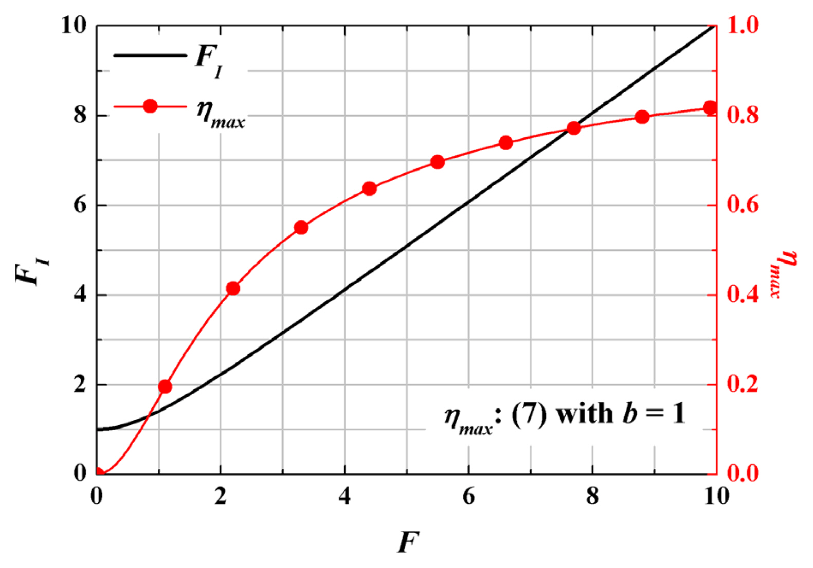
For the purpose of quantitative assessment by a new metric, we define the figure of merit for Rx information transfer to Tx (FI) as a ratio of the Tx Zin when RL = 0 and the same when RL = RL,opt in Table 1, given by
(10)
FI=Zin(RL=0)Zin(RL=RL,opt)=1+F2.
The figure of merit for Rx information transfer to Tx (FI) as defined in (10) also corresponds to the current (I0) variation at the Tx terminal depending on Rx loads of “short” and “optimum” RL since I0 = V0/Zin. The metric (10) is plotted in Fig. 2 together with the maximum efficiencies as a function of the figure of merit for power transfer (F). We can see that as the figure of merit for power (F) increases, the figure of merit for information transfer (FI) also increases and the power transfer efficiency also increases. Notice that when F is roughly larger than 3, the efficiency is greater than 50% and FI almost ap proaches F. Taking an example, the transfer efficiency of about 80% is achieved with F = 9, where FI is also about 9.

III. Design Examples Validated with Electromagnetic Simulations

The real resonant WPT systems realized for an F given by (5) are numerous. Several realizations for a system consisting of a Tx loop with r0 = 10 cm and a Rx loop with r0 = 5 cm are shown in Table 2, where the quality factor Q is the geometrical mean of Q0 and Q1 (5). The coupling coefficients k were obtained using [16].
In Table 3, we summarize the same as in Table 2 but for a different system with larger Tx and Rx loops with r0 = r1 = 20 cm, enabling power and information transfer in longer ranges. It is seen in Table 3 that an efficiency of 56% is achieved for the case of d = 80 cm with FIF = 7.3. The figure of merit for power (F), one important parameter in the resonant WPT efficiency, can now be understood as the Tx current variations used for Rx information transfer.
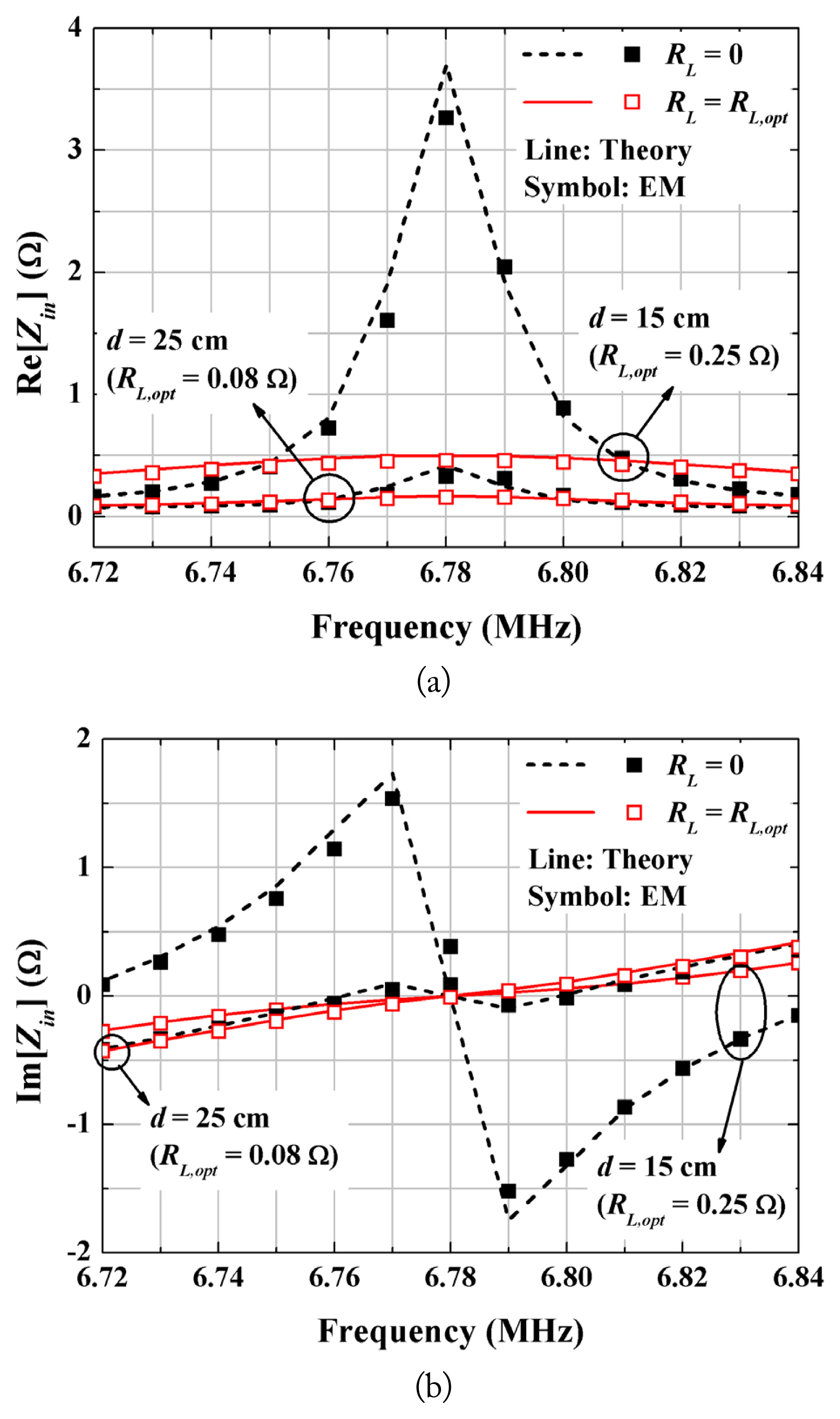
We take the two system configurations with d = 15 cm and 25 cm in Table 2 and plot the real part (a) and imaginary part (b) of the input impedance (3) for different loads of RL = 0 and RL=RL,opt=R11+F2 as a function of frequency in Fig. 3. The radii of Tx and Rx loops are 10 cm (Q0 = 388.8) and 5 cm (Q1 = 334.2), respectively. The Tx and Rx loop wire radii are 0.1 cm. The imaginary parts (b) of the input impedances for both cases of d = 15 cm and d = 25 cm are observed to be zero at the resonant frequency since the system is at resonance. The real parts (a) of the input impedances at the resonant frequency, given by (6) and in Table 1, have the maximums when RL = 0. The circuit-simulated figures of merit for information transfer (FI) are 3.7/0.5 (= 7.38) for the case of d = 15 cm and 0.42/0.17 (= 2.48) for the case of d = 25 cm. The EM-simulated figures of merit for information transfer (FI) are 3.26/0.45 (= 7.2) for the case of d = 15 cm and 0.33/0.16 (= 2.1) for the case of d = 25 cm. The results are in agreement with the theoretical ones of 7.4 and 2.5 in Table 2. These FIs should be understood as the Tx current variations due to the Rx load changes. The overall EM-simulated input impedances are shown to be in good agreement with the theoretical ones.
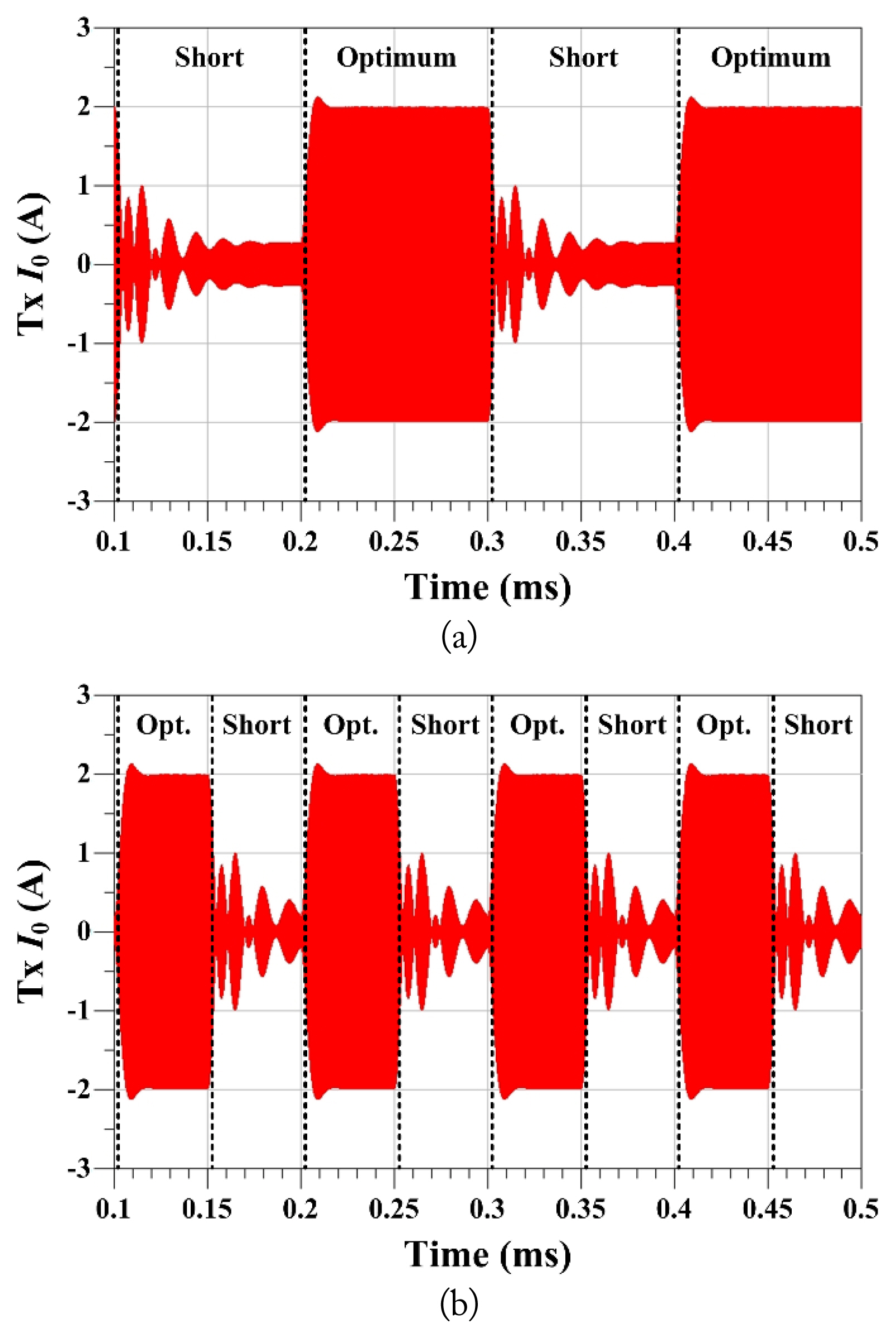
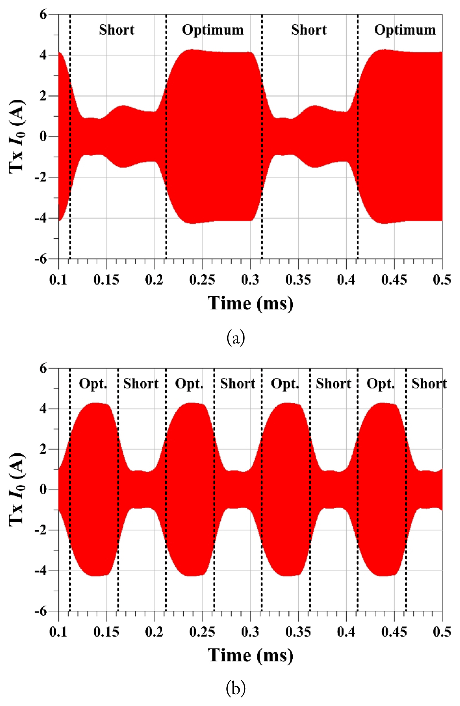
Fig. 4 shows the transient responses of the Tx currents when the Rx load switches between with RL = 0 and RL=RL,opt=R11+F2 with 10 kbps (a) and 20 kbps (b) for the case of d = 15 cm and Q=Q0Q1=360.5 in Table 2. Based on the AC steady state analysis, the Tx current variation (characterized by FI) with each Rx load has been found to be almost identical to the theoretical value of 7.4. Based on the transient analysis with increasing switching rates, Fig. 4(a) and 4(b) show that it takes about 0.5 ms for the Tx current to reach a steady state. The source voltage V0 in Fig. 1 is assumed to be 1 V. For the shorted Rx load with RL = 0 Ω and optimum load with RL = 0.25 Ω, the average Tx current envelopes are 0.33 A and 1.97 A, respectively, for the case of the 10 kbps switching rate (Fig. 4(a)). Thus, the ratio of the Tx currents is 6.0 (= 1.97/0.33). For the case of 20 kbps (Fig. 4(b)), the ratio of the Tx current envelopes is 5.0 (= 1.96/0.39). Even though the ratio of Tx currents somewhat deviates from the expected FI due to the effects of the transients from switching operations.
Fig. 5 shows the same as plotted in Fig. 4 for the different configuration of d = 80 cm and Q=Q0Q1=776.2(F=3.4,FI=3.6) in Table 3. The Tx current variation with the mentioned two Rx loads when reached in steady state is about 3.5 (close to the theoretical FI of 3.6). The source voltage V0 in Fig. 1 is assumed to be 1 V. The short and optimum loads (RLs) are 0 Ω and 0.24 Ω. The ratio of Tx current envelopes is 3.3 for the case of 10 kbps and 3.1 for the case of 20 kbps, again close to the theoretical value (FI) of 3.6.
The figure of merit for information transfer (FI) as defined in (10), expressed as a function of the figure of merit for power transfer (F), has been shown to be very useful in characterizing and estimating the resonant WPIT systems, especially in their capability of transferring Rx information to Tx.

IV. Conclusion

A new metric named “a figure of merit for information transfer” has been defined to assess WPIT systems in their capability to transfer information from Rx to Tx. Its usefulness has been verified for several WPIT system configurations with wide ranges of Tx to Rx distances. It has been found to be close to the figure of merit for power and shown to be the ratio of the Tx currents when the Rx load is shorted and optimum. Introduction of the new metric is expected to put a basic foundation in the evaluation of WPIT systems which started being developed recently.

Acknowledgments

This research was supported by the Ministry of Science, ICT and Future Planning, Korea, under the Information Technology Research Center support program (No. IITP-2020-2016-0-00291) supervised by the IITP (National IT Industry Promotion Agency).

Fig. 1
Configuration of a magnetically coupled wireless power and information transfer (WPIT) system.
jees-2020-20-4-241f1.jpg
Fig. 2
Figure of merit for Rx information transfer to Tx (FI) and maximum efficiency (ηmax) at the resonant frequency as a function of figure of merit for power (F) for a WPIT system.
jees-2020-20-4-241f2.jpg
Fig. 3
Input impedances of SISO system for different loads (r0 = 10 cm, r1 = 5 cm, rin0 = rin1 = 0.1 cm, Q1 = 388.81, and Q2 = 334.23): (a) real parts and (b) imaginary parts.
jees-2020-20-4-241f3.jpg
Fig. 4
Circuit-simulated transient Tx current (I0) for different Rx loads with 0 (short) and 0.25 Ω (optimum) (V0 = 1 V, frequency = 6.78 MHz, r0 = 10 cm, r1 = 5 cm, rin0 = rin1 = 0.1 cm, Q1 = 388.8, Q2 = 334.2, d = 15 cm, k = 0.0203, and F = 7.3): (a) data rate = 10 kbps and (b) data rate = 20 kbps.
jees-2020-20-4-241f4.jpg
Fig. 5
Circuit-simulated transient Tx current (I0) for different Rx loads with 0 (short) and 0.24 Ω (optimum) (V0 = 1 V, frequency = 6.78 MHz, r0 = r1 = 20 cm, rin0 = rin1 = 0.2 cm, Q1 = Q2 = 776.2, d = 80 cm, k = 0.0044, and F = 3.4): (a) data rate = 10 kbps and (b) data rate = 20 kbps.
jees-2020-20-4-241f5.jpg
Table 1
Input impedances and transfer efficiencies depending on Rx loads at resonant frequency
Load status RL (Ω) b Zin(ω0) (Ω) η(ω0)
Short (over-coupled limit) 0 0 R0(1 + F2) 0
Optimum (critically-coupled) R11+F2 1 R01+F2 F2(1+1+F2)2
Open (under-coupled limit) R0 0
Table 2
Examples of design system configurations (r0 = 10 cm, r1 = 5 cm, rin0 = rin1 = 0.1 cm, Q1 = 388.81, and Q2 = 334.23)
d (cm) k Q F FI ηmax (%)
5 0.0904 360.5 32.6 32.6 94.0
10 0.0419 360.5 15.1 15.1 87.6
15 0.0203 360.5 7.3 7.4 76.1
20 0.0108 360.5 3.9 4.0 60.2
25 0.0063 360.5 2.3 2.5 42.4
30 0.0039 360.5 1.4 1.7 26.7
Table 3
Examples of design system configurations (r0 = r1 = 20 cm, rin0 = rin1 = 0.2 cm, Q0 = Q1 = 776.2)
d (cm) k Q F FI ηmax (%)
10 0.1882 776.2 146.1 146.1 98.6
20 0.0836 64.9 64.9 97.0
40 0.0240 18.6 18.7 89.8
60 0.0093 7.2 7.3 75.9
80 0.0044 3.4 3.6 56.1
100 0.0024 1.9 2.1 35.6

References

1. R Moffatt Kurs and M Soljacic, "Simultaneous mid-range power transfer to multiple devices," Applied Physics Letters, vol. 96, no. 4, article 044102, 2010.
crossref
2. S Kim, S Hwang, S Kim, and B Lee, "Investigation of single-input multiple-output wireless power transfer systems based on optimization of receiver loads for maximum efficiencies," Journal of Electromagnetic Engineering and Science, vol. 18, no. 3, pp. 145–153, 2018.
crossref pdf
3. S Cheon, YH Kim, SY Kang, ML Lee, JM Lee, and T Zyung, "Circuit-model-based analysis of a wireless energy-transfer system via coupled magnetic resonances," IEEE Transactions on Industrial Electronics, vol. 58, no. 7, pp. 2906–2914, 2011.
crossref
4. AK RamRakhyani, S Mirabbasi, and M Chiao, "Design and optimization of resonance-based efficient wireless power delivery systems for biomedical implants," IEEE Transactions on Biomedical Circuits and Systems, vol. 5, no. 1, pp. 48–63, 2011.
crossref pmid
5. JH Choi, SK Yeo, S Park, JS Lee, and GH Cho, "Resonant regulating rectifiers (3R) operating for 6.78 MHz resonant wireless power transfer (RWPT)," IEEE Journal of Solid-State Circuits, vol. 48, no. 12, pp. 2989–3001, 2013.
crossref
6. Y Zhang, T Lu, Z Zhao, F He, K Chen, and L Yuan, "Selective wireless power transfer to multiple loads using receivers of different resonant frequencies," IEEE Transactions on Power Electronics, vol. 30, no. 11, pp. 6001–6005, 2015.
crossref
7. I Krikidis, S Timotheou, S Nikolaou, G Zheng, DWK Ng, and R Schober, "Simultaneous wireless information and power transfer in modern communication systems," IEEE Communications Magazine, vol. 52, no. 11, pp. 104–110, 2014.
crossref
8. CF Liu, M Maso, S Lakshminarayana, CH Lee, and TQ Quek, "Simultaneous wireless information and power transfer under different CSI acquisition schemes," IEEE Transactions on Wireless Communications, vol. 14, no. 4, pp. 1911–1926, 2015.
crossref
9. TDP Perera, DNK Jayakody, SK Sharma, S Chatzinotas, and J Li, "Simultaneous wireless information and power transfer (SWIPT): recent advances and future challenges," IEEE Communications Surveys & Tutorials, vol. 20, no. 1, pp. 264–302, 2018.
crossref
10. DKP Asiedu, S Mahama, SW Jeon, and KJ Lee, "Optimal power splitting for simultaneous wireless information and power transfer in amplify-and-forward multiple-relay Systems," IEEE Access, vol. 6, pp. 3459–2468, 2018.
crossref
11. J Besnoff, M Abbasi, and DS Ricketts, "High data-rate communication in near-field RFID and wireless power using higher order modulation," IEEE Transactions on Microwave Theory and Techniques, vol. 64, no. 2, pp. 401–413, 2016.
crossref
12. Z Yan, Z Xiang, L Wu, and B Wang, "Study of wireless power and information transmission technology based on the triangular current waveform," IEEE Transactions on Power Electronics, vol. 33, no. 2, pp. 1368–1377, 2018.
crossref
13. JG Kim, G Wei, MH Kim, HS Ryo, and C Zhu, "A wireless power and information simultaneous transfer technology based on 2FSK modulation using the dual bands of series-parallel combined resonant circuit," IEEE Transactions on Power Electronics, vol. 34, no. 3, pp. 2956–2965, 2018.
crossref
14. NY Kim, SW Yoon, and CW Kim, "Frequency-agile load-modulated magnetic resonance wireless power transfer system for reliable near-field in-band signalling," Electronics Letters, vol. 49, no. 24, pp. 1558–1559, 2013.
crossref
15. CC Huang and CL Lin, "Wireless power and bidirectional data transfer scheme for battery charger," IEEE Transactions on Power Electronics, vol. 33, no. 6, pp. 4679–4689, 2018.
crossref
16. JI Cairo, J Bonache, F Paredes, and F Martin, "Reconfigurable system for wireless power transfer (WPT) and near field communications (NFC)," IEEE Journal of Radio Frequency Identification, vol. 1, no. 4, pp. 253–259, 2017.
crossref
17. G Kim and B Lee, "Alternative expressions for mutual inductance and coupling coefficient applied in wireless power transfer," Journal of Electromagnetic Engineering and Science, vol. 16, no. 2, pp. 112–118, 2016.
crossref pdf
18. G Kim, S Boo, S Kim, and B Lee, "Control of power distribution for multiple receivers in SIMO wireless power transfer system," Journal of Electromagnetic Engineering and Science, vol. 18, no. 4, pp. 221–230, 2018.
crossref pdf

Biography

jees-2020-20-4-241f6.jpg
Gunyoung Kim received a B.S. in Radio Communication Engineering from Kyung Hee University, Yongin, Korea in 2010, an M.S. in Electronics and Radio Engineering from Kyung Hee University in 2012, and a Ph.D. in Electronic Engineering from Kyung Hee University in 2018. He is currently working at Hanwha Systems. His fields of research include microwave antennas, phased array antenna, and radar systems.

Biography

jees-2020-20-4-241f7.jpg
Bomson Lee received the B.S. degree in Electrical Engineering from Seoul National University, Seoul, Korea, in 1982. From 1982 to 1988, he was with the Hyundai Engineering Company Ltd., Seoul, Korea. He received the M.S. and Ph.D. degrees in Electrical Engineering from the University of Nebraska, Lincoln, NE, USA, in 1991 and 1995, respectively. In 1995, he joined the faculty at Kyung Hee University, where he is currently a professor in the Department of Electronic Engineering. From 2007 to 2008, he was the chair of the technical group for microwave and radio wave propagation in the Korea Institute of Electromagnetic Engineering & Science (KIEES). In 2010, he was an editor-inchief of the Journal of the Korean Institute of Electromagnetic Engineering and Science. In 2018, he served as the president of KIEES. His research activities include microwave antennas, RF identification (RFID) tags, microwave passive devices, wireless power transfer, and metamaterials.

ABOUT
ARTICLE CATEGORY

Browse all articles >

BROWSE ARTICLES
AUTHOR INFORMATION
Editorial Office
#706 Totoo Valley, 217 Saechang-ro, Yongsan-gu, Seoul 04376, Korea
Tel: +82-2-337-9666    Fax: +82-2-6390-7550    E-mail: admin-jees@kiees.or.kr                

Copyright © 2024 by The Korean Institute of Electromagnetic Engineering and Science.

Developed in M2PI

Close layer
prev next