


I. Introduction
Recent developments in mobile communication technology gave rise to a bandwidth requirement of 300 MHz (11.7%) for the 3.5 GHz frequency band used for 5G technology. To meet this requirement, developers created many multiple-input, multiple-output antennas, which are mainly used in mobile communication [1, 2]. These antennas, however, need additional space for multiple ports, making it difficult to satisfy the required bandwidth with a single antenna port in a given space. This problem was overcome through the development of frequency-tunable antennas. A variant of these innovations is the two-dimensional printed inverted-F antenna (PIFA), which is widely used in electronic devices as a communication antenna [3]. It can be easily fabricated through modern printing technology and fitted into a limited space because of its low-profile structure. Another example is the frequency-tunable planar inverted-F antenna equipped with a capacitor [4ŌĆō7] (see also [8]). The capacitor is located between the main radiator and a parasitic element to vary resonant frequencies, after which capacitance is modified. This design means that the space occupied by a complex feeding structure expands because the antenna is directly connected to the radiator and parasitic element. An important consideration, however, is that using different capacitance values can contribute to antenna losses.
Previously developed frequency-reconfigurable antennas are equipped with yttrium-iron-garnet elements, and their resonant frequencies are tuned by changing the magnetic field, which is controlled by a DC bias [9]. The drawback to this design is that it reduces an antennaŌĆÖs radiation efficiency and increases fabrication costs.
In the present study, a frequency-tunable PIFA (FTPIFA) comprising a perturbed parasitic element was designed, with mobile devices as reference. The size of the antenna was reduced on the basis of perturbation theory [10ŌĆō12] to the radiation element. The resonant frequency of the PIFA can be tuned by changing the volume of the electric and magnetic fields.
II. Antenna Design
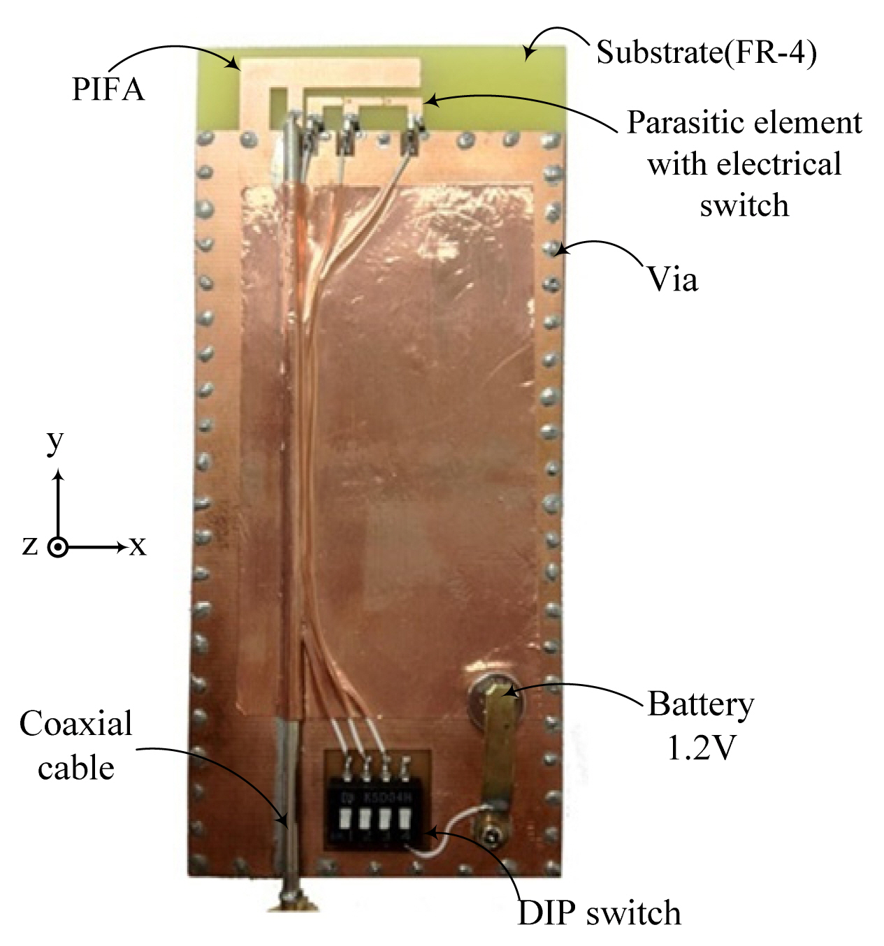
Fig. 1(a) and (b) show the designed PIFA with a parasitic element between the radiator and the ground plane. It was printed on a 0.8-mm thick, 50 ├Ś 100 mm2 FR-4 (╔ør = 4.3, tan╬┤ = 0.025) substrate. The size of the antennaŌĆÖs radiator is 24.8 ├Ś 10 mm2. Because the position where a short circuit occurs (ŌĆ£short positionŌĆØ hereafter) can be tuned from switches #1 to #5 by using a copper strip, the central frequency (2,045 MHz) is based on the shorted state of switch #3.
Fig. 1(c) illustrates the new antenna structure used to change the short-circuit structure of the copper strip (Fig. 1(b)). A PIN diode (SMP1345-079LF) located between the parasitic element and the ground plane functions as a switch. It was redesigned by adding meandered gaps to the parasitic element for DC blocking and the independent operation of each switch.
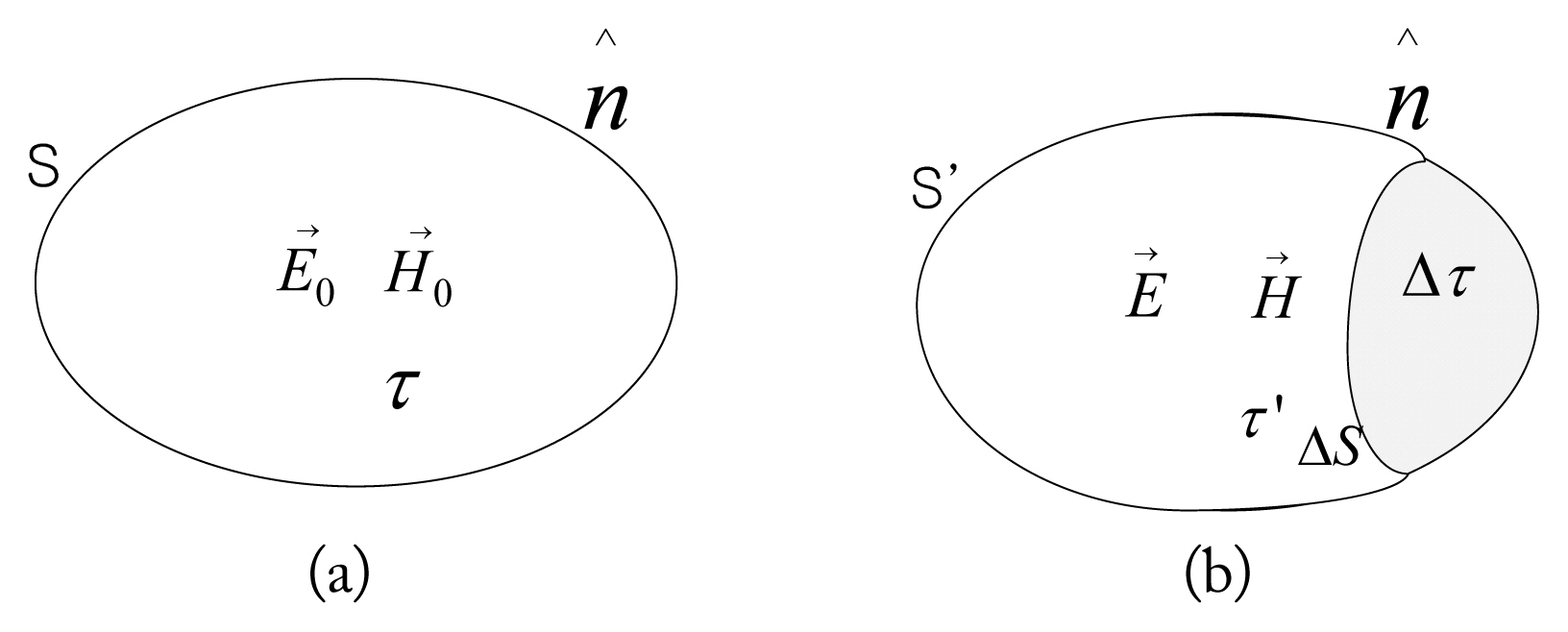
The principles used to design the antenna are those underlying the perturbation method [11], through which resonant frequency can be controlled by changing the volume of a metal cavity (Fig. 2 and Eq. (1)). This method is also commonly used as reference in miniaturizing antennas.
where Žēo is resonant frequency; Eo, electric field; and Ho, magnetic field.
Fig. 3 presents the fabricated prototype antenna.
III. Simulation and Measured Results
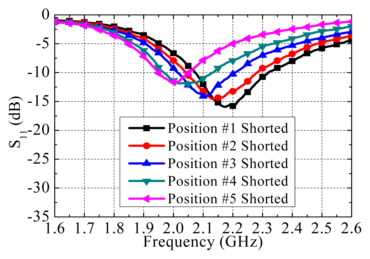
Fig. 4 shows the FTPIFAŌĆÖs S1, which was measured from the short-circuit operation of short positions #1 to #5 to verify changes in the resonant frequency of the antenna. Also Fig. 4 indicates that the resonant frequency decreased as the short position moved from #1 to #5 and that the central frequency (2.1 GHz) was determined when switch #3 was shorted. Because of the extent of the electric field, the magnetic energy between the antenna and the ground plane was changed by the short-circuit operation and on the basis of the perturbation principle [3]. In other words, the resonant frequency increased because of the reduction in the volume of the magnetic field energy near the feeding point when position #1 was shorted. Conversely, the resonant frequency decreased because of the reduction in the volume of the electric field energy at the edge of the radiated element when position #5 was shorted.
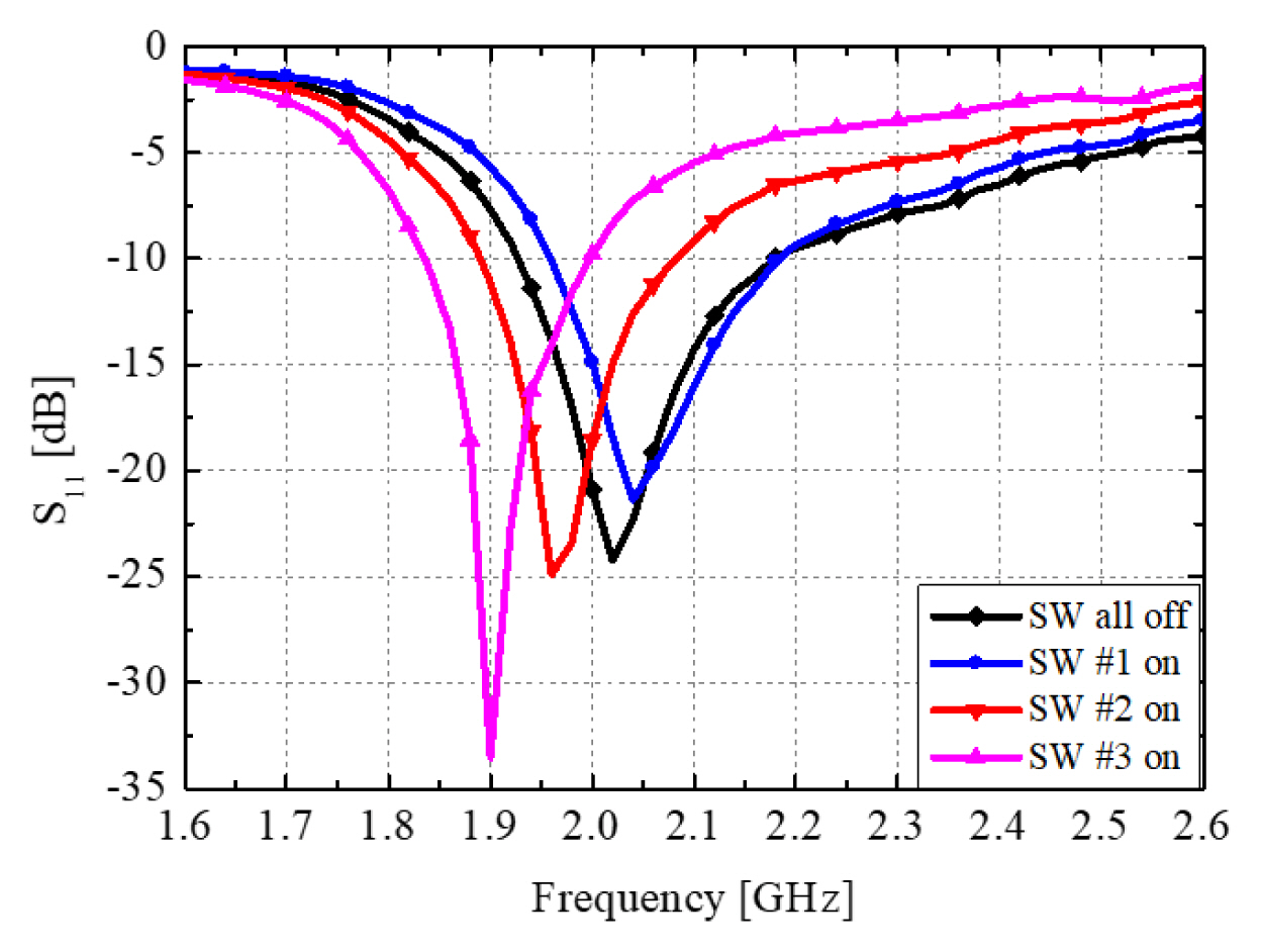
The electrical operation of the shorted position was realized by applying a DC bias to the PIN diodes. An inductor (22 nH) for AC cut-off and a meandered gap on the parasitic element for the independent operation of a switch were also used. Fig. 5 shows the S1 measured from the operation of switches #1 to #3, which were manipulated by turning a PIN diode on and off to determine changes in the antennaŌĆÖs resonant frequency. The number of switches was limited to three for equal intervals of frequency movement. When switch #1 was on, the upper frequency was resonant, but when switch #3 was on, the resonant frequency decreased given the change in the volume of the electric field energy. The measured ŌłÆ10 dB bandwidth covers 1.83 to 2.17 GHz, and the total tunable resonant frequency is 340 MHz (17.3%).
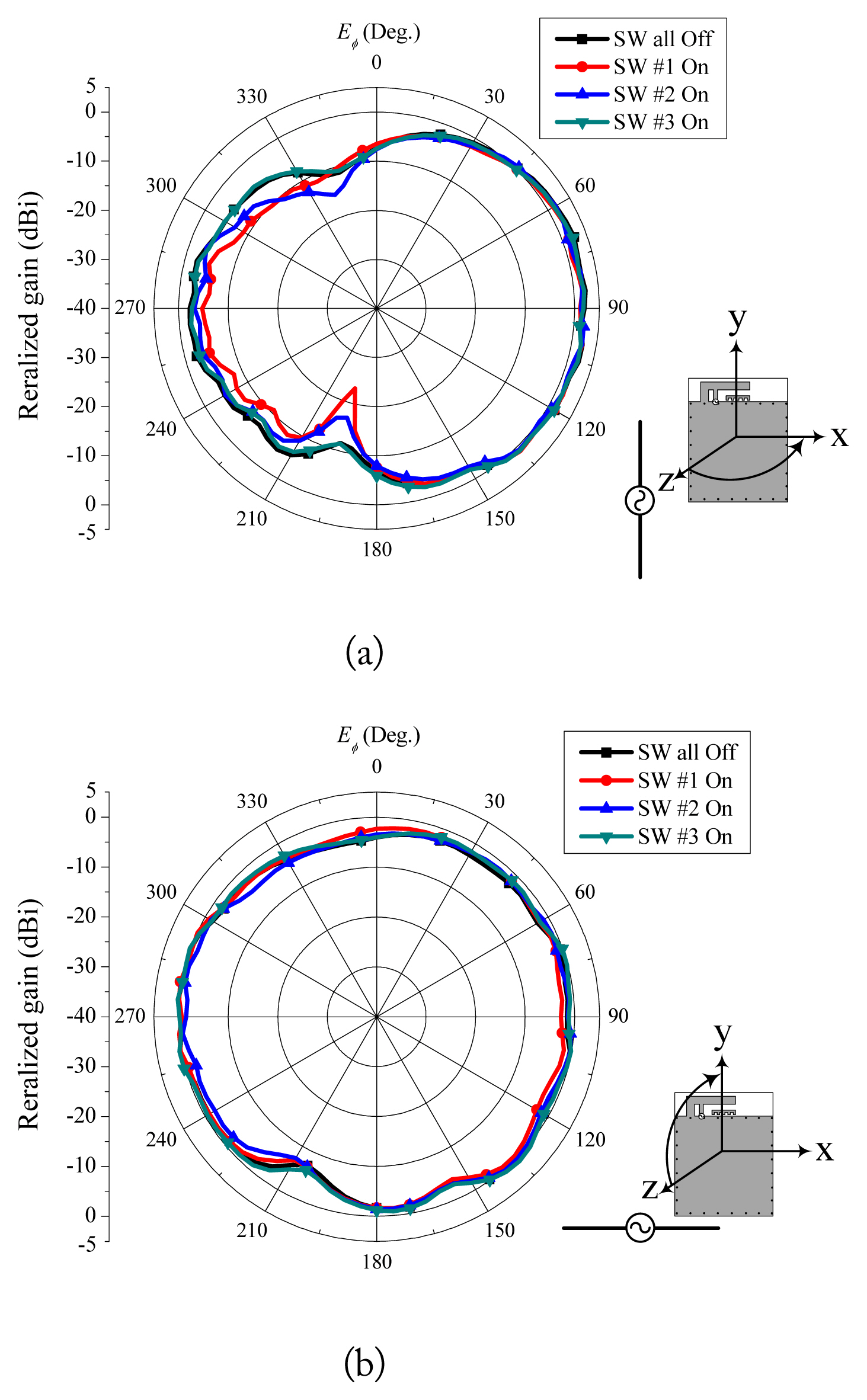
Fig. 6 shows the radiation patterns measured at each resonant frequency of the antenna prototype when the switches were on. The H-plane patterns of the vertical element that indicates directivity to the x-axis are shown in Fig. 6(a), and the H-plane patterns of the horizontal element overcoming a null point are displayed in Fig. 6(b). As can be seen, the designed antenna could maintain the radiation patterns of a basic inverted-F antenna, regardless of switch position.
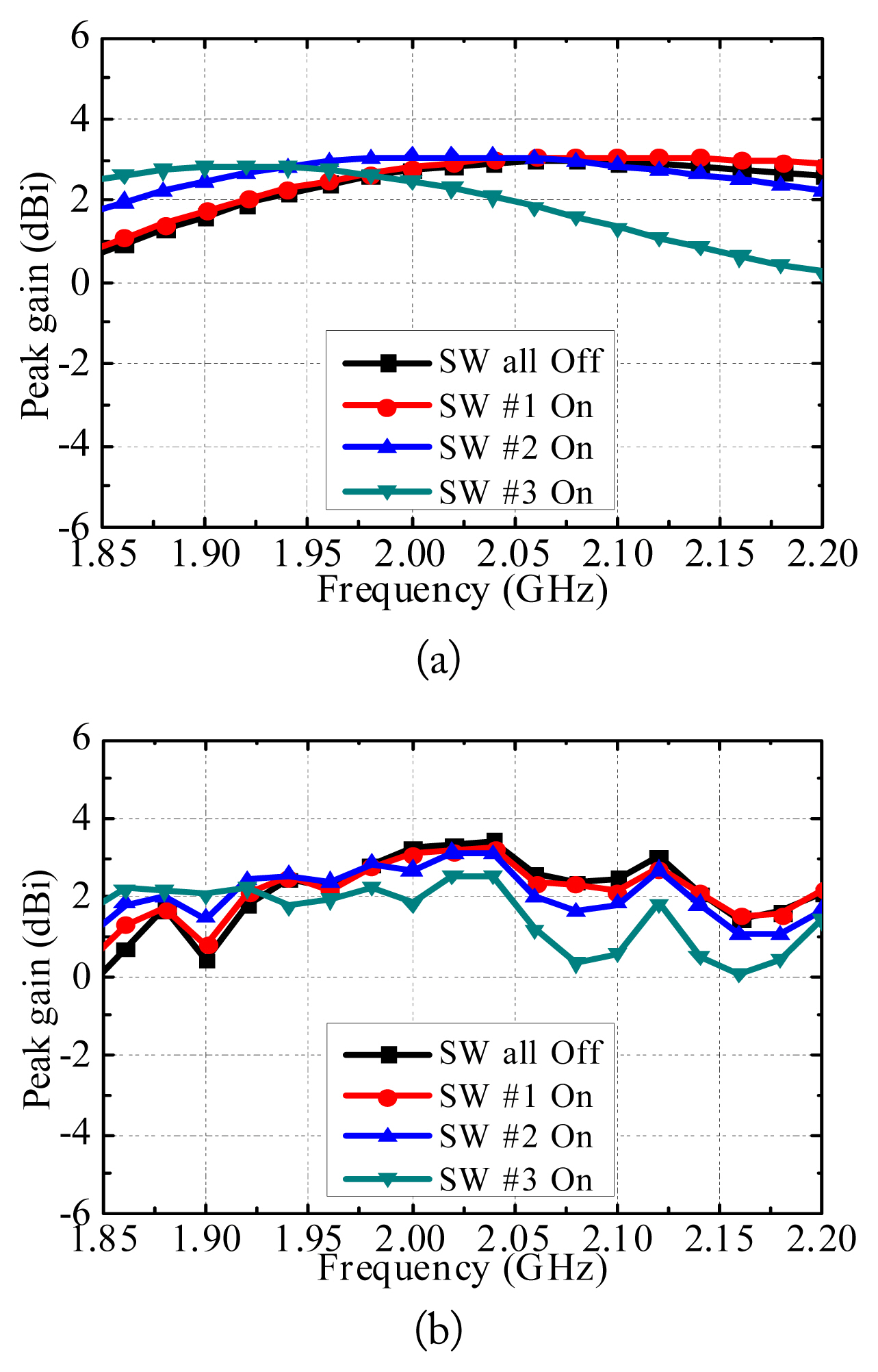
Fig. 7 shows the simulated and measured peak gains when each switch was on. The simulated and measured average realized gains were 3.0 dBi and 3.1 dBi, respectively, pointing to a reasonably good agreement between the simulation and measurement.
Finally, Table 1 summarizes the measured total efficiency and peak gain of the designed antenna at resonant frequencies. These amounted to 88.0% and 3.44 dBi at 2.02 GHz, respectively, when all the switches were off. When the switches were activated (switched on) sequentially, the measured total efficiency was 72.0% for switch #1, 68.9% for switch #2, and 56.2% for switch #3.
IV. Conclusion
An FTPIFA with a perturbed parasitic element was developed in this study. The designed antenna could be easily modified via the short- and open-circuit operation of the parasitic element between the antenna and the ground plane. It was redesigned by incorporating a gap capacitor into the parasitic element for the independent operation of each switch. As the resonant frequency varied considerably at the end of the radiator, a non-linear interval was arranged in the parasitic element. The antenna could also maintain the radiation patterns of a basic inverted-F antenna, regardless of switch position, and could be easily changed without loading and tuning the chip element on the antenna. Therefore, it is fully applicable to 5G technology and can selectively achieve the frequency band necessitated by an allocated frequency bandwidth.