I. Introduction
The power divider is a vital element in communication systems such as power amplifiers, mixers, and transceivers, owing to its simple design and superior performance. The conventional power divider has good matching of input and output, isolation performance, and low loss in narrow band operation. Due to its narrow band characteristics, its application has been limited in the current large-capacity communication systems of WCDMA, LTE, and 5G.
To address this limitation, a multi-section divider [1ŌĆō5] has been proposed. Although the multi-section divider has broadband characteristics with an achievable bandwidth greater than 100%, it has the disadvantages of a large circuit and increased insertion loss.
Recently, various designs to reduce the circuit size of power dividers have been researched, such as a structure using short uniform transmission line [6, 7], an isolation circuit positioned in a quarter-wavelength transformer [8, 9], and artificial transmission lines built up with lumped elements [10].
However, since these dividers use a ╬╗/4 transformer between the input and output or between the input or output and 50 ╬® termination, they cannot achieve an overall reduction in size. In addition, the bandwidth is reduced due to the impedance transformer, and the parasitic uncertainty of lumped elements is not desirable.
The power divider proposed in this paper has a multi-section structure to realize broadband characteristics, with the electrical length of each power splitting section less than a quarter wavelength to reduce the circuit size. The characteristic impedance of each power-splitting section can be controlled within a certain range while avoiding high impedance. All input and output ports are designed with 50 ╬® termination, so there is no need for an impedance transformer. In addition, a parallel resistorcapacitor circuit structure is adopted to obtain the broadband output matching and isolation characteristics of the proposed power divider.
II. Theory and Design
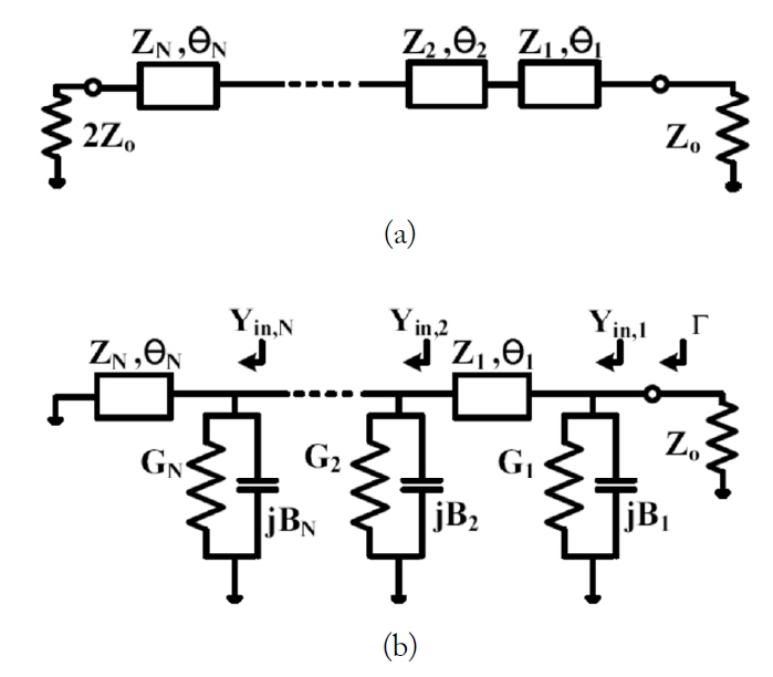
The structure of the proposed N-section power divider is shown in Fig. 1. It consists of transmission lines with electrical lengths (╬Ė
1, ╬Ė
2, ŌĆ” , ╬Ė
N
) less than 90┬░ and isolation circuits with parallel resistors (R
1, R
2, ŌĆ” , R
N
) and capacitors (C
1, C
2, ŌĆ” , C
N
). The proposed power divider is analyzed using the even-and odd-mode analysis methods; Fig. 2(a) and (b) show the even- and odd-mode equivalent circuits, respectively.
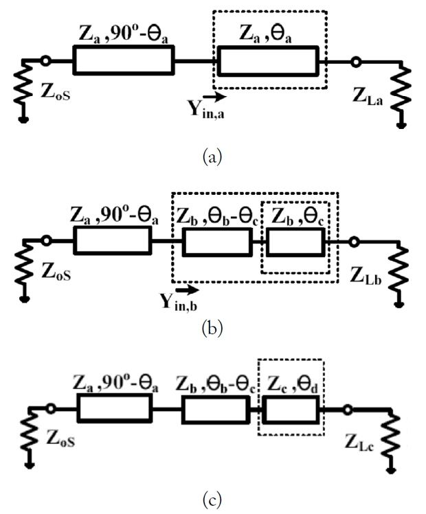
To obtain the electrical lengths and characteristic impedances of the transmission lines, the matching mechanism of the cascade transmission lines [11] is presented in Fig. 3. As seen in Fig. 3(a) and (b), it is possible to convert a part of the impedance transformer with Z
a
and 90┬░ to another impedance Z
b
and electrical length ╬Ė
b
. To match the conversion portion of the impedance transformer, the admittance values of Y
in,a
and Y
in,b
must be the same. By solving the equation for the real and imaginary parts of the admittance (Y
in,a
, Y
in,b
), the impedance Z
b
and terminating impedance Z
Lb
of the proposed two-section transformer for ╬Ė
b
change can be obtained as:
where
Ahn [12] confirmed that when the electrical length (╬Ė
a
< ╬Ė
b
< 90┬░) and termination conditions (Z
La
< Z
oS
) are satisfied, Z
b
and Z
Lb
should satisfy Z
b
< Z
a
and Z
Lb
< Z
La
. Using the above conditions, the impedance Z
c
and electrical length ╬Ė
d
of the three-section transformer can be obtained in the same way, as seen in Fig. 3(c). Using this method, all the electrical lengths of the multi-section transmission line, which is the proposed divider with each section length less than ╬╗/4 wavelength, can be obtained.
In addition, for the odd-mode equivalent circuit shown in Fig. 2(b), the following equations can be obtained:
where
G N = 2 R N Y N = 1 Z N
The conductance (G
1, G
2, ŌĆ”, G
N
) and susceptance (B
1, B
2, ŌĆ”, B
N
) values can be obtained to satisfy the condition that the reflection coefficient of Eq. (5) becomes zero.
To achieve isolation performance between ports 2 and 3, the S-parameter S
32 should be minimized as shown in Fig. 4. To calculate the isolation characteristic of the divider network, ABCD and admittance parameters are used. The ABCD matrix of the circuit Net
N
, which is composed of two transmission lines (Z
N
, ╬Ė
N
) and a shunt resistor Z
o
, can be expressed as:
(6)
The admittance matrix of the composite network Net
RCN
resistor-capacitor can be represented by:
Since the network Net
N
is connected in parallel with network Net
RCN
, we needed to transform Eq. (6) from an ABCD matrix to an admittance matrix. Finally, the composite admittance matrix of Net
N
and Net
RCN
can be obtained as follows:
To obtain the equation of the networks, which are connected by two cascade transmission lines (Z
N-
1, ╬Ė
N-
1) and the composite network of Net
N
and Net
RCN
, the composite network parameters are needed to convert the ABCD matrix. We can compute the ABCD parameters of the networks Net
N-
1 and Net
RCN-
1 as previously calculated. Through this process, the admittance parameters of the entire network can be obtained. The S-parameter value of isolation, S
32, is finally obtained by parameter conversion, and the isolation circuit values of the resistor and capacitor are selected to satisfy the S
32 parameter condition of |S
32| Ōēż ŌłÆ25 dB at the same time among the values satisfying Eq. (5).
III. Simulation and Experimental Results
To confirm the validation of the design rule, we designed two- and three-section power dividers operating at a frequency of 2 GHz and implemented on the substrate of Rogers RO4350B PCB (╔ø
r
= 3.48 and h = 0.762 mm). The simulation was performed using the Microwave Office software developed by National Instruments.
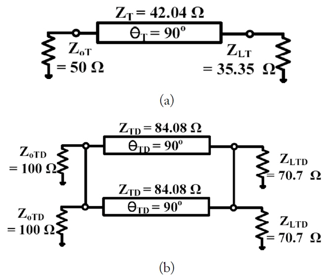
The two-section power divider configuration process is summarized as follows. First ╬╗/4 impedance transformer of Z
oT
= 50 ╬®, Z
LT
= 35.35 ╬®, Z
T
= 42.04 ╬® and ╬Ė
T
= 90┬░ is chosen as shown in Fig. 5(a).
Based on the decomposition theory of a single transmission line [13], the impedance transformer can be divided into two transmission lines of Z
oTD
= 100 ╬®, Z
LTD
= 70.7 ╬®, Z
TD
= 84.08 ╬®, and ╬Ė
TD
= 90┬░, as shown in Fig. 5(b). To constitute the two-section transmission line of the divider, the following parameters are set: Z
a
= 84.1 ╬® and ╬Ė
a
= 60┬░. The parameters of Z
b
= 69.56 ╬®, Z
Lb
= 50 ╬®, and ╬Ė
b
= 76┬░ can be calculated using Eqs. (1) and (2). To obtain the parameter values for the three-section lines, we used a similar method as follows:
The following parameters are set: Z
a
= 84.1 ╬® and ╬Ė
a
= 50┬░. The three-section parameters of Z
b
= 74.44 ╬®, Z
Lb
= 59.22 ╬®, ╬Ė
b
= 66┬░, Z
c
= 67.60 ╬®, Z
Lc
= 50 ╬®, and ╬Ė
d
= 73┬░ can be calculated as described previously. Finally, the resistor-capacitor values satisfying the reflection and isolation characteristics of the output ports are obtained using MATLAB and summarized as follows: In the case of the two-section divider, R
1
= 120 ╬®, C
1 = 0.02 pF, R
2 = 110 ╬®, and C
2 = 0.18 pF. In the case of the three-section divider, R
1 = 820 ╬®, C
1 = 0.01 pF, R
2 = 180 ╬®, C
2
= 0.02 pF, R
3 = 150 ╬®, and C
3 = 0.17 pF.
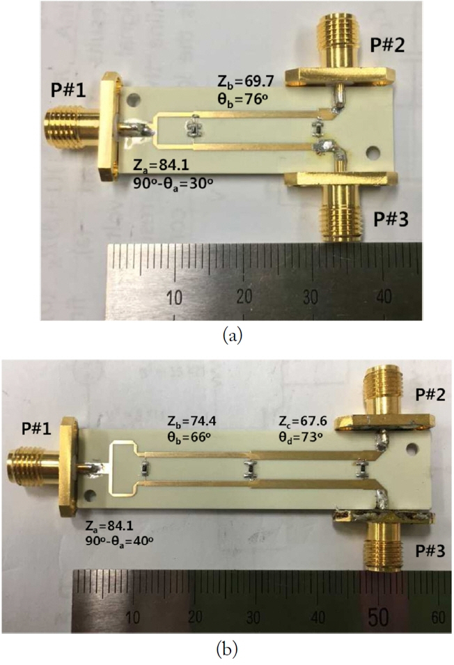
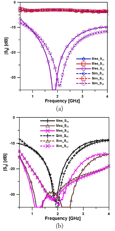
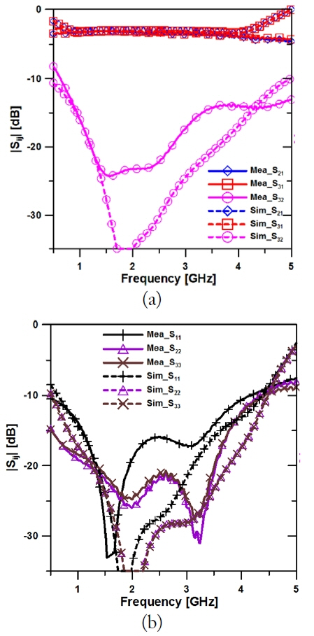
Fig. 6(a) and (b) show photographs of the two- and three-section proposed power dividers. The total length of the two-section divider is 106┬░, and that of the three-section divider is 179┬░. Fig. 7(a) and (b) show the measured and simulated S-parameters of the two-section power divider. The insertion losses of |S
21| and |S
31| were ŌłÆ3.10 dB, and the isolation of |S
32| was greater than 25 dB. The input return loss of |S
11| was better than ŌłÆ25 dB, and the output return losses of |S
22| and, |S
33| were better than ŌłÆ30 dB at the center frequency of 2 GHz. The measured ŌłÆ15 dB bandwidths of |S
11|, |S
22|, |S
33|, and |S
32| were in the ranges of 1.33ŌĆō2.46 GHz, 0.5ŌĆō3.63 GHz, 0.5ŌĆō3.35 GHz, and 1.26ŌĆō2.6 GHz, featuring fractional bandwidths of 56.5%, 156%, 142%, and 67%. In addition, Fig. 8(a) and (b) show the measured and simulated S-parameters of the three-section power divider. The insertion losses of |S
21| and |S
31| were ŌłÆ3.20 dB, and the isolation of |S
32| was greater than 22 dB. The input return loss of |S
11| was better than ŌłÆ19 dB, and output return losses of |S
22| and, |S
33
| were better than ŌłÆ24 dB at center frequency of 2 GHz. The measured ŌłÆ15 dB bandwidth of |S
11|, |S
22|, |S
33|, and |S
32| were in the ranges of 1.1ŌĆō3.42 GHz, 0.54ŌĆō3.76 GHz, 0.52ŌĆō3.76 GHz, and 0.95ŌĆō3.29 GHz, featuring fractional bandwidths of 116%, 161%, 162%, and 117%. Fig. 9 shows that the phase difference between the output ports in the two- and three-section power dividers was measured within ┬▒2.5┬░. Table 1 shows a comparison of the proposed divider with conventional multi-section divider.
IV. Conclusion
This paper presents a multi-section power divider with a parallel RC isolation circuit. Because each section of the power divider is less than ╬╗/4 wavelength, the power divider is implemented in a reduced size. In addition, the bandwidth of the matching and isolation characteristic showed that a fractional bandwidth above 100% is achievable in the three-section divider. By choosing the proper source and load impedance, the power divider can be implemented while avoiding the use of high impedance. By adopting decomposition and the improved transformer, the proposed power divider was demonstrated good performance, and the simulated and measured results were confirmed to be in good agreement.


