J. Electromagn. Eng. Sci Search

CLOSE


J. Electromagn. Eng. Sci > Volume 19(2); 2019 > Article
Yoon and Yoon: Bandwidth Enhancement of Single-Layer Microstrip Reflectarrays with Multi-Dipole Elements

Abstract

The gain bandwidth limit of a single-layer microstrip reflectarray is analyzed using multi-dipole elements. By observing the reflection phase characteristics of the multi-dipole elements with different numbers of dipoles, it is shown how the bandwidth can be enhanced by increasing the number of element resonant structures. The fundamental limit of the bandwidth enhancement is then derived by analyzing the coupling between the surface wave and the incident plane wave. It is shown that the surface wave can be excited even with the plane wave of normal incidence on the reflectarray and that the excitation frequency of the surface wave is dominated by array parameters and is almost independent of the number of resonant structures. The degradation of the element reflection characteristics caused by the surface wave, which limits the reflectarray bandwidth, is investigated. By comparing the radiation characteristics of three reflectarrays with three-, five-, and seven-dipole element, respectively, the analysis of the bandwidth enhancement and its limit is verified. The measured 1-dB gain bandwidth of the three-dipole element reflectarray is 25.12%, and the bandwidth is enhanced to 33.52% with the five-dipole element. However, because of the surface wave, no further bandwidth enhancement is achieved when the seven-dipole element is used, as predicted.

I. Introduction

A microstrip reflectarray is a planar reflector antenna with an array of reflective elements. The elements are designed to provide required reflection phase distributions over the surface of the reflectarray so that the desired radiation (reflection) patterns are achieved. Although a microstrip reflectarray has several advantages over a parabolic reflector antenna, such as a more compact (low-profile) size and an easier fabrication process, the gain bandwidth of the reflectarray is much narrower than that of the parabolic reflector. Such narrow bandwidth is mainly caused by the narrowband characteristics of the microstrip elements [1].
For broadband reflectarray design, the reflectarray elements should provide linear reflection phase curves (against the element dimensions change, such as the length of dipoles or the size of patches) that are parallel to each other at different frequencies [26]. If the phase curves are highly nonlinear, the reflection phases at different frequencies can easily converge at certain dimensions of the element, which is not desirable for broadband reflectarrays. In the case of a variable-sized rectangular patch element (one of the most commonly used element types), the reflection phase changes very sensitively to frequency variations near its resonance but is nearly independent of the frequency variations far from the resonance [7]. As a result, the bandwidth of the reflectarray with a variable-sized patch element is very narrow (typically 3%–5%) [1].
Therefore, there have been various researches on reflectarray elements to enhance the bandwidth of the microstrip reflectarray by improving the reflection phase characteristics of the elements. In [7, 8], multi-layer patch elements that control the reflection phase curve by adjusting relative dimensions of the patches on each layer are presented. However, multi-layer elements require high fabrication and material costs. Thus, bandwidth enhancement has been studied with single-layer structures and various single-layer elements that enhance the bandwidth by using multi-resonant structures have been proposed [26, 912]. Although various multiresonant elements with diverse shapes have been proposed, the basic operating mechanisms or design processes of the elements are similar: the dimensions of each resonant structure are adjusted so that each resonant frequency is shifted to achieve linear and parallel phase curves. In general, broader bandwidth can be achieved with larger numbers of resonant structures, as long as those structures can be adjusted appropriately.
The purpose of this paper is to answer the following question: Is it possible to continue enhancing the bandwidth by continuously increasing the number of resonant structures? Most previous studies on broadband microstrip reflectarrays have focused on achieving bandwidth enhancement, but few studies have reported on either the bandwidth enhancement mechanisms or the enhancement limit. In this paper, both the bandwidth enhancement and its limit for single-layer microstrip reflectarrays are analyzed using examples of multiresonant elements composed of parallel dipoles [4, 5] that are chosen because of their simple shapes. In this work, CST Microwave Studio is used to obtain full wave simulation results.

II. Bandwidth Enhancement of Single-Layer Microstrip Reflectarray Elements

As previously mentioned, the bandwidth enhancement of single-layer microstrip reflectarrays is generally achieved using multi-resonant type elements. In this section, it is shown that how the bandwidth can be enhanced by increasing the number of resonant structures of the multi-resonant elements. Specifically, multi-dipole elements are designed with an increased number of dipoles, and their reflection phase characteristics are analyzed.

1. Element Configuration

Fig. 1 shows the multi-dipole elements with single-, three-, and five-dipoles. The elements are symmetric with respect to the axis of the longest dipole at the center. The multi-dipole elements are designed on a substrate with a thickness of h = 3.175 mm, relative permittivity of ɛ r = 2.2, and loss tangent of tanδ = 0.0009. The element spacing is fixed at p = 10 mm (0.5 λ 0 at f 0 = 15 GHz). The lengths of the side dipoles l 1 and l 2 are proportional to the length of the center dipole l 0 with ratios r 1 and r 2, respectively (i.e., l 1 = r 1 × l 0 and l 2 = r 2 × l 0). The gap distance between the center dipole and the second dipoles is g 1, and the gap distance between the second dipole and the third dipole is g 2. The widths of the center dipole, the second dipole, and the third dipole are w 0, w 1, and w 2, respectively.

2. Bandwidth Enhancement

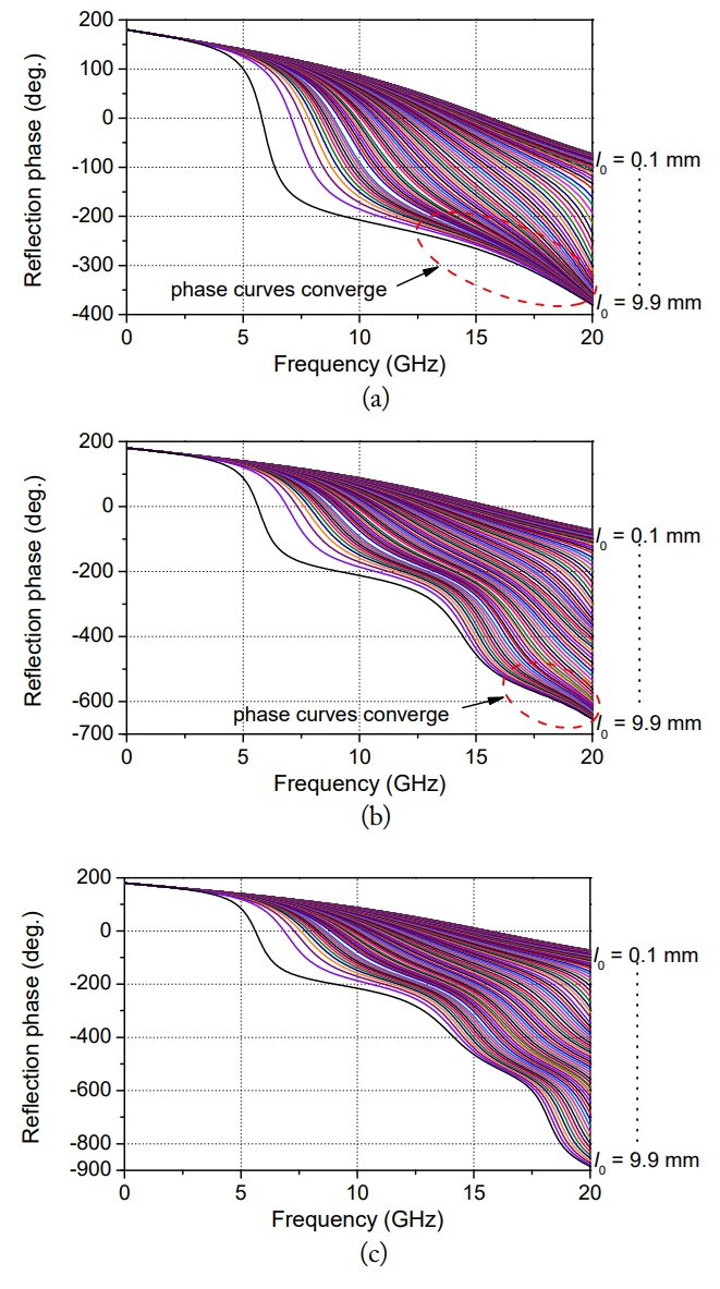
The single-dipole element shown in Fig. 1(a) is a singleresonant structure. The number of resonance increases as the number of side dipoles increases. Therefore, the three- and five-dipole elements in Fig. 1(b) and (c) are dual- and tripleresonant structures, respectively (detailed analysis of the resonance mechanism of the multi-dipole element can be found in [5]). Fig. 2 shows reflection phase curves of the multi-dipole elements when l 0 increases from 0.1 to 9.9 mm in 0.1 mm steps. The reflection phases were calculated under the assumption of infinite array of an identical element, which can be done by using plane wave of normal incidence on a single element in a waveguide composed of electric and magnetic walls [1]. The widths of the dipoles are w 0 = w 1 = w 2 = 0.5 mm, and the gaps between the dipoles are g 1 = g 2 = 0.5 mm. The ratios between the dipole lengths are designed as follows: r 1 = 0.65 and r 2 = 0.5 for both of the three- and five-dipole elements. These dimensions of the elements are chosen based on various parametric studies so that the phase curves of the elements become linear and parallel within the maximally achievable frequency range.
From Fig. 2, it is observed that the achievable phase delay increases as l 0 increases. In the case of the single-dipole element, the first resonance frequency (when the reflection phase is 0°) decreases as l 0 increases. However, the reflection phase curves begin to converge before the reflection phase exceeds −360° (the second resonance), as indicated by the dashed red circle in Fig. 2(a). Such convergence of phase curves is not desirable for broadband reflectarray design because the desired reflection phase distribution cannot be obtained.
As shown in Fig. 2(b) and (c), it is possible to achieve continuously spreading reflection phase curves with frequency by adding additional resonant structures. The second dipole of the three-dipole element induces the second resonance, and the phase delay can be increased to be larger than 360°. By adjusting r 1, the distance between the first and second resonant frequencies can be controlled so that highly nonlinear change of the reflection phase is avoided. However, the phase curves still converge before the reflection phase exceeds −720° (the third resonance), as indicated by the dashed red circle in Fig. 2(b). Since the phase curves begin to converge when f is larger than approximately 17 GHz, it is expected that the gain will begin to decrease as the frequency exceeds 17 GHz. Introducing the third dipole, the phase curves of the five-dipole element can continuously spread up to 20 GHz, as shown in Fig. 2(c).
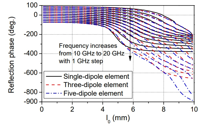
Fig. 3 shows the reflection phases against l 0 at various frequencies for the multi-dipole elements shown in Fig. 1. In the case of the single-dipole element, not only is the reflection phase range not wide enough to cover 360°, but also the phase curves are parallel to each other only in a narrow frequency range. In the case of the three-dipole element, the phase range is widened due to the increased number of resonances, and the phase curves are linear and parallel to each other in a wider frequency range when l 0 is larger than 5.5 mm, which is achieved by adjusting the dimensions of the dipoles. However, the slope of the phase curves is still reduced at upper frequencies (f > 17 GHz), as expected from Fig. 2(b). In the case of the five-dipole element, the phase curves are almost linear and parallel to each other from 10 to 20 GHz.

III. Limit of the Bandwidth Enhancement

In Section II, it was shown how the reflection phase characteristics desired for broadband reflectarray design can be achieved by increasing the number of resonant structures with single-layer elements.
Unfortunately, even though the number of resonant structures is continuously increased, the bandwidth enhancement of the reflectarray is limited due to the excitation of surface waves. The surface wave on the microstrip reflectarray can be excited if the propagation constant of the surface wave is matched to the transverse propagation constant of the incident plane wave. In this condition, the incident wave is coupled to the surface wave and dissipated as losses than reradiated with desired phase shift from the element. This phenomenon is similar to “scan blindness” in phased arrays [13, 14] where the incident wave in the blindness angle is not coupled to the array elements. The scan blindness is caused by the forced resonance of the surface wave. In microstrip reflectarrays, as incident wave is coupled to surface wave, the following two distinct phenomena occur (see Section III-2):
  1. The reduction of the reflection magnitude at the frequency of the surface wave coupling f sw .

  2. The distortion of the reflection phase at the frequencies close to f sw .

Similar phenomena were reported in [15, 16] but those studies were limited to a single-resonant element (a patch with variable size) and no study about the effect of the surface wave on the reflectarray bandwidth has been carried out. As will be shown in Section IV, both of these phenomena can severely degrade the efficiency of a reflectarray. In addition, as will be shown in Section III-1, the frequency of surface wave excitation f sw is almost independent from the element shape or the number of resonant structures but is dominated by array parameters, such as the element spacing and the thickness and permittivity of the substrate. Therefore, this surface wave excitation condition fundamentally limits the reflectarray bandwidth enhancement.

1. The Condition of Surface Wave Excitation

In phased arrays, because the element spacing is close to 0.5λ 0, the blindness angle is normally far from the bore-sight. In reflectarrays, however, the angles from a feeder to most elements are generally small. For instance, the maximum incident angle is only 26.5° for a reflectarray with F/D = 1 (where F is the distance from the feeder phase center to the center of the reflectarray and D is the diameter of the reflectarray) when the feeder is on the axis of the reflectarray. The angles to the dominant elements that are under relatively high levels of illuminated field from the feeder are close to 0°. Therefore, strong coupling between the surface wave and the incident wave (or forced resonance of the surface wave) does not occur.
However, when the element spacing of phased array is increased, the scan blindness can occur at an angle that is close to the bore-sight [17]. Similarly, the surface wave can be excited on a reflectarray even with the plane waves with small incident angles or, in extreme cases, with normal incidence as frequency increases. Because the surface wave mode that limits the bandwidth enhancement is the dominant mode with the lowest excitation frequency, in this work, f sw is considered for the TM0 mode only and can be derived using the relation between the grating lobe angle and the scan blindness angle, as follows.
With a planar array with element spacing p (= p x = p y ) on a dielectric substrate with thickness h and relative permittivity ɛ r , the grating lobe occurs at angle θ gr [18].
(1)
θgr=sin-1(2π/pk0-1).
The angle of scan blindness θ sb can then be calculated as follows:
(2)
θsb=θgr-sin-1(βswk0-1),
where β sw is the propagation constant of the TM0 surface wave on the unloaded grounded dielectric substrate. For a rigorous solution, β sw must be the propagation constant of the surface wave of the dielectric substrate with the printed elements. However, practically, this loading effect of the printed elements is small enough to be ignored and therefore β sw can be approximated by using the propagation constant of the unloaded dielectric substrate. The error of the blindness angle due to such approximation does not exceed a few tenths of a degree [14]. An approximate closed form of β sw is found in [19].
(3)
βsw2=k02[1+(ɛr-1)2ɛr2(k0h)2].
Finally, f sw under a normally incident plane wave can be derived with θ sb = 0, as follows:
(4)
fsw2=0.5[c0ɛr2πh(ɛr-1)]2[1+(4πh(ɛr-1)ɛrp)2-1],
where c 0 is the speed of light in free space. Note that f sw in Eq. (4) is dependent on the array parameters such as p, h, and ɛ r . In the following part of this section, it will be shown that f sw is almost independent from the shape of the element or the number of resonant structures but dominated by the array parameters by comparing the full wave simulation results with the analytic solutions.

2. Effects of the Surface Wave

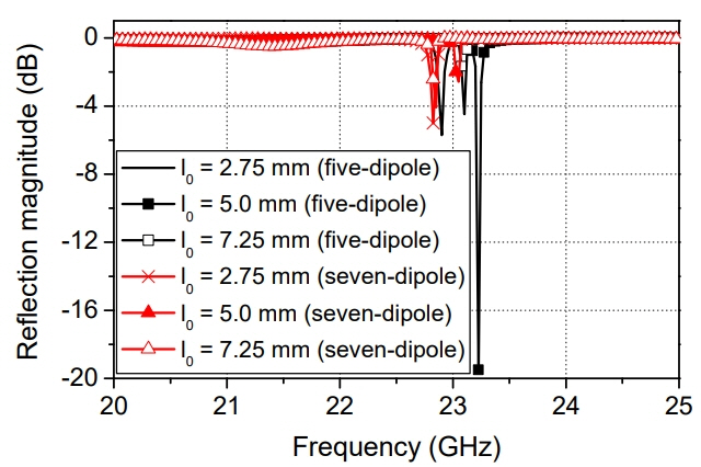
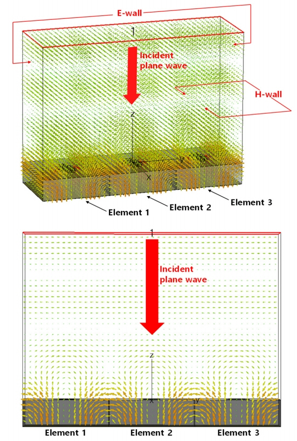
In the case of the multi-dipole elements in Section II (p = 10 mm, h = 3.175 mm, and ɛ r = 2.2), f sw is calculated as 23.03 GHz from (4). In Fig. 4, the magnitudes of the reflection coefficients of the five-dipole elements under plane wave of normal incidence are shown as black lines for different values of l 0. It is observed that the rapid reduction of the reflection magnitudes occurs near f sw = 23.03 GHz. The differences between f sw and actual frequencies of the surface wave excitation are due to the loading effect of the printed dipoles which are not considered in (4). When l 0 = 2.75 mm, the largest reduction of the magnitude occurs at 22.9 GHz. Fig. 5 shows electric field distribution excited by y-polarized plane wave of normal incidence on three identical five-dipole elements with l 0 = 2.75 mm at 22.9 GHz. The elements are placed inside a waveguide composed of electric and magnetic walls to assume an infinite array of the elements. Note that three identical elements (instead of one element) are shown in Fig. 5 only for better visualization of the surface wave. It is observed in Fig. 5 that the TM0 mode surface wave that is excited by the incident plane wave is propagating in the ydirection. Thus, most of the energy of the incident wave is excited as the surface wave, and the surface wave propagates until it is fully dissipated as dielectric and conductor losses. Such reduction of the reflected power significantly decreases the efficiency of the reflectarray.
In addition, the efficiency is degraded due to the convergence of the reflection phases near f sw , as in Fig. 6(a) that shows the reflection phases of the five-dipole element within the frequency range from 20 GHz to 25 GHz. The convergence of the phases occurs for the following reason. After the partial energy of the incident wave is coupled to the surface wave, the rest of the energy that is not coupled experiences the grounded dielectric substrate. Thus, the reflection phase at f sw becomes the same as the phase when a plane wave is normally incident on the grounded dielectric substrate (with no printed element pattern on the dielectric layer). As a result, assuming that the reflection phase of the grounded dielectric substrate is φ g , then the reflection phases near f sw converge to φ g –2πn (n = 0, 1, 2, …) as shown in Fig. 6(a).
Because f sw is almost independent from l 0, even if the number of dipoles is further increased, the bandwidth enhancement is still limited due to the surface wave. In Fig. 4, the reflection magnitudes of the seven-dipole element are shown as red lines. The seven-dipole element is designed by adding two shorter dipoles (with the length l 3 (= r 3 × l 0, r 3 = 0.3), the width w 3 = 0.5 mm, and the gap distance g 3 = 0.5 mm) to the five-dipole element. The reduction of the reflection magnitudes is also observed near f sw , as in the case of the five-dipole element. The reflection phases of the sevendipole element are shown in Fig. 6(b), where similar distortion (convergence) of the phase curves is also observed near f sw . Thus, it is obvious that the bandwidth enhancement of the reflectarray is limited due to the surface wave excitation, even with the increased number of dipoles.
It should be noted that similar phenomena are observed with the single- and three-dipole elements. In Table 1, the values of f sw extracted from full wave simulation are listed for the multi-dipole elements with different numbers of dipoles. They are designed with two different values of h and p, respectively. The values of f sw calculated using (4) are given in Table 1 for comparison. The maximum values of l 0 are 9.9 mm when p = 10 mm, and 14.9 mm when p = 15 mm, respectively. Because f sw shifts slightly as the shape or size of the printed element changes, as in Fig. 4, frequency ranges where the reflection magnitude reduction is larger than 3 dB are given for the values of f sw from the full wave simulation in Table 1. From Table 1, it is observed that the values of f sw from full wave simulation for various cases are close to f sw from (4) and not dominated by the element types. Therefore, it can be concluded that the bandwidth enhancement of a reflectarray with single-layer multi-resonant type elements is limited by the excitation of the surface wave, no matter how much the number of resonant structures is increased.

IV. Broadband Reflectarray Design

In this section, multi-dipole element reflectarrays with different number of dipoles are designed and analyzed to prove the bandwidth enhancement by increasing the number of resonant structures and its limit which has been discussed in previous sections.
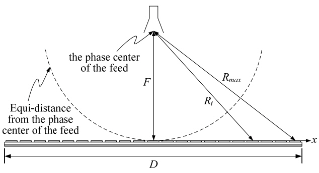
The configuration of the reflectarrays is shown in Fig. 7. In this work, three reflectarrays with identical dimensions are designed using the three-, five-, and seven-dipole elements, respectively, to compare the gain bandwidth (the single-dipole element reflectarray is not designed because it is well known that the gain bandwidth of the reflectarray is very narrow). The diameter of the reflectarrays is D = 300 mm (15λ 0 at f 0 = 15 GHz). The distance from the feeder phase center to the center of the reflectarrays is F = 426 mm (21.3λ0 at f 0 = 15 GHz), and the feeder is located on the axis of the reflectarray surface. Taconic TLY-5 substrates (ɛ r = 2.2, tanδ = 0.0009) with h = 3.175 mm are used as the substrates for the reflectarrays.
The reflectarrays are designed to obtain a main beam at the bore-sight, and for the reflectarray configuration of Fig. 7, the required reflection phase φ r of the i th element at the position x = x i is
(5)
φr(x,f)|x=xi=-2πfc0(Rmax-Ri(x))±2nπ+Δφ(f),
where R i is the distance from the phase center of the feeder to the i th element, R max is the distance from the phase center to the edge element, and Δφ is a phase offset that can be arbitrarily added to the reflection phase. Note that Δφ is a function of frequency. Theoretically, the phase offset Δφ can be changed with frequency without affecting the radiation characteristics of a reflectarray because Δφ is not a function of x i .
Although optimization techniques can be applied to broadband reflectarray design [2, 8, 10], no such optimization is used for the design of the reflectarrays in this work, i.e., the reflectarrays are designed to achieve the required phase distributions from (5) only at a single design frequency f 0 = 15 GHz (which is a conventional reflectarray design method). In this way, the bandwidth enhancement that only corresponds to the element change can be observed. For instance, it is expected that the single-dipole element reflectarray will have the narrowest gain bandwidth among the four reflectarrays because the linearity of the phase curves in Fig. 3 are rapidly reduced as frequency increases from f 0. In addition, it is expected that the gain at f 0 will be lowest because the achievable phase range at f 0 is less than 360°. The gains at f 0 and upper frequencies will be enhanced by using the three-dipole element, as the phase range at f 0 is larger than 360° and the linearity of the phase curves in Fig. 3 are well conserved until f = 17 GHz. The bandwidth enhancement up to f = 20 GHz will be achieved with the five-dipole element as the linearity of the phase curves are further improved, as shown in Fig. 3. The phase curves of the seven-dipole element are similar to those of the five-dipole element (not shown for brevity), and no further bandwidth enhancement will be achieved due to the surface wave excitation discussed in Section III.
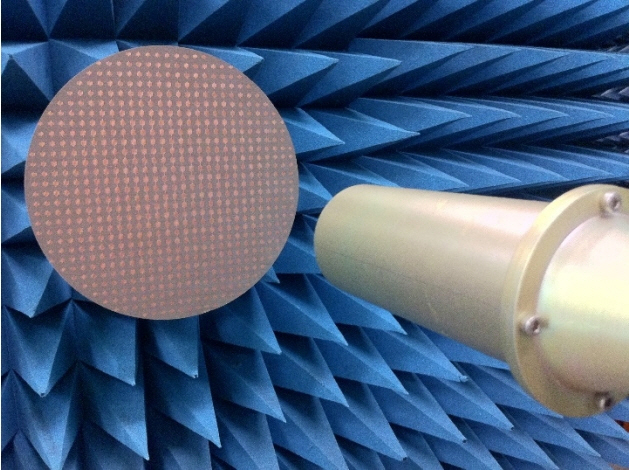
The three reflectarrays with the three-, five-, and seven-dipole elements were fabricated, and the five-dipole case is shown in Fig. 8 as an example. As a feeder for all three reflectarrays, a conventional circular dual-mode horn antenna presented in [20] was used.
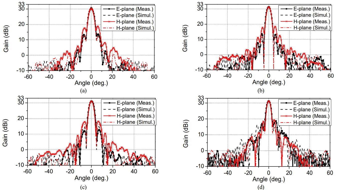
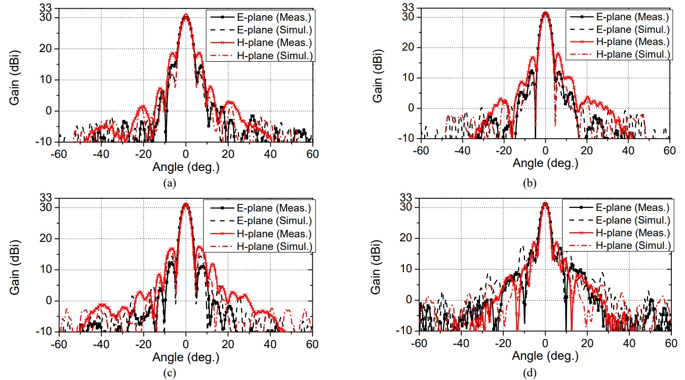
In Figs. 9 11, the radiation patterns of the three reflectarrays obtained from full wave simulation and measurement are shown at various frequencies. The measured peak gain of the three-dipole element reflectarrays at the design frequency f 0 = 15 GHz is G 0 = 31.0 dBi, and the corresponding aperture efficiency is η a = 59.1%. In the case of the five-dipole element reflectarray, G 0 = 31.4 dBi and η a = 64.1%. In the case of the seven-dipole element reflectarray, G 0 = 31.0 dBi and η a = 59.1%. The detailed radiation characteristics of the three reflectarrays at 15 GHz are summarized in Table 2.
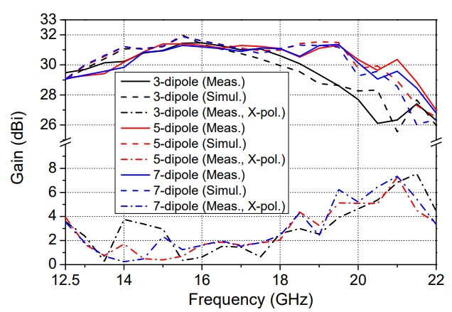
The gains against frequency are shown in Fig. 12. The lowest observation frequency is limited to 12.5 GHz due to the cut-off frequency of the feeder (a circular dual-mode horn antenna). The measured 1-dB gain bandwidth of the three-dipole element reflectarray is 25.12% (14.13–18.19 GHz). Meanwhile, the 1-dB gain bandwidths of the five-and seven-dipole element reflectarrays are 33.52% (14.13–19.82 GHz) and 33.11% (14.16–19.78 GHz), respectively. Thus, the gain bandwidth is enhanced by 33.42% and 31.84% by using the five- and seven-dipole elements, respectively. It is observed that the radiation patterns and gains of the three reflectarrays are similar at lower frequencies (f < 17 GHz), but the side lobe levels are increased and the gain is reduced as frequency increases in the case of the three-dipole element reflectarray, as expected. Also note that the gains of the seven-dipole element reflectarray are similar to those of the five-dipole element reflectarray for the entire frequency range of interest, and no further bandwidth enhancement is observed with the increased number of dipoles, as predicted.

V. Conclusion

In this paper, the bandwidth enhancement and limit of a single-layer microstrip reflectarray have been analyzed. First, by observing the reflection phase characteristics of the multi-dipole element with different numbers of dipoles, it has been shown how the bandwidth can be enhanced by increasing the number of the element resonant structures. Second, the limit of the bandwidth enhancement by increasing the number of resonant structures has been analyzed. It has been shown that the bandwidth is limited due to the excitation of the surface wave at the upper frequency which is dominated by the array parameters (such as the element spacing and the thickness of the substrate), rather than the shape of the resonant structures. The effects of the surface wave that reduces the reflection magnitude and distorts the reflection phase near the frequency of the surface wave excitation have been observed, which reduces the gain and, thus, limits the gain bandwidth.
The enhancement of the bandwidth and its limit has been proved by comparing the radiation characteristics of the three-, five-, and seven-dipole element reflectarrays. The three reflectarrays were designed with identical dimensions. Through full wave simulation and measurement, it has been shown that the gain bandwidth is enhanced by increasing the number of the dipoles from three to five. However, no further enhancement can be achieved, even though the number of dipoles is increased to seven due to the surface wave.
The analysis of the bandwidth limit is expected to give guidelines to broadband microstrip reflectarray designs. Although the analysis in this paper is limited to the case of single-layer microstrip reflectarrays, in the future, the study can be extended to the case of multi-layer reflectarrays.

Fig. 1
The elements with dipole resonators: (a) single-dipole element, (b) three-dipole element, and (c) five-dipole element.
jees-19-2-130f1.jpg
Fig. 2
The reflection phases of the multi-dipole elements against frequency: (a) single-dipole element, (b) three-dipole element, and (c) five-dipole element.
jees-19-2-130f2.jpg
Fig. 3
The reflection phase of the multi-dipole elements against l 0.
jees-19-2-130f3.jpg
Fig. 4
The reflection magnitude of the five- and seven-dipole elements.
jees-19-2-130f4.jpg
Fig. 5
The surface wave excited from plane wave of normal incidence on the five-dipole elements (l 0 = 2.75 mm) at f = 22.9 GHz.
jees-19-2-130f5.jpg
Fig. 6
The reflection phase of the five-dipole element (a) and seven-dipole element (b).
jees-19-2-130f6.jpg
Fig. 7
The configuration of the reflectarrays.
jees-19-2-130f7.jpg
Fig. 8
The fabricated reflectarray with the five-dipole element.
jees-19-2-130f8.jpg
Fig. 9
The radiation patterns of the three-dipole reflectarray: (a) 14.0 GHz, (b) 15.0 GHz, (c) 16.5 GHz, and (d) 19.5 GHz.
jees-19-2-130f9.jpg
Fig. 10
The radiation patterns of the five-dipole reflectarray: (a) 14.0 GHz, (b) 15.0 GHz, (c) 16.5 GHz, and (d) 19.5 GHz.
jees-19-2-130f10.jpg
Fig. 11
The radiation patterns of the seven-dipole reflectarray: (a) 14.0 GHz, (b) 15.0 GHz, (c) 16.5 GHz, and (d) 19.5 GHz.
jees-19-2-130f11.jpg
Fig. 12
The gains of the multi-dipole element reflectarrays against frequency.
jees-19-2-130f12.jpg
Table 1
Frequency of the surface wave excitation of the single-layer multi-resonant elements
h (mm) p (mm) Frequency of TM0 mode surface wave excitation, f sw (GHz)

From (4) 1 dipole 3 dipoles 5 dipoles
1.575 7 35.98 35.24–35.49 34.72–35.64 34.64–36.39
10 26.99 26.37–26.55 26.01–26.70 25.83–26.74
3.175 7 29.35 29.01–30.17 28.66–30.35 29.58–30.17
10 23.03 22.78–23.43 22.52–23.40 22.55–23.48
Table 2
The radiation characteristics of the multi-dipole reflectarrays at 15 GHz
Three-dipole reflectarray Five-dipole reflectarray Seven-dipole reflectarray


Simulation Measurement Simulation Measurement Simulation Measurement
Gain (dBi) 31.2 31.0 31.2 31.4 31.2 31.0
Aperture efficiency (%) 61.5 59.1 61.5 64.1 61.5 59.1
SLL (dB)
 E-plane −21.0 −17.1 (L), −22.7 (R) −22.1 −17.6 (L), −18.1 (R) −22.6 −19.0 (L), −19.5 (R)
 H-plane −19.2 −12.6 (L), −13.5 (R) −19.4 −13.4 (L), −12.8 (R) −19.7 −14.5 (L), −13.2 (R)
HPBW (°)
 E-plane 3.8 4.3 3.8 4.1 3.8 4.4
 H-plane 3.7 3.9 3.7 3.8 3.7 3.8

SLL = sidelobe level, HPBW = half power beamwidth.

References

1. J Huang and JA Encinar, Reflectarray Antennas. Hoboken, NJ: Wiley-IEEE Press, 2008.

2. QY Chen, SW Qu, JF Li, Q Chen, and MY Xia, "An X-band reflectarray with novel elements and enhanced bandwidth," IEEE Antennas and Wireless Propagation Letters, vol. 12, pp. 317–320, 2013.
crossref
3. QY Chen, SW Qu, XQ Zhang, and MY Xia, "Low-profile wideband reflectarray by novel elements with linear phase response," IEEE Antennas and Wireless Propagation Letters, vol. 11, pp. 1545–1547, 2012.
crossref
4. R Florencio, RR Boix, E Carrasco, JA Encinar, M Barba, and G Perez-Palomino, "Broadband reflectarrays made of cells with three coplanar parallel dipoles," Microwave and Optical Technology Letters, vol. 56, no. 3, pp. 748–753, 2014.
crossref
5. JH Yoon, YJ Yoon, WS Lee, and JH So, "Broadband microstrip reflectarray with five parallel dipole elements," IEEE Antennas and Wireless Propagation Letters, vol. 14, pp. 1109–1112, 2015.
crossref
6. A Vosoogh, K Keyghobad, A Khaleghi, and S Mansouri, "A high-efficiency Ku-band reflectarray antenna using single-layer multiresonance elements," IEEE Antennas and Wireless Propagation Letters, vol. 13, pp. 891–894, 2014.
crossref
7. JA Encinar, "Design of two-layer printed reflectarrays using patches of variable size," IEEE Transactions on Antennas and Propagation, vol. 49, no. 10, pp. 1403–1410, 2001.
crossref
8. J Encinar and JA Zornoza, "Broadband design of a three-layer printed reflectarray," IEEE Transactions on Antennas and Propagation, vol. 51, no. 7, pp. 1662–1664, 2003.
crossref
9. MR Chaharmir and J Shaker, "Broadband reflectarray with combination of cross and rectangle loop elements," Electronics Letters, vol. 44, no. 11, pp. 658–659, 2008.
crossref
10. MR Chaharmir, J Shaker, and H Legay, "Broadband design of a single layer large reflectarray using multi cross loop elements," IEEE Transactions on Antennas and Propagation, vol. 57, no. 10, pp. 3363–3366, 2009.
crossref
11. JH Yoon, JS Kim, YJ Yoon, WS Lee, and JH So, "Single-layer reflectarray with combination of element types," Electronics Letters, vol. 50, no. 8, pp. 574–576, 2014.
crossref
12. JH Yoon, YJ Yoon, WS Lee, and JH So, "Wband microstrip reflectarray with double-cross element for bandwidth improvement," In: Proceedings of Global Symposium on Millimeter-Waves (GSMM); Montreal, Canada. 2015, pp 1–3.
crossref
13. D Pozar and D Schaubert, "Scan blindness in infinite phased arrays of print diploes," IEEE Transactions on Antennas and Propagation, vol. 32, no. 6, pp. 602–610, 1984.
crossref
14. D Pozar and D Schaubert, "Analysis of an infinite array of rectangular microstrip patches with idealized probes feeds," IEEE Transactions on Antennas and Propagation, vol. 32, no. 10, pp. 1101–1107, 1984.
crossref
15. H Rajagopalan and Y Rahmat-Samii, "On the reflection characteristics of a reflectarray element with low-loss and high-loss substrates," IEEE Antennas and Propagation Magazine, vol. 52, no. 4, pp. 73–89, 2010.
crossref
16. KK Karnati, Y Yusuf, S Ebadi, and X Gong, "Theoretical analysis on reflection properties of reflectarray unit cells using quality factors," IEEE Transactions on Antennas and Propagation, vol. 61, no. 1, pp. 201–210, 2013.
crossref
17. AK Bhattacharyya, Phased Array Antennas: Floquet Analysis, Synthesis, BFNs and Active Array Systems. New York, NY: John Wiley & Sons, 2006.

18. PD Patel, "Approximate location of scan-blindness angle in printed phased arrays," IEEE Antennas and Propagation Magazine, vol. 34, no. 5, pp. 53–54, 1992.
crossref
19. DM Pozar, "Rigorous closed-form expressions, for the surface wave loss of printed antennas," Electronics Letters, vol. 26, no. 13, pp. 954–956, 1990.
crossref
20. JS Kim, JH Yoon, YJ Yoon, WS Lee, and CG Kim, "Design of modified dual mode horn antenna to improve E/H-plane radiation pattern symmetry," In: Proceedings of 2012 International Symposium on Antennas and Propagation (ISAP); Nagoya, Japan. 2012, pp 547–550.

Biography

Ji Hwan Yoon received a Ph.D. degree in Electrical and Electronic Engineering from Yonsei University, Seoul, Korea in 2016. Since March 2016, he has been with the Agency for Defense and Development, Korea, where he is currently a senior researcher. His research interests include airborne radar systems, phased array radars, and reflectarrays.
jees-19-2-130i1.jpg

Biography

Young Joong Yoon (M’93-SM’10) received B.S. and M.S. degrees in electronics engineering from Yonsei University, Seoul, Korea in 1981 and 1986, respectively, and a Ph.D. degree in electrical engineering from the Georgia Institute of Technology, Atlanta, GA, USA in 1991. He was a Senior Researcher with the Electronics and Telecommunications Research Institute, Daejeon, Korea from 1992 to 1993. He joined Yonsei University in 1993 as a Faculty Member, where he is currently a Professor with the Department of Electrical and Electronics Engineering. He was the President of the Korean Institute of Electromagnetic Engineering and Science, Seoul in 2012. His current research interests include high-power antennas, reflectarrays, hyperthermia systems, and array antennas.
jees-19-2-130i2.jpg
TOOLS
Share :
Facebook Twitter Linked In Google+
METRICS Graph View
  • 6 Crossref
  • 5 Scopus
  • 6,004 View
  • 153 Download
Related articles in JEES

ABOUT
ARTICLE CATEGORY

Browse all articles >

BROWSE ARTICLES
AUTHOR INFORMATION
Editorial Office
#706 Totoo Valley, 217 Saechang-ro, Yongsan-gu, Seoul 04376, Korea
Tel: +82-2-337-9666    Fax: +82-2-6390-7550    E-mail: admin-jees@kiees.or.kr                

Copyright © 2024 by The Korean Institute of Electromagnetic Engineering and Science.

Developed in M2PI

Close layer
prev next