Dual-Band Microstrip Patch Antenna with Switchable Orthogonal Linear Polarizations
Article information
Abstract
This study presents a dual-band polarization-reconfigurable antenna that comprises a large square patch with a pair of corner-cut edges and two small square patches with a shorting via. Two PIN diodes are located between the large square patch and two small square patches. Depending on the bias state applied to the two PIN diodes, each small patch may be disconnected or connected to the large square patch. As a result, the proposed antenna can provide polarization reconfigurability between two orthogonal linear polarizations. Further, the proposed antenna operates at 2.51 GHz and 2.71 GHz. From the measured results, the proposed antenna shows a 10 dB bandwidth of 2.39% (2.49–2.55 GHz) and 2.58% (2.68–2.75 GHz). In this work, the frequency ratio can be easily controlled by changing the size of the small patch.
I. Introduction
Polarized reconfigurable antennas have been extensively researched and adopted in multiple-input multiple-output (MIMO) systems because of their inherent polarization diversity advantages of mitigating multipath fading and increasing channel capacity [1]. The polarization characteristics of these antennas can be switched among linear polarization (LP), left circular polarization (LHCP), and right circular polarization (RHCP) depending on the propagation environment. However, most studies have been limited to polarization diversity between RHCP and LHCP [2–5]. In addition, the study on polarization diversity between orthogonal LPs is relatively inadequate [6–9].
A polarization diversity reconfigurable antenna with a switchable feed structure is proposed in [6]. By changing the operating state of four pairs of PIN diodes in the switchable feed network, the feed point of the circular patch antenna can be switched. Therefore, a reconfiguration between four linear polarization directions at a 45° interval (22.5°, 67.5°, 112.5°, and 157.5°) can be realized. Four shorting posts and four PIN diodes are placed at a 45° interval, and four PIN diodes control the connection between the shorting via the ground plane [7]. As a result, the antenna can switch between the four LPs at 45° intervals. The difference from [6] is that the RF switch is applied to the radiator rather than to the feed structure and uses a single-layer substrate. In [8], a reconfigurable slot antenna switching between vertical and horizontal LPs is proposed. To control the direction of the electric field formed in the feed structure, two PIN diodes are applied to the CPW-to-slot line switch. Consequently, two LPs perpendicular to each other are realized. In [9], a PIN diode is applied at the end of the feed line. By adjusting the state of the PIN diode, the impedance of the feed end can be electrically switched to a short or open. Therefore, the polarization state can be controlled between the two LPs.
As far as we know, only two studies have been published on polarization diversity between LPs in antennas operating in a dual band. In [10], the authors present a single-feed dual-band microstrip patch antenna with switchable orthogonal LPs. However, because the frequency ratio is greater than 2 and the difference in antenna performance at two resonant frequencies is too large, the proposed antenna can be used only in a limited area. In [11], a single-fed dual-band polarization-reconfigurable antenna is first proposed for wireless local area network (WLAN) applications. The two resonance modes of this antenna utilized the TM10 and TM30 modes, respectively, of the squarepatch antenna. However, as the TM30 mode has a higher order, a side lobe is largely generated on a radiation pattern at the second resonant frequency.
In this study, we present a simple microstrip patch antenna for switching two orthogonal LPs in a dual band. In the proposed antenna, a square patch with a cutting corner works as a radiating element, and two small square patches with a shorting via are used to control the direction of the polarization. As the PIN diode is turned on/off, the square patch and the small patch are connected/disconnected, respectively. As a result, the electrical length of the antenna is changed along with the resonant frequency. The details of the proposed antenna design and the simulated and measured results are described as follows.
II. Antenna Geometry
Fig. 1 shows the geometry of the proposed antenna. The proposed antenna uses FR-4 with relative permittivity of ɛr = 4.4, at a thickness of h = 1.6 mm. In the proposed structure, a large square patch with a side length L1 acts as a radiator. Two small square patches with a side length L2 have a shorting via of diameter R in the middle of the patch. Some of the large square patches are cut out to make room for the small patches. As a diode (HSMP-3860) is applied between the large square and the small square, the gap distance between them is set to g. The position of the via or the gap determines the polarization direction of the square patch [13]. Large and small patches are connected or disconnected depending on the state of the diode. When connected, the polarization direction of the large patch changes because of the influence of the via. As the via is located on the left and right diagonal lines of the large patch, we can connect the two vias alternately to the large patch to create two polarizations perpendicular to each other. The bias voltage of the PIN diode is 0.75 V. The PIN diodes have a resistance of 1.5 Ω in the forward-bias state and a capacitance of 0.2 pF in the reverse-bias state. For the simulation, the equivalent circuit of the PIN diode is represented by a resistor of 1.5 Ω in the forward bias state. Conversely, in the reverse bias state, the equivalent circuit of the PIN diode is represented by a capacitor of 0.2 pF.
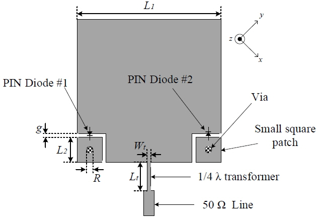
Geometry of proposed reconfigurable antenna for a dual-band operation. The figure is not drawn to scale.
The bias tee is used in this study to measure the proposed antenna. State I is defined as the condition when PIN diode #1 is in the on-state and PIN diode #2 is in the off state; that is, a positive voltage is applied to the feed line through the bias tee, and a negative voltage is applied to the ground plane. Further, State II is defined as the condition when PIN diode #1 is in the off-state and PIN diode #2 is in the on state; that is, a positive voltage is applied to the ground plane, and a negative voltage is applied to the feed line through the bias tee.
III. Simulated and Measured Results
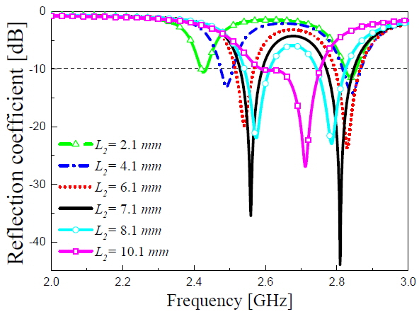
Fig. 2 shows the simulated reflection coefficients of the proposed antenna relative to the change in L2. The other parameters are as follows: L1 = 28 mm, R = 0.5 mm, g = 0.5 mm, Wt = 0.72 mm, and Lt = 20.2 mm. In the proposed structure, the gap g between the large patch and the small patch is not suitable as a variable for the parameter study because the diode should be applied. The gap g is fixed to 0.5 mm considering the size of the PIN diode. Therefore, when the side length L2 of the small square patch increases, the size of the cut part at the two corners of the large patch increases. As L2 increases, the first resonant frequency increases, and the second resonant frequency decreases. The frequency ratio (f2 / f1) changes to 1.15 when L2 = 2.1 mm. If L2 is smaller than 2.1 mm, the frequency ratio becomes larger, but the matching property deteriorates (|S11| > −10 dB). If L2 is larger than 10.1 mm, the two resonant frequencies approach each other and operate as a single-band antenna with a wide bandwidth. As will be mentioned later, the polarization at two resonant frequencies is perpendicular to each other. Therefore, if L2 is larger than 10.1 mm, a CP antenna is realized. L2 is selected to be 7.1 mm in consideration of optimized matching. If L2 is larger than 7.1 mm, the matching characteristics at two resonant frequencies are degraded.
Fig. 3 shows the simulated reflection coefficient of the proposed antenna with respect to radius R. The remaining parameters are the same as those mentioned above. In this case, diode #1 is on and diode #2 is off. As R increases, the first resonant frequency f1 changes little and the second resonant frequency f2 increases, and the impedance matching characteristic is insensitive to the changes in the radius. In Fig. 1, R = 0 mm denotes the antenna without the via. The antenna with R = 0 mm exhibits a single resonance at 2.57 GHz. Based on this fact, the second resonant frequency of the proposed antenna is generated by the via. In [12], the shorting pin is applied to the ring antenna, and the polarization at the dominant frequency is vertically changed by the shorting pin. In the current study, the polarization at the second resonant frequency generated by the shorting pin is perpendicular to the polarization at the first resonant frequency.
Fig. 4(a) shows the simulated field distribution when the proposed antenna operates in State I (diode #1 on, diode #2 off). The simulation is performed at the resonant frequencies of 2.56 GHz and 2.82 GHz. In the figure, the electric field is weak in the dark area and strong in the bright area. At the first resonant frequency of 2.56 GHz, the null line of the electric field is formed along the diagonal line ϕ = 90° including the via. At the second resonant frequency of 2.82 GHz, the null line of the electric field is formed along the perpendicular diagonal line ϕ = 0°. This diagonal line has no via. Fig. 4(b) shows the electric field distribution in the proposed antenna in State II. At the first resonant frequency, the null line of the electric field is formed perpendicular to the case of State I. As shown in Fig. 4, the two perpendicular LPs have a good isolation between them. Therefore, an antenna with two orthogonal polarizations at the same frequency is suitable for a polarization diversity application.
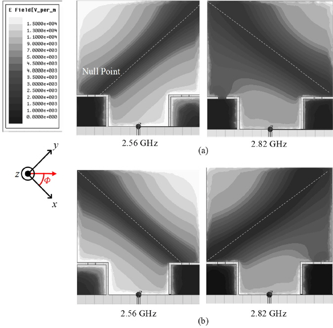
Simulated electric field distribution at 2.56 GHz (left) and 2.82 GHz (right). (a) State I and (b) State II.
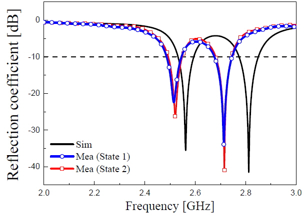
Fig. 5 shows the photograph of the fabricated antenna, and Fig. 6 illustrates the simulated and measured reflection coefficient of the proposed antenna. Ansoft’s High-Frequency Structure Simulator (HFSS) is used for the simulation. For the simulation and measurement, the designed parameters of the proposed antenna are L1 = 28 mm, L2 = 7.1 mm, R = 0.5 mm, g = 0.5 mm, Wt = 0.72 mm, and Lt = 20.2 mm. The measured antenna shows a 10 dB f1 bandwidth of 2.39% (2.49–2.55 GHz) and a 10 dB f2 bandwidth of 2.58% (2.68–2.75 GHz). As shown in the graph, a good agreement between the simulation and the measurement is achieved, with an error of less than 3.0 % in the predicted minimum reflection coefficient frequency. This small deviation is partially due to the diffracted field at the edge of the substrate. Moreover, although Bias-T is used, the resonant frequencies of the proposed antenna can be predicted to be slightly reduced because of the DC bias structure.
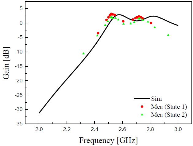
Fig. 7 shows the simulated and measured radiation patterns in the xz and yz planes at the two resonant frequencies of 2.51 GHz and 2.71 GHz. At this time, diode #1 is on and diode #2 is off. The measured results are in good agreement with the simulated results. The radiation pattern in the xz plane is tilted by 20° because of the via. As the radiation pattern of the proposed antenna has a wide beam width, the fact that the radiation pattern is tilted does not pose a problem because the gains at ϕ = 0° and ϕ = 20° are almost the same. Fig. 8 shows the simulated and measured radiation patterns at both resonant frequencies when diode #1 is off and diode #2 is on. As shown in Figs. 5 and 6, two polarizations are orthogonal to each other at the two resonant frequencies. Fig. 9 shows the simulated and measured total gains with regard to the frequency. The measured peak gain is 3.20 dBi at the operating frequency of 2.51 GHz. The measured peak gain is 2.37 dBi at the operating frequency of 2.71 GHz.

Simulated and measured radiation patterns of State I (diode #1 is on and diode #2 is off): (a) E-plane (yz plane) at 2.51 GHz, (b) H-plane (xz plane) at 2.51 GHz, (c) E-plane (yz plane) at 2.71 GHz, and (d) H-plane (xz plane) at 2.71 GHz.
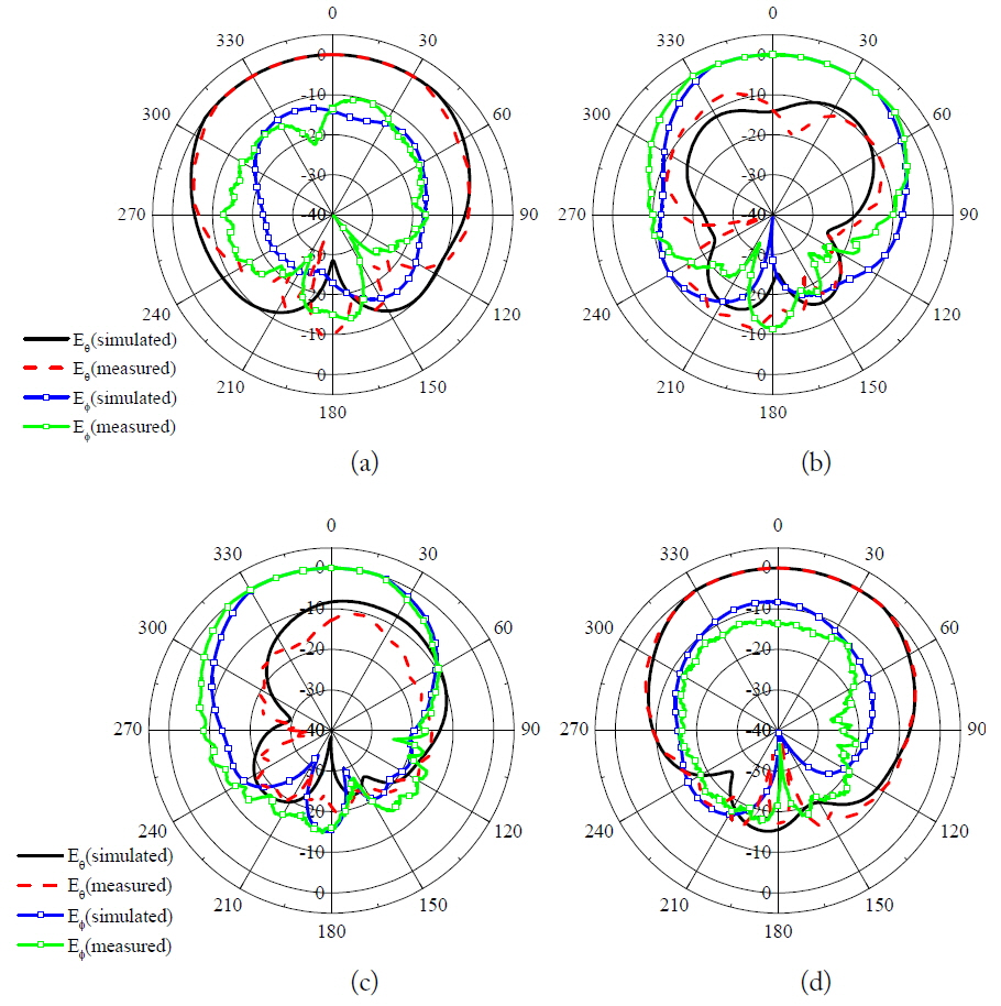
Simulated and measured radiation patterns of State II (diode # 1 is off and diode # 2 is on): (a) E-plane (yz plane) at 2.51 GHz, (b) H-plane (xz plane) at 2.51 GHz, (c) E-plane (yz plane) at 2.71 GHz, and (d) H-plane (xz plane) at 2.71 GHz.
IV. Conclusion
To produce dual-band polarization reconfigurability, the concept of loading a conventional square patch antenna with a via is experimentally investigated. First, the proposed structure works as a dual-band, dual-linear polarized antenna. The resonant frequencies of the proposed design are in the orthogonal polarization plane and have similar radiation characteristics. By properly selecting the size of the small patch with a shorting via, the second resonant frequency of the antenna can be adjusted. Owing to the simplicity of its structure, the proposed antenna is suitable for applications in wireless communications and mobile satellite communications.
Acknowledgments
This work was supported by the National Research Foundation of Korea funded by the Korean government (No. 2017R1A2B4010393).
References
Biography
Jeongin Kim is currently working toward his B.S degree in the Department of Electronic Engineering, Kyonggi University, Suwon, Korea. His research interests include antennas and electromagnetic wave propagation.

Youngje Sung was born in Incheon, Korea, in 1975. He received his B.S., M.S., and Ph.D. degrees from Korea University, Seoul, Korea, in 2001, 2002, and 2005, respectively. From 2005 to 2008, he was a senior engineer at the Antenna R&D Laboratory, Mobile Phone Division, Samsung Electronics, Korea. In 2008, he joined the Department of Electronic Engineering, Kyonggi University, Suwon, Korea, where he is currently a professor. His research interests include reconfigurable antennas, cellphone antennas, wideband slot antennas, multifunction devices, compact circular polarized antennas, and compact dual-mode filters. Prof. Sung serves as a reviewer for IEEE Transactions on Microwave Theory and Techniques, IEEE Transactions on Antennas and Propagation, IEEE Microwave and Wireless Components Letters, IEEE Antennas and Wireless Propagation Letters, Progress in Electromagnetic Research, IET Electronics Letters, and IET Microwaves, Antennas, and Propagation.

