Design of Small CRPA Arrays with Circular Microstrip Loops for Electromagnetically Coupled Feed
Article information
Abstract
This paper proposes a design of small controlled reception pattern antenna (CRPA) arrays using circular microstrip loops with frequencyinsensitive characteristics. The proposed array consists of seven identical upper and lower circular loops that are electromagnetically coupled, which results in a frequency-insensitive behavior. To demonstrate the feasibility of the proposed feeding mechanism, the proposed array is fabricated, and its antenna characteristics are measured in a full-anechoic chamber. The operating principle of the proposed feeding mechanism is then interpreted using an equivalent circuit model, and the effectiveness of the circular loop shape is demonstrated by calculating near electromagnetic fields in proximity to the radiator. The results confirm that the proposed feeding mechanism is suitable to have frequency-insensitive behavior and induces strong electric and magnetic field strengths for higher radiation gain in extremely small antenna arrays.
I. Introduction
Recent technical issues on controlled reception pattern antenna (CRPA) arrays are mainly focused on the employment of more antenna elements in an electrically restricted area [1–4]. However, the increasing number of antenna elements causes mutual coupling that degrades the impedance matching characteristics and radiation efficiency due to undesired shifts in the resonance frequencies [5, 6]. In addition, a typical rectangular patch antenna has frequency-sensitive characteristics due to its narrow matching bandwidth with an extremely steep reactance slope. Thus, a lot of efforts have been made to broaden the matching bandwidth by using additional parasitic elements, via pins, and external matching circuits [7–9]; however, these approaches increase the design complexity and require an additional layer to implement the extra structure. Although Kang et al. [10] proposed the design of rectangular microstrip loop antennas for a frequency-insensitive behavior with lower complexity, there has not been an in-depth consideration for reducing mutual coupling effects to further improve the antenna characteristics in extremely restricted areas.
In this paper, we propose the design of small CRPA arrays using circular microstrip loops with an electromagnetically coupled feed. The proposed array is composed of seven individual elements printed on high-dielectric ceramic substrates, and each element has upper and lower circular loops that are designed to resonate at 1.575 GHz and 1.227 GHz, respectively. The lower loop is fed by two output ports of an external hybrid chip coupler (XC1400P-03S; Anaren Inc., Syracuse, NY, USA) embedded on a printed circuit board (PCB) at the bottom of the array ground. The lower loop is fed by two output ports of an external hybrid chip coupler embedded on a PCB at the bottom of the array ground. The upper loop is then electromagnetically coupled by the near-fields radiated from the lower loop, and this feeding mechanism allows for frequency-insensitive behavior with lower reactance slope. Another advantage of this feeding structure is that the ratio between the electric and magnetic coupling strengths can be independently adjusted by varying the substrate thickness and the loop widths. Note that the tuning capability is essential for maximizing the antenna characteristics in small arrays by compensating for extra capacitance and inductance, which come from the strong mutual coupling. To verify the feasibility of the proposed feeding mechanism with circular microstrip loops, the seven-element array is fabricated, and its antenna characteristics are measured in a full-anechoic chamber. The operating principle of the proposed feeding mechanism is interpreted by building an equivalent circuit model, and the near electromagnetic fields are also observed to analyze the effectiveness of the circular loop shape. The results demonstrate that the proposed feeding mechanism is suitable to maintain a lower reactance slope and higher radiation gain in extremely small antenna arrays.
II. Proposed Circular Loop Antenna Array
Fig. 1 shows the geometry of the proposed seven-element CRPA array. The array has a circular ground with a radius of r, and its array elements are placed at a distance of m from the center of the ground. Each element is composed of upper and lower circular loops that are printed on high-dielectric ceramic substrates (ɛr = 20, tanδ= 0.0035) with thicknesses of h1 and h2. The upper and lower circular loops of each element are designed with diameters of l1 and l2 and widths of w1 and w2. The lower loop is directly fed by two output ports of an external hybrid chip coupler embedded on the PCB, and the upper loop is electromagnetically coupled to the lower loop. The circumferences of the upper and lower loops are then tuned for their resonate frequencies of 1.575 GHz and 1.227 GHz, respectively. Note that h1, w1, and w2 are important design parameters of the proposed feeding mechanism to adjust the ratio between the electric and magnetic coupling strengths for improved matching and radiation properties. The detailed design parameters are optimized by a genetic algorithm in conjunction with the FEKO EM simulator (Altair, Detroit, MI, USA) [11], and the optimized values are listed in Table 1.
Geometry of the proposed array: (a) perspective view and (b) side view of the Ant.1.

Optimized values of the proposed array
Fig. 2(a) presents a photograph of the proposed array printed on the ceramic substrate. Fig. 2(b) shows the PCB that includes the hybrid chip coupler with coplanar wave guides and 50-Ω termination chips for quadrature phase excitation. The antenna characteristics such as the reflection coefficient and active element pattern are measured in a full anechoic chamber, and the results will be discussed in Section III.

Photographs of the fabricated array: (a) top view and (b) bottom view.
III. Measurement and Analysis
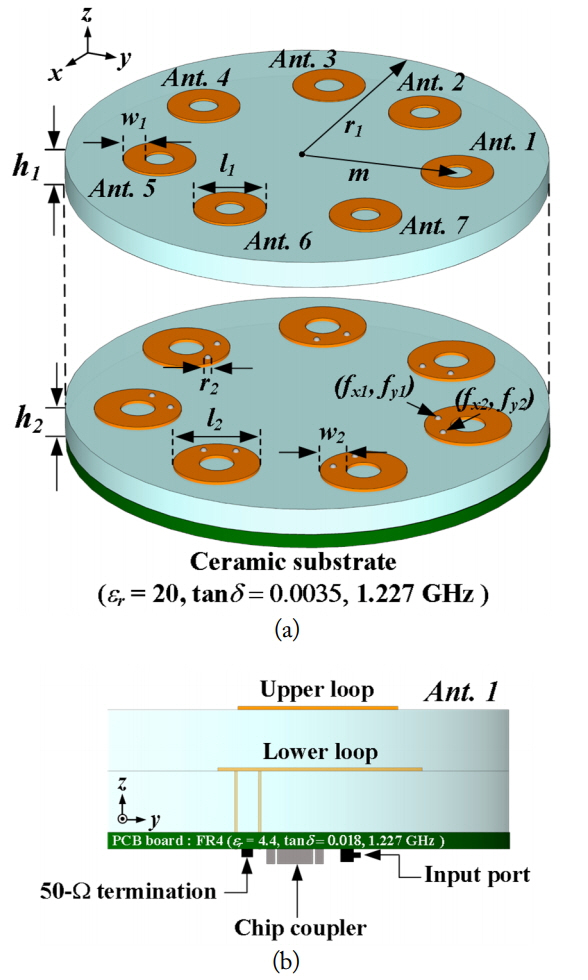
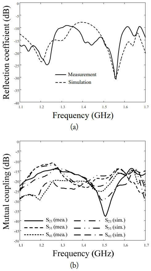
Fig. 3(a) shows the simulated reflection coefficients, specified by a dashed line, in comparison with measured results of the Ant.1. The results are obtained when Ant.1 is fed by a coaxial probe, while the other antennas are terminated by 50-Ω loads. The measured values are −17.71 dB and −24.76 dB at 1.575 GHz and 1.227 GHz, respectively. The simulated values are −17.71 dB and −24.76 dB at 1.575 GHz and 1.227 GHz, respectively. As can be seen, the simulated and measured reflection coefficients show similar tendency and maintain values less than −10 dB over a wide frequency range from 1.1 GHz to 1.7 GHz. This broadband impedance matching performance caused not only by the antenna characteristic, but also by the hybrid chip coupler where the reflected power at the antenna input port comes to the isolated port of the coupler in the operating frequency. Fig. 3(b) presents the mutual coupling between Ant.1, Ant.2, Ant.3, and Ant.4. Other cases are omitted because they have the same separation distances. The simulated and measured coupling strengths have similar tendency and less than −18 dB and −10 dB at 1.575 GHz and 1.227 GHz. Fig. 4 represents a comparison between the simulated and measured bore-sight gains of the Ant.1. The measured and simulated values are −3.2 dBic and −1.9 dBic at 1.575 GHz and −5.1 dBic and −4.6 dBic at 1.227 GHz.
S-parameters of the proposed array: (a) reflection coefficient and (b) mutual coupling.
Bore-sight gain of the proposed array (Ant.1).
The simulated antenna efficiencies for single antenna element without adjacent elements are 76% (1.575 GHz) and 83% (1.227 GHz), while the antenna efficiencies with adjacent array elements are 33% (1.575 GHz) and 28% (1.227 GHz). The gain deviation from 1.15 GHz to 1.65 GHz is less than 10 dB, which is lower than a typical patch antenna which uses only electric or magnetic coupled feeding mechanism. These results demonstrate that the proposed electromagnetically coupled feed structure can derive the frequency-insensitive behavior.
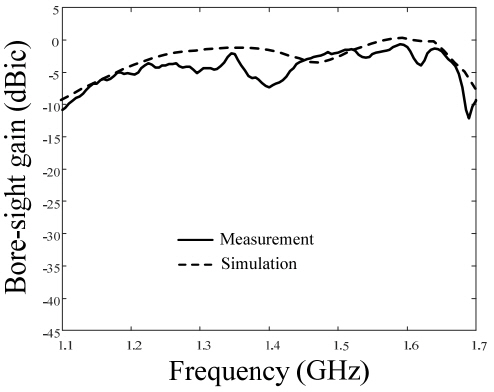
Fig. 5 provides an axial ratio of Ant.1 in the bore-sight direction. The antenna has simulated AR values of 2.8 dB and 5.1 dB at 1.575 GHz and 1.227 GHz, respectively, and the measured values are 3.8 dB at 1.575 GHz and 3.6 dB at 1.227 GHz. The AR values within the half-power beamwidth (HPBW) are listed in Table 2. The radiation patterns of Ant.1 in the zx- and zy-planes at GPS L1/L2 bands are shown in Fig. 6. The measured HPBWs at 1.575 GHz are 130° in the zx-plane and 115° in the zy-plane. The HPBWs at 1.227 GHz have values of 90° and 120° in the zx- and zy-planes, respectively. As expected, the antenna does not exhibit any serious pattern distortion in the upper hemisphere with HPBWs of greater than 90°, which is suitable for use in the CRPA applications.
Axial ratio of the proposed array (Ant.1).
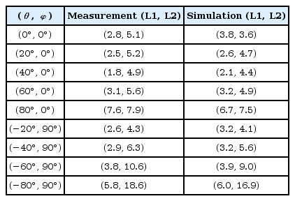
Axial ratio values of the proposed array (Ant.1)
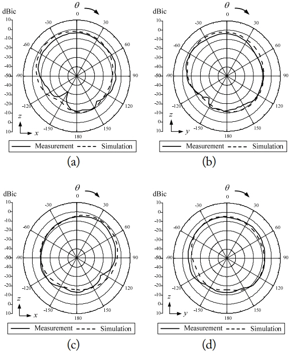
Radiation patterns of the proposed array (Ant.1): (a) zx-plane at 1.575 GHz, (b) zy-plane at 1.575 GHz, (c) zx-plane at 1.227 GHz, and (d) zy-plane at 1.227 GHz.
To interpret the operating principle of the proposed antenna from a circuit point of view, an equivalent circuit model is built using a data-fitting method, as shown in Fig. 7(a). The circuit describes the input impedance at port 1, while terminating the port 2 with 50-Ω impedance. The via pin connected to the lower loop is represented as inductance LF, and another parallel circuit, composed of RP, LP, and CP, is inserted to describe the higher-order resonance characteristic above 2 GHz. The lower loop is composed of RL2, LL2, and CL2, and the upper loop is specified by RL1, LL1, and CL1. These lower and upper loops are linked through the series capacitance Cc and the coupling coefficient k, which are associated with the electric and magnetic couplings, respectively. Note that the frequency-insensitive reactance variations can be obtained by employing the optimal ratio of Cc and k. The detailed values of the lumped elements are listed in Table 3, and the input impedance of the circuit is compared with that of the antenna obtained from the FEKO EM simulator, as illustrated in Fig. 7(b).
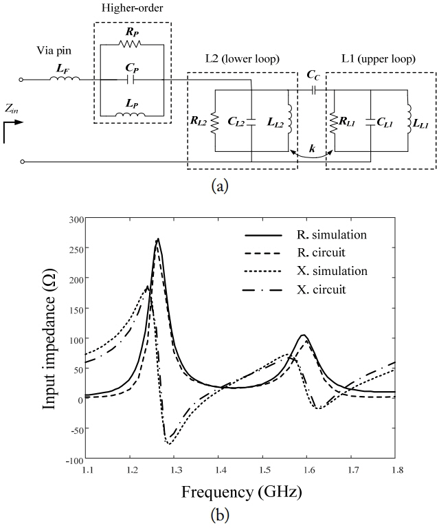
Equivalent circuit model and its input impedance: (a) circuit model and (b) input impedance.

Values of the lumped elements
To verify the advantage of the proposed feeding mechanism, we compare reactance variations with other feeding mechanisms using only electric or magnetic couplings, as shown in Fig 8. The dashed line represents the feeding mechanism that uses only the electric coupling after removing the inductive coupling coefficient k. The dotted line indicates the response when the capacitance Cc is removed. The results demonstrate that the proposed electromagnetic coupling with the solid line has a frequencyinsensitive reactance variation with lower reactance slope compared to other feeding mechanisms.

Reactance variations according to the feeding mechanism.
Fig. 9 shows the average electric and magnetic field distributions at 1.575 GHz and 1.227 GHz according to the shape of the loops. For a fair comparison, we optimized the circular and rectangular loops to resonate at same frequencies (1.575 GHz, 1.227 GHz) under the identical substrate diameter (r1 = 30 mm) and thickness (h1 = h2 = 6 mm). Fig. 9(a) presents a comparison of electric field distributions induced below the outer edge of the upper loop as specified by the dotted lines in the inset figure. The average field strengths are calculated according to the observation heights, and the results confirm that the circular loop maintains consistently higher field intensity. For example, the maximum difference is found at 11 mm with a value of 2.5 dB, which helps to achieve stronger electric coupling in the feeding mechanism. We also observed the magnetic field distributions induced at the highlighted area of the inset figure in Fig. 9(b). As similarly observed in the electric field distributions, the circular shape of the radiator helps to induce a stronger magnetic flux compared to the rectangular loop shape, which is required to achieve frequencyinsensitive behavior in such extremely small arrays. The anti-jamming characteristic can be observed by applying nulling algorithms such as the power inversion (PI) and least mean square (LMS), to the proposed antenna [12, 13].
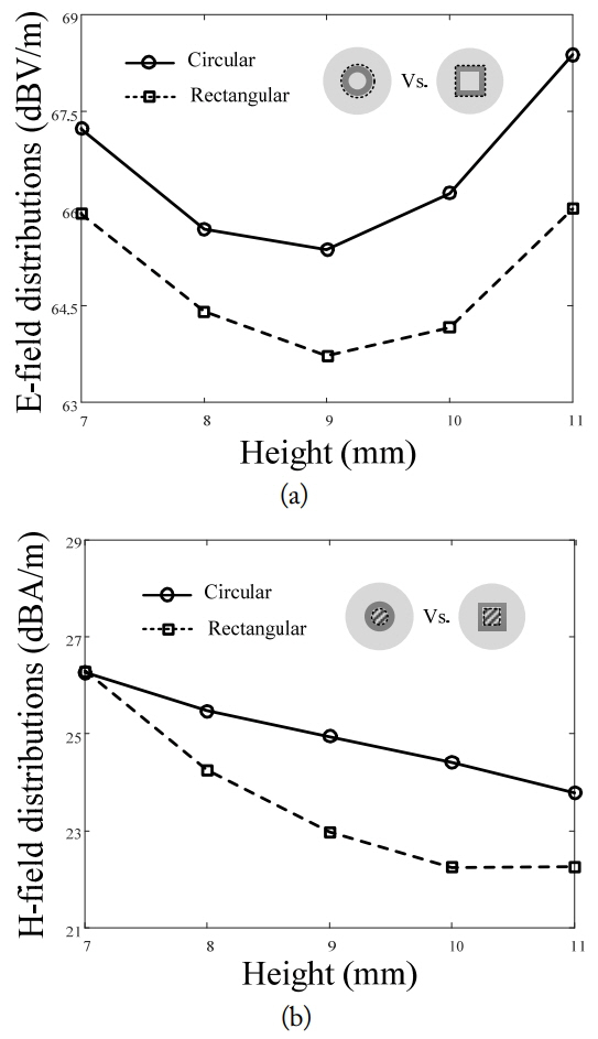
Average field distributions according to the shape of the loop: (a) E-field at edge of the loop, (b) H-field inside of the loop.
IV. Conclusion
We investigated the design of small CRPA arrays using the electromagnetically coupled feed with circular microstrip loops. The lower loop was fed by the external hybrid chip coupler, and the upper loop was electromagnetically coupled to the lower loop, which allowed for the frequency-insensitive behavior with the broadband circular polarization. The fabricated array showed measured reflection coefficients of −17.71 dB and −24.76 dB with bore-sight gains of −3.2 dBic and −5.1 dBic at 1.575 GHz and 1.227 GHz, respectively. In addition, the gain deviation between 1.15 GHz to 1.65 GHz was less than 10 dB. We also observed the near electromagnetic fields in proximity to the antenna and verified that the circular loop shape was capable of inducing stronger fields with the maximum improvement of 5.1 dB (electric field) and 7.0 dB (magnetic field). The results demonstrate that the proposed feeding mechanism is suitable to achieve the frequency-insensitive behavior with the lower reactance slope in the presence of strong mutual coupling.
Acknowledgments
This work was supported by the National Research Foundation of Korea (NRF) grant funded by the Korea government (MSIP) (No. NRF-2017R1D1A1B04031890) and in part by the Basic Science Research Program through the NRF funded by the Ministry of Education (No. 2015R1A6A1A03031-833).
References
Biography
Jun Hur received the B.S. and M.S. degrees in electronic and electrical engineering from Hongik University, Seoul, Korea, in 2014 and 2016, respectively. He is currently working toward the Ph.D. degree in electronics and computer engineering at Hongik University, Seoul, Korea. His research interests include the global positioning system antennas, antenna arrays, and position optimization of array elements for adaptive beamforming.

Hosung Choo received the B.S. degree in radio science and engineering from Hanyang University in Seoul in 1998, and the M.S. and Ph.D. degrees in electrical and computer engineering from the University of Texas at Austin, in 2000 and 2003, respectively. In September 2003, he joined the School of Electronic and Electrical Engineering, Hongik University, Seoul, Korea, where he is currently a full professor. His principal areas of research are the use of the optimization algorithm in developing antennas and microwave absorbers. His studies include the design of small antennas for wireless communications, reader and tag antennas for RFID, and on-glass and conformal antennas for vehicles and aircraft.

Gangil Byun received his B.S. and M.S. degrees in electronic and electrical engineering from Hongik University, Seoul, Korea in 2010 and 2012, respectively, and his Ph.D. degree in electronics and computer engineering from Hanyang University, Seoul, Korea in 2015. He joined the faculty of Ulsan National Institute of Science and Technology (UNIST) in February 2018 and is currently Assistant Professor of Electrical and Computer Engineering (ECE). Dr. Byun’s principal areas of research are in the design and analysis of small antenna arrays for adaptive beamforming applications, such as direction of arrival estimation, interference mitigation, and radar. His recent research interests also include circularly-polarized antennas, vehicular and aeronautic antennas, global positioning system antennas, antenna and array configuration optimization.