 |
 |
- Search
| J. Electromagn. Eng. Sci > Volume 18(2); 2018 > Article |
|
Abstract
In this paper, a method of designing a Vivaldi type phased array antenna (PAA) which operates at S-band (2.8–3.3 GHz) is presented. The presented antenna uses broadside coupled split ring resonators (BC-SRRs) for high isolation, wide field of view, and good active S-parameter characteristics. As an example, we design a 1 × 8 array antenna with various BC-SRR structures using theory and EM simulations. The antenna is fabricated and measured to verify the design. With the BC-SRR implemented between the two radiating elements, the isolation is shown to be enhanced by 6 dB, up to 23 dB. The scan angle is shown to be within ±53° based on a −10 dB active reflection coefficient. The operation of the scan angle is possible within ±60° with a little larger reflection coefficient (−7 dB to −8 dB). The proposed design with BC-SRRs is expected to be useful for PAA applications.
Over the past decades, the demand for phased array antennas (PAAs) has been growing rapidly with active research on them [1, 2]. The PAA is widely used for high gain beam-forming and -scanning in telecommunication [3], microwave imaging [4, 5], and radar applications [6]. Typical radiating elements of the PAA are the dipole, microstrip patch, and Vivaldi antenna. Among these, the Vivaldi antenna, also known as the flared notch or tapered slot antenna, is a traveling-wave type antenna of which the bandwidth is usually wider compared with the dipole and microstrip patch antennas, which are usually classified as resonant antennas supporting standing waves. There are three main types of Vivaldi antennas: the coplanar Vivaldi antenna (CVA), the antipodal Vivaldi antenna (AVA), and the balanced antipodal Vivaldi antenna (BAVA) [7]. When comparing these antennas’ characteristics, the CVA has a higher gain and directivity than the others. In addition, it offers the best side lobe level performance and relatively wide bandwidth [7]. When designing the PAA radiating elements, considerations should be given to issues such as the grating lobe, field of view (FOV), active S- parameters, and scan blindness [8]. The key factor involved in these issues is the mutual coupling among the radiating elements. This occurs dominantly between the adjacent radiating elements due to the surface wave flowing through the ground plane [9]. This not only degrades the isolation characteristics, but also causes deterioration of the various previously mentioned PAA characteristics.
A simple way to improve isolation may be to increase the physical distance between the radiating elements. However, if the distance is greater than half the free-space wavelength, a large grating lobe occurs in the backward direction when the main beam peak is scanned to near the forward endfire direction. Therefore, to enhance the isolation, while keeping the separation of the elements less than half the wavelength, various methods have been studied. Defected ground structure (DGS) [10, 11] and electromagnetic band gap (EBG) structures [12, 13] are some examples of them. The other metasurfaces [14], the RF fence [15], and some parasitic elements [8, 16] have also been studied and employed. In these methods, the mentioned structures are placed between the adjacent radiating elements to enhance the isolation. Although the enhancement of the isolation between the two neighboring radiation elements is important for PAA designs, it has been found that it does not always guarantee the required performances concerning the grating lobe, FOV, active S-parameters, and scan blindness.
In this paper, we present the method of designing a Vivaldi type PAA at 3 GHz with high isolation, wide FOV, good active S-parameter (or impedance) characteristics by employing a broadside coupled split ring resonator (BC-SRR) [17]. The ring resonator with a chip capacitor on it, the SRR using the side gap capacitance, and the BC-SRR using the capacitance between two layered planar rings have the stopband LC characteristic [18]. Since the two-layer Vivaldi is used for this work, the BC-SRR is the best candidate and is placed between the neighboring radiation elements. We design, fabricate, and measure a 1 × 8 CVA to validate the effects of the use of the BC-SRR in terms of the high isolation, wide scan angle, and active impedance. The full wave simulation results are compared with the measured ones with useful discussions.
First, we design a two-layer Vivaldi antenna at S-band (2.8–3.3 GHz, 16%) as a basic radiating element of a 1 × 8 PAA. The substrate is the Taconic TLY of which relative permittivity is 2.2.
A two-layer tapered slot (or Vivaldi) antenna element is shown in Fig. 1(a), in which a strip feed line is placed in the middle between the two metal planes. The double layered substrate thickness t is 3 mm. Fig. 1(b) shows a front view and side view of the designed antenna. The two metal planes have an exponentially tapered slot. The exponentially tapered slot acts as an impedance transformation network for a match between free space (377 Ω) and the slotline (50 Ω) [19, 20]. The tapered slotline dominantly supports a traveling wave. The stripline to slotline transition is obtained by optimizing C1, C2, and θ in Fig. 1(b).
In Table 1, the optimized dimensions of the structure for the required 10 dB return loss bandwidth are summarized.
Fig. 2 is the EM-simulated reflection coefficient and total gain. As shown in Fig. 3, the bandwidth of −10 dB reflection coefficient is 2.58–3.7 GHz (37%) and the antenna gain is 4.5 dBi.
The isolation between two radiating elements spaced 0.5λ0 is roughly only 15 dB. In this work, we will demonstrate the promising effects of BC-SRRs in the PAA designs.
The BC-SRR consists of two open conducting rings which are etched at both sides of a dielectric substrate and with the gaps in opposite positions [17]. The BC-SRR using the capacitance between two layered conducting rings has the stopband LC characteristic. Fig. 3(a) and (b) show the structures of a designed circular and square BC-SRR, respectively. They are made of copper and designed at 3 GHz. In Table 2, the dimensions of the designed BC-SRR are summarized.
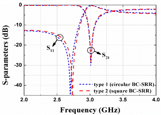
For more details determining the structure dimensions refer to [17, 18]. Fig. 4 shows the simulated S-parameters of type 1 and 2 BC-SRRs in the set-up shown in Fig. 3(c). The S21 transmission coefficients for both are −30 dB at 3.0 GHz. These results demonstrate that the stopband characteristic is well implemented in the structures at the target frequency.
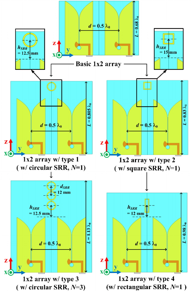
Based on the above results, we try to apply the BC-SRRs between the elements of a 1 × 2 Vivaldi type array antenna to enhance isolation. The type 1 and 2 resonators are placed with different numbers and shapes as shown in Fig. 5. The spacing d between the two radiating elements is 0.5λ0. The heights of type 1 and 2 are optimized for minimum mutual coupling. The optimized heights hSRR of types 1 and 2 are 12.5 mm and 15 mm, respectively. In an effort to further enhance the isolation, we have increased the number of BC-SRRs (type 3) or changed the shape (type 4) as shown in Fig. 5. Type 3 has three (N = 3) circular BC-SRRs. The spacing (dSRR) between the resonators is 12 mm. In type 4, a rectangular BC-SRR is used instead of a square (type 2). The optimized heights hSRR of types 3 and 4 are 12.5 mm and 12 mm, respectively.
Fig. 6 shows the S-parameters and radiation patterns of the 1 × 2 array antenna structures shown in Fig. 5. The S-parameters are plotted as a function of frequency for different types of the resonators. The radiation patterns show very little change. The details are summarized in Table 3. The isolation is enhanced by about 3 dB with type 4. This improvement will be shown to be more obvious with more array elements in Section III – 3.
We designed and analyzed the 1 × 8 array antennas extended from the 1 × 2 array antennas. Fig. 7(a)–(c) show the basic 1 × 8 array antenna, 1 × 8 array antenna with type 3 (circular BC-SRR, N = 3), and the same with type 4 (rectangular BC-SRR, N = 1), respectively. The spacing d between the radiating elements is 0.5λ0. The optimized dimensions of types 3 and 4, after many EM-simulations, are as follows: RSRR = 6 mm, dSRR = 13 mm (type 3), Lx = 5.5 mm, Lz = 17 mm (type 4), WSRR = 1 mm, GSRR= 1 mm, and hSRR = 21 mm (types 3 and 4).
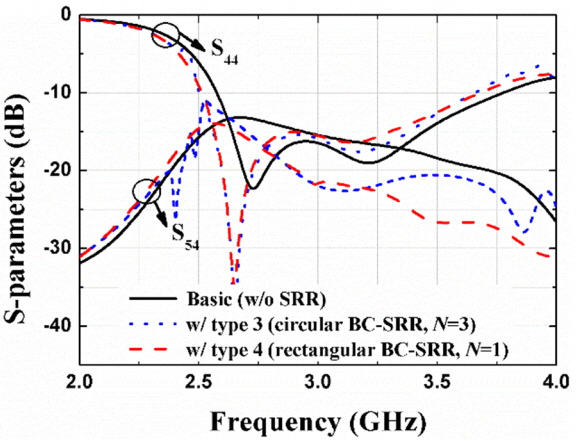
In Fig. 8, the EM-simulated S44 and S54 of the antennas in Fig. 7 are plotted. The bandwidth based on a −10 dB reflection coefficient (S44) is 2.5–3.6 GHz. We can see that it covers the target frequency band (2.8–3.3 GHz) with enough of a margin. The mutual couplings (S54) at 3 GHz when using type 3 and 4 resonators are shown to be about −23 dB, which is a 6 dB enhancement compared with the basic 1 × 8 array antenna.
Fig. 9 shows the EM-simulated active S44 (all ports from 1 to 8 excited) and total gains according to the scan angle θ0 for different antenna types.
For a beam peak at θ = θ0, the progressive excitation phase α is given by
where β0 is the propagation constant given by 2π/λ0 and the d is 0.5λ0.
The bandwidths based on a −10 dB active reflection coefficient (active S44) of the antennas with type 3 (with circular BC-SRR, N = 3) and type 4 (with rectangular BC-SRR, N = 1) are shown to cover the target frequency band (2.8–3.3 GHz) up to θ0 = 50°. The actual scan range of θ0 is from −53° to +53° based on the – 10 dB active reflection coefficient.
When θ0 = 60°, the active S44’s are shown not to satisfy −10 dB at the target frequency. It is about −8 dB at 3 GHz. The radiation patterns depending on the scan angles do not change. The realized scan angles of θ0 are shown to agree well with the targeted ones. While the total gains are similar for different antenna types, the active S44’s for the antennas with type 3 and 4 resonators are significantly lowered, especially for large scan angles. The radiation efficiencies decrease as θ0 increases. In Table 4, these results are summarized in detail.
According to Table 4, the overall performances of the type 3 and type 4 antennas may look similar. However, the structure of the type 4 antenna is simpler with only one rectangular BC-SRR.
In Fig. 10, the fabricated antenna and set-up for measurements are shown. Fig. 10(a) shows the fabricated basic single element, basic 1 × 8 array antenna and the proposed 1 × 8 array antenna (with rectangular SRR, N = 1, type 4). Fig. 10(b) and (c) show the set-ups to measure the reflection coefficients and radiation patterns, respectively.
Fig. 11 shows the EM-simulated reflection coefficients and total gains compared with measurements for the single element. The measured reflection coefficient has shifted to the left about 200 MHz from the simulated one, but the curve shapes are shown to reasonably agree. The EM-simulated gain at broadside is about 4.4 dBi, and the measured one is roughly 3.4 dBi.
Fig. 12(a) and (b) show the reflection coefficients S44 and mutual couplings S54 as a function of frequency. The measured S44 and S54 are shown to have also shifted to the left about 200 MHz from the simulated one. The measured S54’s of the basic and proposed 1 × 8 type 4 array antenna are 18 and 23 dB (enhanced by 5 dB), respectively. The measured total gains are 11.7 dBi, lower than the simulated by 1 dB.
The shifted frequencies were due to the hole made for the connection between the strip feedline and SMA connector, as seen in Fig. 10(a).
A 1 × 8 array antenna with BC-SRRs has been designed, fabricated, and measured. The total gains are maintained around 13 dBi, and the isolation is improved by about 6 dB with the BC-SRRs when compared with the basic 1 × 8 array antenna without them. The FOV is ±53° based on a −10 dB active reflection coefficient. The operation of the scan angle within 60° is possible with a little larger reflection coefficient of about −8 dB. The proposed design with BC-SRRs is expected to be useful for PAA applications.
Fig. 1
Designed double layered Vivaldi antenna element. (a) Structure of the designed single element. (b) Front and side view of the designed single element.
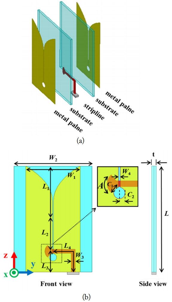
Fig. 2
Simulated reflection coefficient and total gain of single antenna element. (a) Reflection coefficient. (b) Total gain.
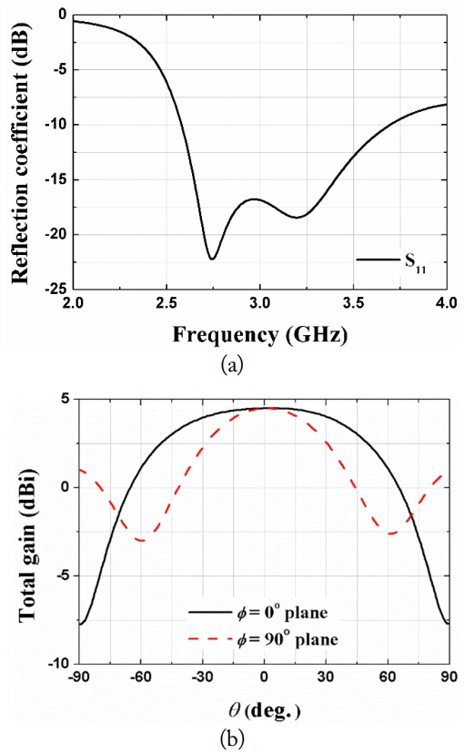
Fig. 3
Illustration of BC-SRRs and simulation set-up. (a) Unit of circular BC-SRR (type 1). (b) Unit of square BC-SRR (type 2). (c) Simulation set-up to extract the S-parameters.
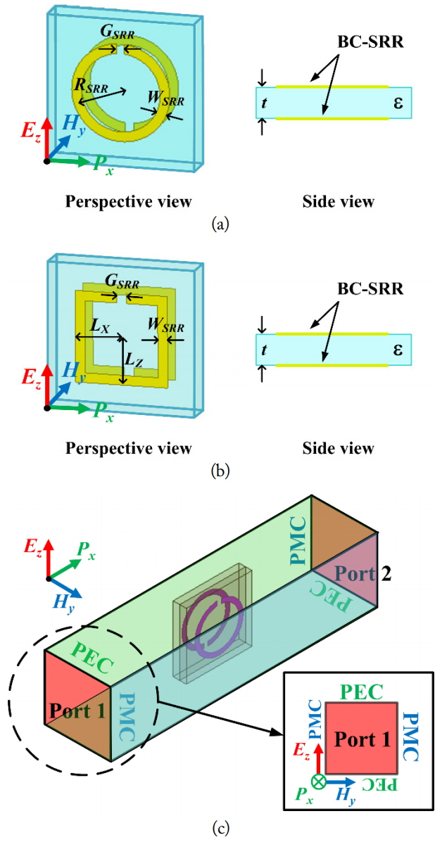
Fig. 6
Simulated S-parameters and total gain of the 1 × 2 array antennas. (a) S-parameters (S11, S21). (b) Total gain.
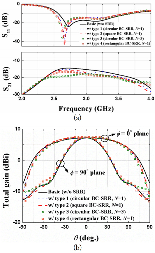
Fig. 7
Illustration of the 1 × 8 array antennas. (a) Basic (without SRR), (b) with type 3 (circular BC-SRR, N = 3) and (c) with type 4 (rectangular BC-SRR, N = 1).
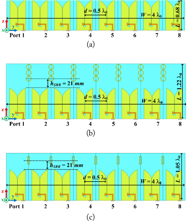
Fig. 9
Simulated active S-parameters and total gain comparison for different θ0’s. (a) Active S-parameters (S44) for different θ0’s. (b) Total gain for different θ0’s in the φ = 90° plane.
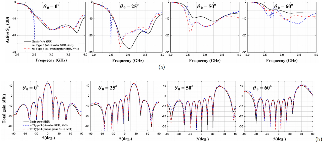
Fig. 10
Fabricated antenna and set-up for measurements. (a) Fabricated antenna. (b) Set-up to measure reflection coefficients. (c) Setup to measure radiation patterns.

Fig. 11
EM-simulated and measured (a) reflection coefficients and (b) total gains of a single element.
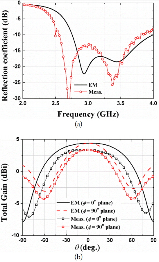
Fig. 12
EM-simulated and measured (a) reflection coefficients, (b) mutual couplings, and (c) total gains of 1 × 8 array antennas.

Table 1
Design parameters of Vivaldi antenna elements (unit: λ0 at 3 GHz, λ0 = 10 cm)
Table 2
Dimensions of designed BC-SRRs (unit: mm)
Table 3
Optimized antenna length L (Fig. 5) and gains of different 1 × 2 array antennas (at 3.0 GHz)
| 1 × 2 array antenna type | L (λ0) | Isolation (dB) | Gain (dBi) |
|---|---|---|---|
| Basic (w/o SRR) | 0.68 | 15.3 | 7.17 |
| w/ type 1 | 0.805 | 17.2 | 7.17 |
| w/ type 2 | 0.83 | 17.1 | 7.43 |
| w/ type 3 | 1.13 | 18.1 | 7.31 |
| w/ type 4 | 0.98 | 18.3 | 7.55 |
Table 4
Simulated active bandwidths, total gains, radiation efficiencies and isolations of the antennas for different θ0’s
REFERENCES
1. P Rocca, G Oliveri, RJ Mailloux, and A Massa, "Unconventional phased array architectures and design methodologies: a review," Proceedings of IEEE, vol. 104, no. 3, pp. 544–560, 2016.

2. E Brookner, "Advances and breakthroughs in radars and phased-arrays," In: Proceedings of 2016 IEEE International Symposium on Phased Array Systems and Technology; Waltham, MA. 2016;pp 1–8.

3. T Jagadesh and BS Rani, "Actualization of a phased array antenna utilizing digital beamforming," In: Proceedings of 2016 International Conference on Control, Instrumentation, Communication and Computational Technologies; Kumaracoil, India. 2016;pp 111–116.

4. M Moosazadeh, S Kharkovsky, JT Case, and B Samali, "Antipodal Vivaldi antenna with improved radiation characteristics for civil engineering applications," IET Microwaves, Antennas and Propagation, vol. 11, no. 6, pp. 796–803, 2017.

5. M Moosazadeh, S Kharkovsky, JT Case, and B Samali, "Improved radiation characteristics of small antipodal Vivaldi antenna for microwave and millimeter-wave imaging applications," IEEE Antennas and Wireless Propagation Letters, vol. 16, pp. 1961–1964, 2017.

6. M Han, J Kim, D Park, H Kim, and J Choi, "Dual polarized array antenna for S/X band active phased array radar application," Journal of the Korean Institute of Electromagnetics and Science, vol. 10, no. 4, pp. 309–315, 2010.


7. Nurhayati, E Setijadi, and G Hendrantoro, "Comparison study of S-band Vivaldi-based antennas," In: Proceedings of 2016 IEEE Region 10 Symposium (TENSYMP); Bali, Indonesia. 2016;pp 188–193.

8. Z Xu, C Zhang, T Kaufmann, X Yan, Y Yuan, and C Fumeaux, "Analysis of scan blindness in a linearly polarized tapered-slot phased array in triangular lattice performance improvement with parasitic notches," IEEE Transactions on Antennas and Propagation, vol. 62, no. 8, pp. 4057–4066, 2014.

9. A Kedar and KS Beenamole, "Wide beam tapered slot antenna for wide angle scanning phased array antenna," Progress in Electromagnetics Research B, vol. 27, pp. 235–251, 2011.

10. MI Ahmed, A Sebak, EA Abdallah, and H Elhennawy, "Mutual coupling reduction using defected ground structure (DGS) for array applications," In: Proceedings of the 15th International Symposium on Antenna Technology and Applied Electromagnetics; Toulouse, France. 2012;pp 1–5.

11. S Kaushik, SS Dhillon, and A Marwaha, "Rectangular microstrip patch antenna with U-shaped DGS structure for wireless applications," In: Proceedings of the 5th International Conferences and Computational Intelligence and Communication Networks; Mathura, India. 2013;pp 27–31.

12. Q Li, AP Feresidis, M Mavridou, and PS Hall, "Miniaturized double-layer EBG structures for broadband mutual coupling reduction between UWB monopoles," IEEE Transactions on Antennas and Propagation, vol. 63, no. 3, pp. 1168–1171, 2015.

13. N Ma and H Zhao, "Reduction of the mutual coupling between aperture coupled microstrip patch antennas using EBG structure," In: Proceedings of 2014 IEEE International Wireless Symposium; X’ian, China. 2014;pp 1–4.

14. CH Park and HW Son, "Mutual coupling reduction between closely spaced microstrip antennas by means of H-shaped conducting wall," Electronics Letters, vol. 52, no. 13, pp. 1093–1094, 2016.

15. FY Kuo and RB Hwang, "High-isolation X-band marine radar antenna design," IEEE Transactions on Antennas and Propagation, vol. 62, no. 5, pp. 2331–2337, 2014.

16. J Ghosh, S Ghosal, D Mitra, and SR Bhadra Chaudhuri, "Mutual coupling reduction between closely placed microstrip patch antenna using meander line resonator," Progress in Electromagnetics Research Letters, vol. 59, pp. 115–122, 2016.

17. MJ Freire, MA Lopez, F Meise, JM Algarin, PM Jakob, M Bock, and R Marques, "A broadside-split-ring resonator-based coil for MRI at 7 T," IEEE Transactions on Medical Imaging, vol. 32, no. 6, pp. 1081–1084, 2013.


18. D Jeon and B Lee, "Simplified modeling of ring resonators and split ring resonators using magnetization," Journal of Electromagnetic Engineering and Science, vol. 13, no. 2, pp. 134–136, 2013.


Biography
Sungyoun Hwang received his B.S. degree in information and communication engineering from Soonchunhyang University, Asan, Korea, in 2015. He is currently working toward a master’s degree in electronics and radio engineering from Kyung Hee University. His fields of research include wireless power transfer systems, passive devices, and small antennas.

Biography
Dong Hwan Kim received his B.S. degree in electronics engineering from Inje University, Gimhae, Korea, in 2005, and his M.S. degree in electronics engineering from Kyungpook National University, Daegu, Korea, in 2007. He is currently working at Hanwha Systems. His research interests include active phased array antenna design and multi-function radar system.

Biography
Bomson Lee received his B.S. degree in electrical engineering from Seoul National University, Seoul, Korea, in 1982. From 1982 to 1988, he was with the Hyundai Engineering Company Ltd., Seoul, Korea. He received his M.S. and Ph.D. degrees in electrical engineering from the University of Nebraska, Lincoln, NE, USA, in 1991 and 1995, respectively. In 1995, he joined the faculty at Kyung Hee University, where he is currently a professor in the Department of Electronics and Radio Engineering. From 2007 to 2008, he was the chair of the technical group for microwave and radio wave propagation at the Korea Institute of Electromagnetic Engineering and Science (KIEES). In 2010, he was an Editor-in-Chief of the Journal of the KIEES. Since 2015, he has been a vice-chairman of KIEES. His research activities include microwave antennas, RF identification (RFID) tags, microwave passive devices, wireless power transfer, and metamaterials.

Biography
Joon Young Park received his B.S. degree in electronics engineering from Dong-A University, Busan, Korea, in 1997 and his M.S. degree in electronics engineering from Kyungpook National University, Daegu, Korea, in 1999. He was a senior researcher at Gammanu, Suwon, Korea, where he was involved with the development of various antennas, including base station antennas for communication systems. Since 2002, he has been working at Hanwha Systems, Yongin, Korea, where he is a chief engineer. His research interests include phased array antenna systems, design of active array, and advanced optimization algorithms for array antenna and radar applications.

- TOOLS


