I. Introduction
The bandpass filtering impedance transformer (IT) is rapidly developing in modern communication systems. This IT is increasingly becoming necessary in many applications, such as power dividers [1], antenna feeding lines [2], and amplifier design [3]. Indeed, a conventional quarter-wavelength transformer is a well-known IT [4], but this network has some limitations, such as difficulty in the realization of a high impedance transforming ratio and poor out-of-band suppression. In recent years, various structures of filtering IT have been proposed [5ŌĆō11]. A mixed lumped and distributed IT with low-pass filtering response is designed in [5]. However, the shunt capacitors can produce a self-resonance frequency, which introduces additional parasitic effects at high frequency. Wideband ITs are proposed using an open-circuit parallel-coupled line with an interconnecting transmission line (TL) [6] and a multiple-section stepped-impedance TL with input/output couplings [7]. However, their impedance transforming ratio is low. In [8], an open-circuit stub coupled-line IT with a bandpass filtering response is designed to transform 20 ╬® to 50 ╬®. In [9], a bandpass response coupled-line IT with an ultra-high impedance transforming ratio is presented by using two-section open-ended coupled lines. This IT is applicable to low termination impedance. Therefore, a short-ended coupled-line IT with an ultra-high impedance transforming ratio is proposed [10] for high load termination impedance. High selectivity is obtained by increasing the number of stages, but the insertion loss is degraded. Moreover, the stopband characteristic is limited. In [11], a bandpass filtering IT is designed with a section of open-ended coupled lines and an open-circuit stub TL. The transformer is valid for low termination impedances at the source and/or load terminals.
In this study, an IT with a short-circuit stub parallel-coupled line and a TL with a bandpass filtering response is presented. The proposed network can be applied to high load termination impedance. A short-circuit stub TL can produce several transmission zeros in the stopband. Moreover, a bandpass filtering response with high selectivity can be obtained.
II. Design Equation
Fig. 1(a) shows the schematic of the proposed IT, which is composed of a short-end parallel-coupled line and a short-circuit stub TL with a characteristic admittance of Y1 connected at coupling port 2 of the coupled line. The electrical lengths of the parallel-coupled line (╬Ė) and the short-circuit stub TL (2╬Ė) are given as a quarter-wavelength (╬╗/4) and a half-wavelength (╬╗/2) at f0, respectively. A short-circuit stub TL is used to create two transmission poles in the passband and three transmission zeros in the stopband [11], where the transmission zeros are located on the lower and upper sides of the passband, respectively. The proposed circuit is efficient at high termination impedance. Fig. 1(b) shows the schematic of the impedance transformer in [11] with an open-end parallel-coupled line and an open-circuit stub TL. The network is used only for low termination impedance.
The reflection and transmission coefficients of the proposed IT network, where input port 1 and output port 3 are terminated with the admittances YS and YL, respectively, can be derived as (1).
where
Moreover, YS = 1/ZS, YL = 1/ZL, Y0e = 1/Z0e, and Y0o = 1/Z0o. By solving (1a), the even-mode characteristic admittance Y0e of the coupled line with the specified S11, YS, and r at f0 can be derived as (3).
where
r is an impedance transforming ratio of ZS to ZL. S11 and Y0o are the predefined magnitude of return loss and odd-mode admittance of the coupled line at f0, respectively. By giving (1a) equal to zero, the characteristic admittance of Y1 can be derived as (5).
From the above design equations, the relationship of Z0e and Z0o with r is plotted in Fig. 2. Z0e dramatically decreases as r increases. With the same r, Z0e increases as Z0o increases. Therefore, a higher r requires a relatively looser coupling than a lower r, where the coupling coefficient is given by C = 20 log[(Z0e ŌĆō Z0o)/(Z0e + Z0o)] [dB]. The calculation is conducted by choosing ZL = 50 ╬®, S11 = ŌłÆ20 dB at f0, Z0o = 27 ╬®, 30 ╬®, 35 ╬®, and r varies from 2 to 12.
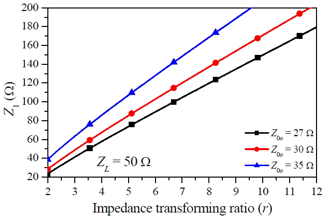
Similarly, Fig. 3 shows the variations of Z1 according to r and Z0o. Z1 increases as r increases. Moreover, Z1 increases more with a higher Z0o. As shown in Figs. 2 and 3, a low r prevents the realization of the coupled line, whereas a high r hinders the realization of a short-circuit stub TL. Therefore, a trade-off between r and the characteristic impedances of Z1 and Z0e is required.
Fig. 4 shows the S-parameter characteristics of the proposed IT with different r. The stopband attenuation is improved with a high r; but the bandwidth of the passband becomes narrow. Moreover, two transmission poles occur in the passband.
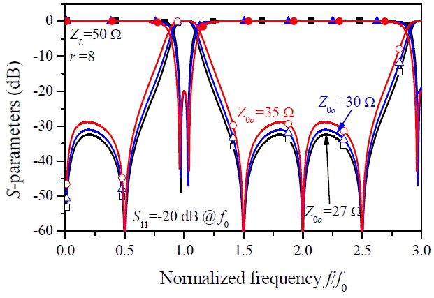
Transmission zeros are produced in the stopband, and a wide stopband characteristic can be obtained. Transmission zeros at 0.5f0, 1.5f0, and 2.5f0 are produced by a short-circuit stub TL. Moreover, a transmission zero at 2f0 is produced by a coupled line. The simulation is conducted by fixing Z0o = 27 ╬® and varying r = 4, 6, 8, and 10. Fig. 5 illustrates the S-parameter characteristics of the proposed IT with different Z0o. The bandwidth of a 20 dB return loss is improved with a high Z0o, but the stopband attenuation is degraded. The simulation is conducted by fixing r = 8 and varying Z0o = 27 ╬®, 30 ╬®, and 35 ╬®. The calculated values of all variables of the simulation in Figs. 4 and 5 are shown in Table 1.
III. Simulation and Measurement Results
An experimental validation was conducted by designing the IT and fabricating it on an RT 5880 substrate, with ╔ør = 2.2 and h = 0.787 mm. The proposed IT network with a 400ŌĆō50 ╬® (r = 8) of termination impedance, Z0o = 27 ╬®, and reflection coefficient of 20 dB at f0 = 2.6 GHz was designed. All the calculated variables are listed in Table 1. An electromagnetic (EM) simulation was performed using the Ansoft HFSS v15.
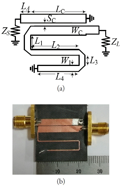
Fig. 6 shows the EM simulation layout and photograph of the fabricated IT network. The physical dimensions of the fabricated circuit are listed in Table 2. To minimize the circuit size, a half-wavelength short-circuit stub TL is designed as a mean-der structure. The overall circuit size of the proposed IT is 24 mm ├Ś 16 mm.
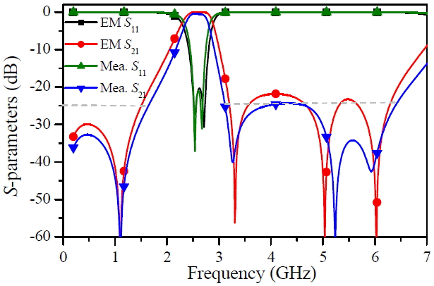
Fig. 7 illustrates the EM simulation and measurement results. The measured results are in good agreement with the simulations. The insertion and return losses are obtained 0.6 dB and 22.5 dB at f0, respectively. Similarly, the bandwidth of the 20 dB return loss is 0.19 GHz, which extends from 2.51 GHz to 2.7 GHz. The insertion loss of the passband is better than 0.8 dB. Moreover, one transmission zero on the lower side and three transmission zeros on the upper side of the passband are obtained, and these transmission zeros provide a wide stopband characteristic. The lower- and upper-side stopband attenuations of 25 dB are obtained from dc to 1.64 GHz and from 3.12 GHz to 6.4 GHz, respectively.
IV. Conclusion
An IT with a bandpass filtering response for high termination impedance is proposed and demonstrated in this study. The designed equations are derived with a predefined return loss. To show the validity of the proposed analysis, an IT is designed, fabricated, and measured. The simulated and measured results agree well with the analysis. The proposed IT with high selectivity, multi-transmission zeros, and bandpass response can be obtained simultaneously. The proposed IT is simple to design and is expected to be applied in various applications, such as baluns, power dividers, and antenna feeding lines.


