A Wideband Doherty Combiner with Phase Variation Compensation Using LTCC Applicable for High Power Transmission
Article information
Abstract
In this paper, we propose a small-sized Doherty combiner with phase variation compensation using low temperature co-fired ceramic (LTCC) substrate. The proposed design theory for the Doherty combiner is derived using the phase calculation of the S-parameter based on the relation between the input and output ports. The proposed circuit is designed after determining the band edge frequency and the targeted degree of the phase balance. The proposed circuit is verified using the microstrip line and the LTCC substrate. The implemented structure, using LTCC as the substrate, is operated under a high-power test of continuous wave 50 W, the results of which also show that the amplitude and phase balance have variations within 0.2 dB and ±1°, respectively. The high-power test shows that the implemented structure is applicable for high power Doherty amplifiers or combiners.
I. Introduction
A power amplifier (PA) is an important component that satisfies the requirements of high linearity and high-power efficiency in a radio frequency (RF) communication system. The PA generally operates near the saturation region to achieve maximum power efficiency. However, the power efficiency of a PA undergoes degradation due to distortions in output signals. Furthermore, its efficiency degrades if the PA operates at power levels below the saturation region. As efficiency decreases, most of the power diverges to produce heat, which deteriorates the characteristics of the amplifier and causes various issues, including heat generation and heat dissipation problems [1–2]. The Doherty power amplifier (DPA) possesses the advantages of easy implementation and high-power efficiency, although it is widely known to suffer from the disadvantage of a narrow bandwidth.
Therefore, many studies [3–9] have attempted to improve the narrow bandwidth of the DPA. For this purpose, previous studies have used a two-stepped transmission line impedance transformer [3], a branch line structure with a splitter and a combiner [4–5], and the addition of resonance circuits [6–8] or an additional line [9]. However, these previous designs occupy large combiner areas on their substrates due to the λ/4 or λ/2 electrical lengths of their microstrip lines.
In this paper, a Doherty combiner is implemented to improve the phase bandwidth and reduce the size of the proposed combiner using low temperature co-fired ceramic (LTCC) as the substrate. In addition, the desired target specification is satisfied as a result of the continuous wave (CW) 50 W high power test, suggesting the possibility of not only miniaturization but also high-power RF systems.
II. Design Theory
The basic structure of the Doherty power amplifier is composed of a carrier amplifier, a peaking amplifier, and a combiner region, as depicted in Fig. 1(a). The carrier amplifier stage is combined at
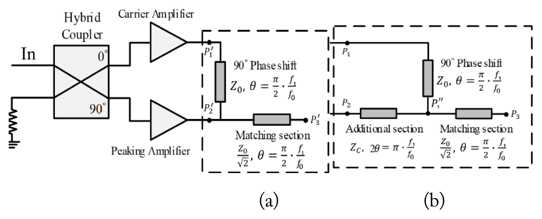
Block diagram of the Doherty power amplifier with (a) a conventional combiner, and (b) the proposed output combiner.
where,
Assuming that the phase differences of ∡S31 and ∡S32 at center frequency f0 is ∅︀, the phase difference ∅︀0 between the two inputs of the proposed structure at f0 is
The proposed circuit has a center frequency of 3.5 GHz, while the phase deviation is set to 2° at an edge frequency of 3.6 GHz. Finally, the ZC of the additional transmission line is obtained by solving
III. 3D Structure and Fabrication Results
The proposed circuit is implemented using an LTCC substrate with a dielectric constant of 6 for a small-sized Doherty combiner, as shown in Fig. 2. The ground L2 is added in order to integrate three transmission lines into one chip. The thickness of the chip from L1 to L3, as depicted in Fig. 2(a) and 2(b), is controlled through the characteristic impedance equations of the strip line. One of the three lines is for the 180° electrical length of the additional section, while the other two lines are for the 90° phase and the matching section.
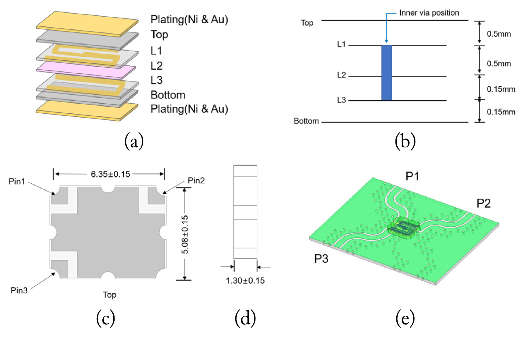
(a) LTCC diagrams with several layers, (b) side diagrams of the LTCC, (c) top dimension, (d) side dimension, and (e) 3D structure with PCB substrate.
Since the characteristic impedance ZC of the additional section has 38.81 Ω with a 180° electrical length, the additional line is located at the L3 layer, which is 0.15 mm away from the bottom ground (GND).
To apply a 180° line within a 6.35 mm × 5.08 mm size, as shown in Fig. 2(c)–2(e), the height of the layer from the GND is reduced to realize a wider line width for ZC. The two lines for the 90° phase shift and the matching section are implemented in one layer. The L1 and L3 layers are connected at the

Comparison results of the conventional, proposed 3D structure, and measured results: (a) magnitude, (b) output phase difference, (c) insertion loss, (d) return loss, and (e) phase balance.
IV. High Power Test of DUT
Fig. 4(a) shows the PCB jig with the LTCC substrate implemented as the Device Under Test (DUT). The high-power test (HPT) is used for checking RF performances when high power is conducted by the test jigs. Fig. 4(b) depicts the setup for the HPT. The equipment required for the HPT process consists of a signal generator, a power amplifier, a power meter, an isolator, a coupler, a termination component, and two test jigs. The signal generator produces a signal, which the power amplifier amplifies, while the power meter checks whether 50 W power is appropriately supplied. The HPT procedures are as follows:

(a) PCB jig with DUT, (b) setup diagram for the high-power test.
1. The experimental setup for the high-power test is organized, as shown in Fig. 4(b).
2. Two DUTs are linked with each other in a back-to-back connection—the P3 of the first DUT signifies the input port, while the P3 of the second DUT signifies the output port.
3. A 50-W CW at 3.6 GHz is applied to the P3 of the first DUT for 5 minutes.
4. The other DUTs are also tested in the same manner.
The HPT results highlight that the amplitude and phase balance have variations within 0.2 dB and ±1°, respectively, as shown in Fig. 5. Therefore, the proposed Doherty combiner using LTCC operates well, with fewer variations in phase balance, even under 50 W CW conditions.
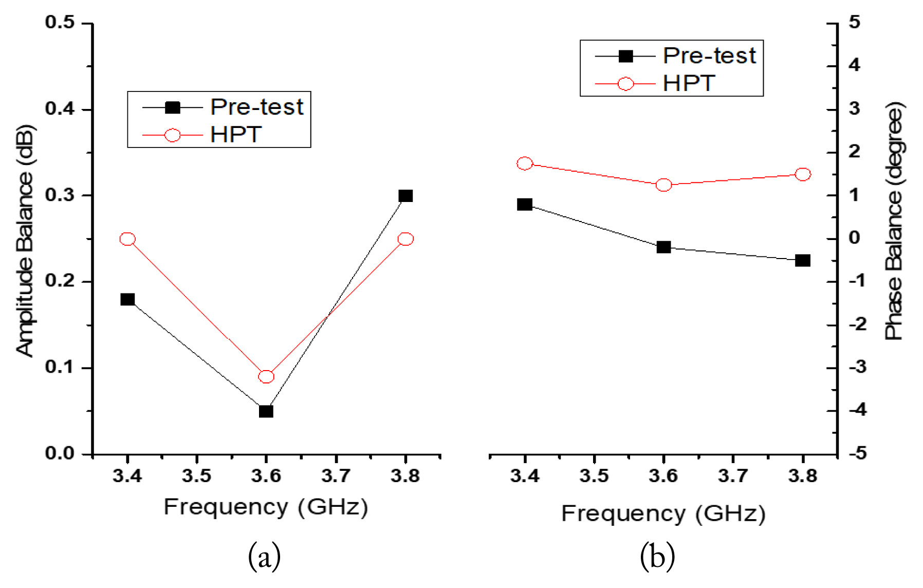
Pre- and post-high-power test: (a) amplitude balance and (b) phase balance.
V. Conclusion
In this paper, a small-sized Doherty combiner using LTCC substrate is proposed. The structure sets the selected frequency of f1 and the targeted degree of phase balance. Thus, the characteristic impedance with a 180° line can be obtained in the additional section of the combiner from the proposed design theory. Furthermore, to minimize the circuit size, the proposed circuit was implemented using three layers in the LTCC substrate. For the wideband application of the Doherty power amplifier, the proposed circuit was operated under CW 50 W at 3.6 GHz. The amplitude and phase balance were found to be less than 0.06 dB and ±1°, respectively. Therefore, the proposed circuit is applicable for use in miniaturized high power Doherty Power amplifiers and small-sized high-power combiners in future communication systems.
Acknowledgments
These results are supported by the Regional Innovation Strategy (RIS) through the National Research Foundation of Korea (NRF), funded by the Ministry of Education (MOE) (No. 2021RIS-004) and the Soonchunhyang University Research Fund.
References
Biography

Youna Jang received her master’s degree in Display Engineering from Hanyang University, Seoul, Korea, in 2014. She also received her Ph.D. in Electrical Communication System Engineering from Soonchunhyang University, Choongnam, Korea, in 2019. She participated as a designer of the Duplexer filter in an internship program in 2015 at Qorvo, Bundang, South Korea. She was a lecturer at Soonchunhyang University from 2016 to 2020. She is currently a research professor at the Radio and Mechatronics Research Center. Her research areas include the design of passive components in microwave bands.

Kwanhun Jeong was born in Mokpo, Korea, in 1994. He received his B.E. degree in Electrical Engineering from Soonchunhyang University, Asan, Korea, in 2020. Currently, he is an M.E. student at Soonchunhyang University. His current research interests include RF passive device theory, design, and testing.

Jiwon Kim was born in Seoul, Korea, in 1994. She received her M.E. degree in Electrical Communication System Engineering from Soonchunhyang University, Asan, Korea, in 2019. Currently, she is a Ph.D. student at Soonchunhyang University. Her current research interests include RF passive device and filter design, and process design kit (PDK).
Daeung Lee was born in Korea in 1989. He received his Ph.D. degree in Electrical and Communication System Engineering from Soonchunhyang University, Asan, Korea, in 2019. Currently, he works for Huba. His current research interests include RF passive elements theory, design, and multi-layer passive device design.
Dal Ahn received his B.S., M.S., and Ph.D. degrees in Electronics from Sogang University, Seoul, Korea, in 1984, 1986, and 1990, respectively. From 1990 to 1992, he worked with the Mobile Communications Division, Electronics, and Telecommunications Research Institute (ETRI), Daejeon, Korea. Since 1992, he has been affiliated with the School of Electrical and Electronic Engineering, Soonchunhyang University, Asan, Chungnam, Korea, where he is currently a professor. Currently, he is also the chief of the RF and Microwave Component Research Center (RAMREC), Soonchunhyang University. He is also a technical consultant for Tel Wave Inc., Suwon, Korea. His current research interests include the design and application of passive and active components at radio and microwave frequencies, the design of RF front-end modules for various handset systems using low-temperature co-fired ceramic (LTCC) technology, DGS circuit applications, and circuit modeling using a commercial EM analysis program. Prof. Ahn is also an editor of the Journal of Korea Electromagnetic Engineering Society and a senior member of the Korea Electromagnetic Engineering Society (KEES).