High-Q Transformer Neutralization Technique for W-Band Dual-Band LNA Using 0.1 μm GaAs pHEMT Technology
Article information

Abstract
In this study, a dual-band low-noise amplifier (LNA) was implemented by applying a transformer-based neutralization technology to the W-band. Incorporating the neutralization technique was difficult owing to performance degradation in the W-band. However, circuit performance was enhanced thanks to the layout optimization of transformer-based neutralization networks, and the improved operation was confirmed in the W-band. The neutralization technique was implemented in four stages with a 0.1-μm gallium arsenide (GaAs) pseudomorphic high-electron-mobility-transistor monolithic microwave integrated circuit LNA. The LNA showed small signal gains of 20.3 dB and 21.7 dB and noise figures of 5.0 dB and 6.4 dB (at 84 GHz and 96 GHz, respectively) while consuming 46 mW from a 1-V supply.
I. Introduction
Multi-band circuits employing millimeter waves (mmW) and up to the W-band (75–110 GHz) are attracting considerable interest owing to their potential in high-performance applications related to autonomous driving radars, high-speed mobile communications, imaging systems, and ultrafast wireless communications [1]. W-band communication and radar applications are mainly concentrated in two frequency bands (Band_L, 81–86 GHz; Band_H, 94–97 GHz). Accordingly, W-band low-noise amplifiers (LNAs) must be designed with broadband or multiband topology [1, 2].
However, in the case of mmW, as the frequency increases, the parasitic capacitance of transistors significantly deteriorate circuit performance. These degrade the operating frequency, maximum gain, and bandwidth, affecting system sensitivity and dynamic range. Therefore, mmW circuits generally use a neutralization technique that enhances performance by neutralizing the parasitic capacitance of transistors.
A neutralization technique mitigates the transistors’ parasitic capacitances, i.e., the gate-drain (Cgd) and drain-source (Cds) capacitances. Among the various neutralization techniques [3–6], the transformer-based feedback structure is more suitable for multiband circuits and mmW amplifiers [3]. This is implemented by reusing the input and output bias lines of the transistors. Thus, the performance is enhanced without any increase in the chip area or power consumption.
Unfortunately, neutralization techniques are not easily applied in the W-band. To apply neutralization technology in the W-band, it is essential to implement sufficiently small and high-quality capacitors. However, high-Q neutralization techniques are challenging to implement due to parasitic inductances generated by the capacitor itself and the circuit layout. Therefore, various previous studies have been reported to minimize unnecessary parasitic components using layout optimization and 3D electromagnetic simulation [7].
This paper presents a four-stage dual-band LNA monolithic microwave integrated circuit (MMIC) with a high-Q neutralization network designed and implemented based on a 0.1-μm gallium arsenide (GaAs) pseudomorphic high-electron-mobility transistor (pHEMT) process. Section II of this paper presents an analysis of the layout-optimized high-Q neutralization network in the W-band, a comparison with a typical structure, and the optimized structure design results. Section III derives the dual-band LNA design process. Section IV presents the experimental results of the four-stage dual-band LNA following the implementation of the optimized high-Q transformer neutralization structure. Finally, the conclusion and comparison with broadband topology LNAs are summarized in Section V.
II. W-Band LNA Circuit Design and Analysis
Fig. 1 shows the typical single-band and dual-band equivalent circuit schematics of the gate-drain transformer-based neutralization circuits, respectively. The transformer-based feedback neutralizes Cgd through mutual inductance. The simple neutralization condition is derived as a two-port network reverse admittance parameter, i.e., the imaginary part of Y12 is zero.
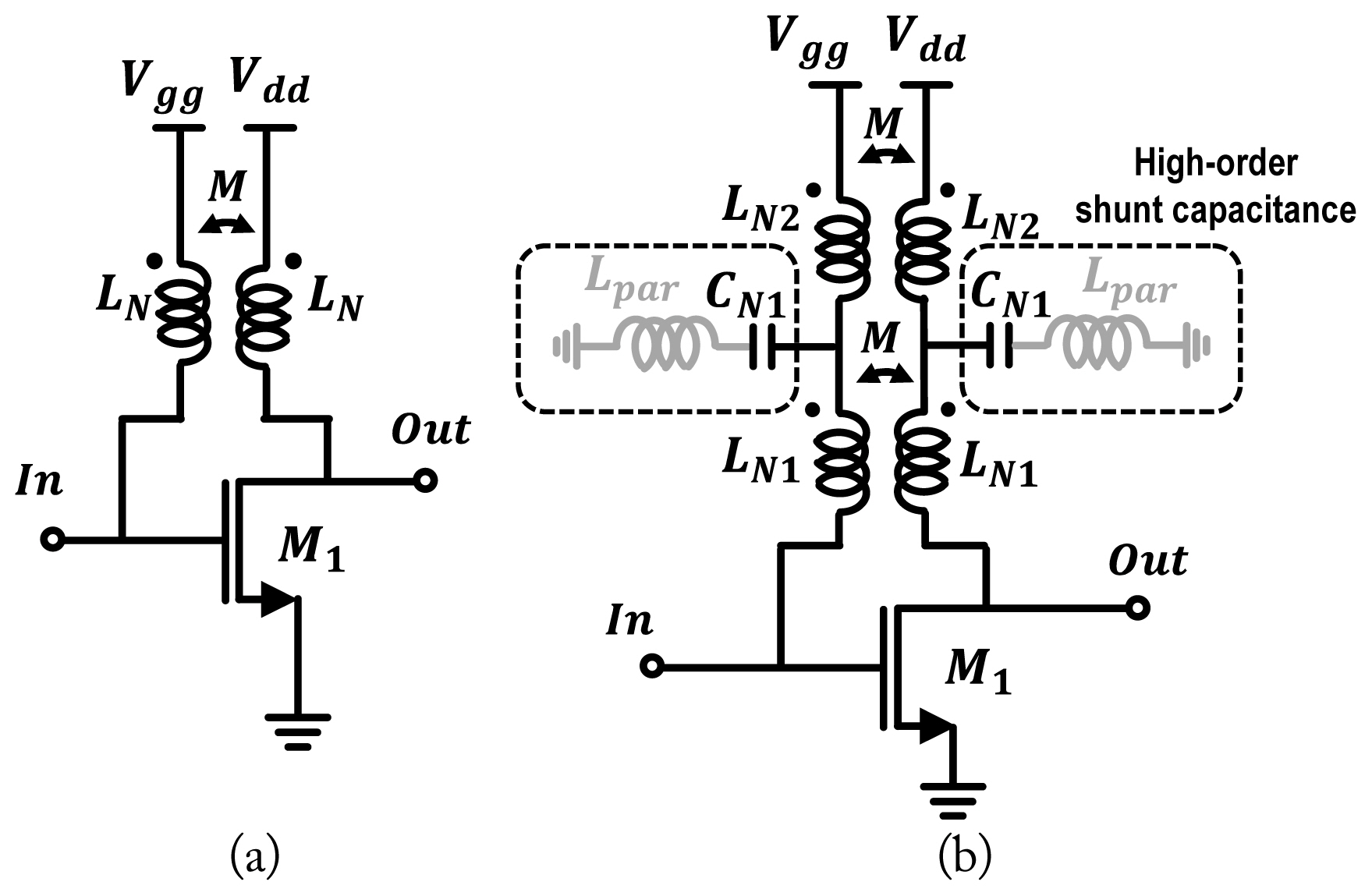
Transformer-based neutralization circuit: (a) single-band and (b) dual-band application.
Thus, the simple coupled-line parameters of a transformer-based network can neutralize Cgd at the operation frequency. Single-band neutralization can be implemented as a simple first-order circuit, as shown in Fig. 1(a). However, for dual-band operations in the proposed LNA, the order of the neutralization network must be raised above the third order, which requires a high-order shunt capacitance, as shown in Fig. 1(b).
To realize the dual-band operation, the related matrix, equations, and the equivalent circuit shown in Fig. 2 are expressed in the transformer-based neutralization network, and those equations are well known as follows [8]. First, to simplify the transformer-base neutralization circuit analysis, the equivalent circuit components are assumed symmetric, LN1 = LN2 = LN, respectively. As shown in Fig. 2, the transformer-based neutralization network is composed of two coupled lines and a high-order shunt capacitance. They assume that the input voltages and currents are V1, V2, I1, I2, I3, and I4, respectively. The admittance parameter (Y-parameter) is used for analytical equation derivation owing to the one-stage of the LNA. For the reverse admittance derived, voltage, and current relation described, the overall input–output relation can be derived as follows:
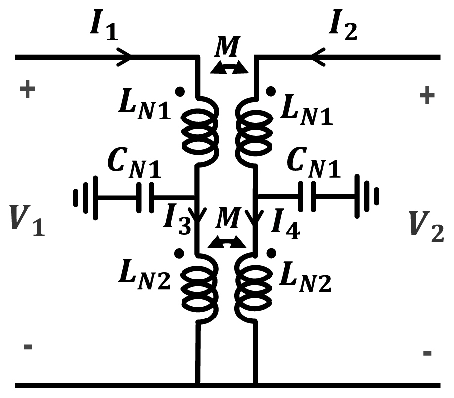
Transformer-based neutralization equivalent circuit: dual-band application.
The reverse admittance Y12=I1/V2|V1=0 is defined by detail expression as below:
From the neutralization condition Y12−sCgd = 0 (1), it can be rewritten as follows:
Near the transformer relation Leq = LN2/M−M,
Again, letting S=jω, and to simply, since
Assuming that ω0=ωN, the six-order polynomial equation can be rewritten as follows:
From the equation, its roots can be generalized as follows:
Now, by solving the six-order equation derived from the neutralization condition of the transformer-based neutralization equivalent circuit, we can obtain three positive solutions. The first two solutions, denoted as ωBand_L and ωBand_H, are located close to each other within the W-band of each band, while the last root, ωBand_3, is located out of the band. These three roots indicate that a simple transformer-based neutralization network consisting of two coupled lines and a high-order shunt capacitance can achieve neutralization at each band. Details are provided below:
Thus, implementing high-order shunt capacitance for dual-band operation is an important design parameter. However, in practice, parasitic inductance significantly reduces the reactance of the capacitor. As depicted in Fig. 1-(b), the following formula can be considered:
Fig. 3(a) and 3(b) show the typical and optimized layout structures, respectively, of the high-order shunt capacitance corresponding to Fig. 1(b). It comprises five components: the metal-insulator-metal (MIM) capacitor (CN1), back-via top metal (Lm1), bias to MIM metal connection (Lm3), MIM to MIM air-bridge metal (Lm2), and the back-via (LBV) structure, respectively. Note that the undesired parasitic inductances (Lpar: Lm1 + Lm2 + Lm3 + LBV) lower the Q-factor of the high-order shunt capacitance and drastically degrade the neutralization effect in the W-band.

High-order shunt capacitance structure: (a) typical layout and (b) optimized layout in this work.
First, to reduce parasitic inductances, Lm3 is included as the one MIM capacitor structure in the bias line of the neutralization network. However, Lm1 and LBV also induce undesired parasitic inductance, which makes it difficult to implement the desired small-value capacitor for high-order shunt capacitance.
Subsequently, it reduces the physical length of Lm1 to reduce Q-factor degradation. These are realized by reusing the top metal structure of the LBV for other MIM capacitor structures. The self-resonance frequency (SRF) of high-order shunt capacitance improvement and enhanced dual-band operation can be realized by reducing these parasitic inductances: (Lm1 + Lm3).
Fig. 4 shows the total parasitic inductances of the high-order shunt capacitance. In this sequence, the total parasitic inductance of the shunt capacitance is cut down from 37 pH to 23 pH in the optimized capacitance structure. Fig. 5(a) shows the Q-factor, which is enhanced over two times compared to the typical structure. Furthermore, Fig. 5(b) shows that the SRF of the optimized structure is 10% higher than that of the typical structure.

Simulation results of total undesired parasitic inductances of the high-order shunt capacitance.

Simulation results of the high-order shunt capacitance caparison: (a) Q-factor simulation results and (b) effective capacitor value including SRF.
III. Dual-Band LNA Circuit Design
Sopt and Zopt (noise and gain circles) of the process are illustrated in Fig. 6. In the design of a one-stage LNA with input/output impedance matching network, it is essential to consider the placement of input and output stability circles in order to avoid unstable circuit areas. In the case of a dual-band LNA design, the impedance at each band is positioned closely together, leading to a more favorable trade-off between amplifier noise figure, gain, and input return loss.
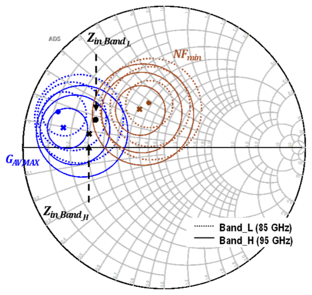
Constant noise figure circles and gain circles of a single transistor process design kit (PDK) device at 85 GHz and 95 GHz (0.2 dB steps at Vgs = −0.4 V, Vds = 1 V).
Fig. 7 shows a comparison of the simulation results between a single transistor with the proposed transformer-based neutralization network and a transistor without it. The maximum available gain (MAG) of the transistor with neutralization applied in Band_L and Band_H demonstrates improvement compared to the case without neutralization. The neutralization effectively enhanced the gain performance in the target band while exhibiting some degradation in the other band, resulting in dual-band operation, as depicted in the overall MAG plot. The minimum noise figure is a slight degradation at the target frequency bands, even with the adaption of neutralization.
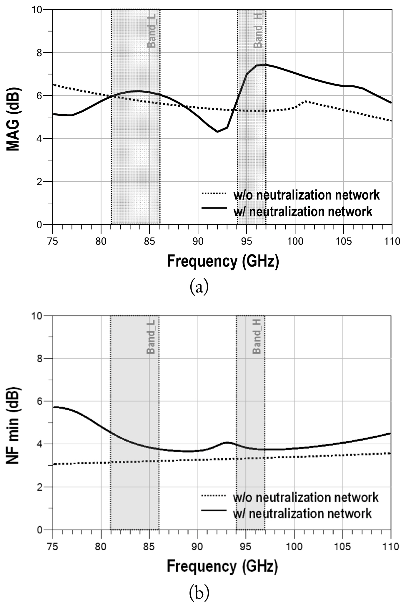
A single transistor PDK device simulation results: (a) maximum available gain plot and (b) minimum noise figure.
The four-stage cascade LNA structure was designed using a high-order transformer-based neutralization structure, as shown in Fig. 8. In the first stage, peak gains of 4.4 dB and 4.9 dB and noise figures of 3.7 dB and 3.8 dB are achieved in the lower-and upper-frequency bands (Band_L, 81–86 GHz; Band_H, 94–97 GHz), respectively. The subsequent stage is matched for the small noise contributions and optimized for each stage. The transformer-based neutralization network realized the gate and drain bias lines of the transistors by reusing them to reduce the chip area. The input and output matching networks were designed with a transformer structure and an open stub. As a simulation result, a four-stage LNA had a peak small-signal gain of 18.8 dB and 21.9 dB at the lower- and upper-frequency bands (at 84 and 96 GHz, respectively). The noise figures are 4.5 dB and 4.3 dB at each lower- and upper-frequency band. The transistor size is 2 × 25 μm at each stage. Capacitors were implemented by the MIM structure configuration, and the LBV structure described the GaAs process.

Schematic of the optimized four-stage LNA with transformerbased neutralization technique.
IV. Measurement Results
To verify the optimized neutralization technique, the W-band dual-band LNA was realized using a 0.1-μm GaAs pHEMT process with a 100-μm thick substrate. The chip photograph is shown in Fig. 9, with an overall chip size of 2.17 mm2, including the pads. A four-stage cascade LNA was measured using an on-wafer probe condition with W-band frequency extender modules.

Chip photograph of the dual-band LNA (chip area 1,550 × 1,400 μm2, including pads).
Fig. 10 shows that the small signal gains are 20.3 dB and 21.7 dB at the lower- and upper-frequency bands, respectively. The measured input and output return losses were greater than 4 dB and 10 dB, respectively, in the overall bands, demonstrating broadband output matching. The noise figure was also measured using a noise figure analyzer (Keysight N8975A), a W-band block-down converter, and a W-band waveguide noise source (NoiseCOM NC5110A). The measured noise figures were 5.0 dB and 6.4 dB in the lower- and upper-frequency bands, respectively (Fig. 11). All passive components and structures were designed and optimized using an electromagnetic momentum simulation environment. The total drain current was 46 mA with 1 V VDD.
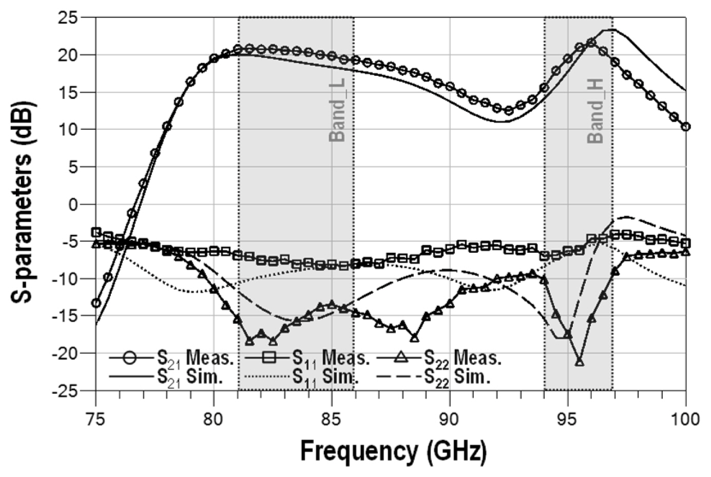
On-wafer measurement results of the S-parameters.

On-wafer measurement results of noise figure.
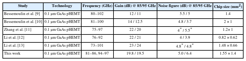
Table 1 summarizes the performance comparison of the W-band LNAs. This is compared to the results of a broadband LNA implemented in a GaAs pHEMT [9–13]. The various GaAs pHEMT W-band LNAs can be attributed to broadband topology. The measured dual-band LNA showed a similar performance as [10].
Performance comparison of the W-band LNA MMICs
In this work, the parasitic inductances of high-order shunt capacitance were minimized by reusing the transistors’ bias lines as one capacitor and the top metal of the back via another capacitor. As a result, a high-Q transformer-based neutralization network was realized to connect each transistor structure, enhancing performance degradation in the W-band. Even though the performance was not superior to that of the broadband technique, the rejection of undesirable bands was observed in contrast to the broadband LNAs. Moreover, this is the first study that has attempted dual-band LNA among W-band GaAs pHEMT LNAs.
V. Conclusion
A dual-band LNA in the W-band was realized using an enhanced Q-factor transformer-based neutralization network with a gate-drain line feedback structure. The fabricated W-band dual-band LNA achieved dual-band LNA covering these two W-band frequency bands (Band_L, 81–86 GHz; Band_H, 94–97 GHz). Thus, dual-band LNA can be a competitive architecture in a W-band cooperative joint communication and radar application system.
Acknowledgments
This work was supported by the Agency for Defense Development (Contract No. UG200003ED).
References
Biography

Taejoo Sim, https://orcid.org/0000-0003-1474-4310 was born in Changwon, South Korea, in 1994. He received his B.S. degree in electrical engineering from Hanyang University, Ansan, South Korea, in 2019, and is currently working toward a Ph.D. His current research interests include monolithic micro-wave integrated circuit design for microwave and millimeter wave power amplifiers and low noise amplifiers using gallium nitride high electron mobility transistor (GaN HEMT) and gallium arsenide pseudomorphic high electron mobility transistor (GaAs pHEMT) processes.

Dongmin Lee, https://orcid.org/0000-0003-2687-6126 was born in Daegu, South Korea, in 1995. He received his B.S. and M.S. degrees in electrical engineering from Hanyang University, Ansan, South Korea, in 2020 and 2022, respectively. Since 2022, he has been working at the MMII Laboratory Corporation, an RF front-end IC design house in South Korea, where he is currently involved in the development of millimeter wave ICs. His current research interests include monolithic microwave integrated circuits (MMICs) design for microwave and millimeter wave power amplifiers using gallium nitride high electron mobility transistor (GaN HEMT), gallium arsenide pseudomorphic high electron mobility transistor (GaAs pHEMT), and silicon germanium bipolar complementary metal oxide semiconductor (SiGe BiCMOS) processes and modeling of millimeter wave package substrates.

Wansik Kim, https://orcid.org/0000-0002-2198-8754 received his B.S., M.A., and Ph.D. degrees from Konkuk University, Seoul, South Korea, in 1991, 1993, and 2005, respectively, all in electrical and electronics engineering. In 1999, he joined the Institute for Advanced Engineering in Yongin, South Korea, where he was involved in the development of millimeter-wave transceiver systems for FMCW radar. Since 2005, he has been with the Radar Research and Development Center, LIG Nex1 Company Ltd., South Korea, where he is currently involved in the development of transceiver systems for FMCW radar. His research interests include integrated circuits and systems from X-bands to millimeter-waves.

Kichul Kim, https://orcid.org/0000-0003-1652-5576 was born in Daegu, South Korea, in 1981. He received his M.S. degree in electrical engineering from Gwangju Institute of Science and Technology (GIST), Gwangju, Korea in 2011, and a Ph.D. degree in electrical engineering from the Korea Advanced Institute of Science and Technology (KAIST), Daejeon, Korea, in 2016. From 2007 to 2008, he worked with Samsung Thales, Yongin, Korea. In 2016, he joined the Agency for Defense Development (ADD), Daejeon, Korea. His research interests are RF integrated circuits, RF components, and communication systems.

Jeung Won Choi, https://orcid.org/0000-0002-3642-2323 was born in Daejeon, South Korea, in 1966. He received his B.S. and M.S. degrees in Computer Science and Statistics from Chungnam National University, Deajeon, South Korea, in 1989 and 1993, respectively, and his Ph.D. in Computer Science from Chungnam National University, Deajeon, South Korea, in 1997. In 1997, he joined the Agency for Defense Development (ADD), Daejeon, South Korea, where he is currently a principal researcher. In 2013, he joined the Department of Weapon System Engineering from the University of Science and Technology, Daejeon, South Korea, as a faculty member, where he is currently a professor. His research interests are tactical communication, satellite communication, cognitive radio, RF components, and global position systems.

Min-Su Kim
https://orcid.org/0000-0002-7566-5408 was born in Seoul, South Korea, in 1978. He received his B.S. degree in electronic engineering from Incheon University, Incheon, South Korea, in 2005, and M.S. and Ph.D. degrees in information and communication engineering from Sungkyunkwan University, Suwon, South Korea, in 2008 and 2012, respectively. From 2012 to 2015, he worked with Samsung Electronics, System-LSI Business, Giheung, South Korea, where he designed receiver circuits for transceivers in mobile terminals. From 2015 to 2018, he was with Broadcom Inc., where he designed low-noise power amplifiers for various LNA-PAMiDs. Since March 2022, he has been with the Department of Information and Electronic Engineering, Mokpo National University, Muan, South Korea, where he is currently an assistant professor. His research interests include low-noise amplifier design, power amplifier design, RF integrated circuit (IC) design, and mm-wave IC design for RF systems.

Junghyum Kim
https://orcid.org/0000-0001-9424-3377 was born born in Busan, South Korea. He received a Ph.D. degree in electrical engineering from Seoul National University, Seoul, South Korea, in 2005. In 2000, he was a student co-founder of WavICs—a power amplifier design company, which is now fully owned by Broadcom—where he invented the switchless stage-bypass power amplifier architecture called CoolPAM. From 2005 to 2007, he worked with the Wireless Semiconductor Division at Avago Technologies, as a group manager of the Integrated Circuit Design Group. In 2007, he joined the Division of Electrical Engineering, Hanyang University, Ansan, South Korea, as a faculty member, where he is currently a professor. From 2007 to 2018, he was an external director with Broadcom. He holds more than 60 U.S. patents on power amplifier technology and RF integrated circuits. His current research interests include monolithic microwave integrated circuit design for mobile communication and millimeter-wave systems, thermal packaging analysis of high power devices, and intermodulation and noise analysis of nonlinear circuits.