


I. Introduction
The sub-THz band is a strong candidate for the frequency region of next-generation mobile communication because it can utilize a wider frequency band than previously developed mobile communication systems. However, addressing the substantial path loss associated with sub-THz band communication is a crucial challenge. By adding an amplifier to the sub-THz band wireless link, for example, at the input port to the receiver or the output port to the transmitter, we can compensate for the large path loss.
Most sub-THz band amplifiers are being developed based on monolithic microwave integrated circuit (MMIC) technology. Notably, to use an amplifier in communication systems, it is necessary to modularize the amplifier or integrate it with other components.
There have been many efforts to build integrated systems for sub-THz applications [1ŌĆō4]. Integrated systems operating in the sub-THz range have size advantages due to the reduction in the size of passive components and antennas as the frequency increases. In mass production, it is cost-effective to manufacture chips using CMOS-based processes. However, for sub-THz frequency amplifiers, amplifiers developed using IIIŌĆōV-based processes demonstrate higher maximum output power, gain, and wider bandwidth performance than those developed using CMOS-based processes [5ŌĆō7]. Therefore, for sub-THz amplifiers, it is advantageous to explore the development of amplifiers using IIIŌĆōV-based processes.
IIIŌĆōV technology amplifiers need to be connected with subcomponents from other technologies for system-level applications. Achieving a high-performance amplifier often necessitates the separation of the amplifier chip from other subcomponents, even when they are developed using the same process as the amplifier, due to variations in IIIŌĆōV fabrication. However, in such cases, it is essential to establish connections between the amplifier and subcomponents. There are several methods available for transferring sub-THz signals from a chip to other components in order to connect sub-THz components. For instance, IIIŌĆōV-based chips can be connected with chips from other technologies using the chip-on-board (COB) technique. To establish the connection of sub-THz signals between chips, wire bonding, which is traditionally used, can be employed. However, as the frequency increases due to the impedance of the wire, the signal attenuation becomes significant. In [8], up to 6 dB of loss was observed in the J-band. The flip chip approach exhibits wideband characteristics from DC to high frequencies and shows low losses of around 0.9 dB at 500 GHz [9], but its fabrication costs are high, making it difficult to implement. In addition, some studies have explored high resistivity lenses [10, 11] or small horn antennas together during the COB process [12, 13] to directly radiate the sub-THz signal into the air. However, there may be alignment issues leading to beam direction deviation, and further research is required to acquire higher directivity to compensate for the high path loss at sub-THz frequencies.
Besides COB, a building waveguide module using a split block is a widely employed method in high-frequency bands. The development of waveguide modules offers several advantages, primarily due to their high compatibility with various other waveguide components. Many sub-THz components, such as antennas, uni-traveling-carrier photodiodes (UTC-PDs), mixers, and sources, have been developed in the form of waveguide modules. Waveguides offer low loss and wide frequency band characteristics, resulting in negligible attenuation and minimal impact on the frequency response of a circuit. Furthermore, the use of waveguides allows for the making of a sturdy module with excellent heat dissipation. In particular, the use of an E-plane probe is a common method for converting the quasi-TEM mode on the substrate into the TE10 mode in the waveguide. The E-plane probe is designed for single-ended input and output and offers advantages such as wide operating bandwidths and low insertion loss. However, the input and output of packaging are typically not aligned in-line. E-plane probes in various forms have been proposed, including rectangular poles [14, 15] and radial probes [16]. Waveguide transitions using the end-wall have also been reported in the sub-THz range [17, 18]. The end-wall method involves arranging the normal vector of a microstrip patch perpendicular to the direction of the electromagnetic waves in the waveguide. Unlike the E-plane probe method, it has the advantage of not requiring a quarter-wavelength metal short block [19]. Dipole transitions are another form of waveguide transition. Similar to the E-plane probe, the pole of the dipole transition is aligned perpendicular to both the direction of the electromagnetic waves and the E-field, but the signal in the quasi-TEM mode is differential. Unlike the E-plane probe, where the pole is in the same direction as the transmission line, the pole of the dipole transition is perpendicular to the direction of the transmission line. Chips that use the dipole transition have input/output signals aligned in-line by default. Dipole transitions have the advantage of minimizing substrate losses by reducing the width of the substrate around the dipole. A ridge structure is also used for waveguide transition. This requires installing ridges near the transmission lines inside the waveguide to gradually match the EM field of the waveguide and the transmission line [20], and this technique has been employed by NTTŌĆÖs 300-GHz-band communication system [21]. In this research, a dipole transition that allows for a smaller chip area while being easily applicable to differential circuits is utilized.
Given that the wavelength in the sub-THz band is shorter than 1 mm, even minor errors in the order of several tens of micrometers during the module assembly process can significantly affect the characteristics of the waveguide transition. In this study, we investigated the impact of packaging on amplifier module performance with electromagnetic (EM) simulations for successful amplifier module packaging. In particular, we focused on developing the module such that no undesired modes occurred during the modularization of the chip. When an undesired mode occurs, the amount of signal transmitted through the chip at the frequency where the mode occurs decreases, and the gain of the amplifier module also decreases at that frequency. This results in poor frequency flatness of the amplifier module gain. Consequently, it adversely affects the overall frequency flatness of the system. In wireless transmissions, non-flat frequency response characteristics can lead to the loss or distortion of signal frequency components. Ultimately, this degradation can impact the bit error rate (BER). Furthermore, when the undesired mode occurs, the return loss of the module decreases at the corresponding frequency, leading to suboptimal impedance matching with other components. This can cause standing waves that interfere with the signal, leading to signal distortion, jitter, and a reduction in the signal-to-noise ratio (SNR). In addition, we successfully demonstrated sub-THz band wireless links operating at carrier frequencies of 281 GHz and 288 GHz, leveraging photonics technology and using the amplifier module we developed.
II. Design of Amplifier Module
A three-stage differential cascade amplifier chip, based on a 250-nm indium phosphide (InP) double heterojunction bipolar transistor (DHBT) process, was packaged inside a gold-plated aluminum split block. The signals between the amplifier chip and the waveguide are coupled through dipoles located at the input and output of the amplifier chip.
1. Waveguide Transition
Fig. 1 shows the structure of the waveguide transition designed on a 75-╬╝m-thick InP substrate with a 6.8-╬╝m-thick benzocy-clobutene (BCB, ╔ør = 2.7) layer. The ground plane and dipoles were designed using M1 and M4 metal layers, respectively. The backside vias were densely arranged between the bottom of the InP and M1 metals to suppress the substrate mode. The waveguide size was in line with the WR3.4 standard. In Fig. 1, w1 is the width of the chip, l1 is the distance between the dipole and the chip edge, and s1 and s2 are parameters indicating the gap between the chip and one sidewall of the split block. The parameter values determined by the simulation are shown in parentheses.
In the design of the waveguide transition, errors of several tens of micrometers may occur during split block machining, chip cutting, and chip attachment. For this reason, it is necessary to find designed values that are not sensitive to change or a method to reduce the influence of assembly errors. The single waveguide transitions were simulated by controlling the values of parameters related to chip cutting and alignment to analyze possible errors during the packaging process. Fig. 2 shows the simulation results, and the values in Fig. 1 are applied to other values that are not varied in the simulation.
It can be seen from Fig. 2(a) that the waveguide transition has the lowest sensitivity to parameter changes at w1 of 420 ╬╝m. However, w1 was designed to be 430 ╬╝m due to design rule checking (DRC). If the value of w1 is greater than 440 ╬╝m, the reflection loss is lowered to 10 dB or less at the frequency of interest, an undesired mode occurs, and the insertion loss is increased to a value exceeding 1 dB. In this case, the undesired mode arises due to the concentration of energy between the M1 ground metal edge and one side of the split block region. Moreover, chips with larger w1 values are difficult to assemble. Therefore, the chip was scribed so that w1 was as small as possible, and chips with a large w1 were excluded.
For the l1 value with a range of 10ŌĆō50 ╬╝m, the shorter the l1, the higher the operating frequency band and the larger the return loss, but the bandwidth decreases (Fig. 2(b)). For packaging, a value of 30 ╬╝m was applied to l1. The chip cutting error is about 20 ╬╝m, and if l1 is 30 ╬╝m, even assuming the maximum error, the possible return loss is more than 10 dB. Furthermore, the operating frequency band can be assured at 250ŌĆō320 GHz based on an insertion loss of 1 dB. The simulated minimum insertion loss of a single waveguide transition is about 0.4 dB. To minimize any impact on the 3-dB bandwidth of the amplifier, a frequency bandwidth assessment was conducted based on a 1-dB insertion loss criterion.
In Fig. 2(c), the bandwidth became narrower, and the flatness of the insertion loss deteriorated as s1 and s2 were beyond the value of 10 ╬╝m. With s1 = 2 ╬╝m and s2 = 8 ╬╝m, as shown in Fig. 2(c), the characteristics of the waveguide transition degraded at specific frequencies due to the asymmetric formation of the E-field between the two poles that constituted the dipole. This asymmetry was caused by the chip being misaligned at the center of the waveguide. Therefore, to reduce the misalignment of the chip, the values of s1 and s2 were checked microscopically during assembly.
The assembly of the chip at an angle can result in impaired signal transmission characteristics. Fig. 3 depicts the structure of the waveguide module used to examine the effect of a chip alignment angle error. In Fig. 3, two chip-to-waveguide transitions are connected back-to-back using a 100-╬® differential line, which is approximately 1 mm in length. The length of the line is determined based on the size of the amplifier chip that will be used in the waveguide module. Fig. 3(b) shows a top view of the chip placement on the xy-plane. To simplify the simulation configuration, the center of the chip and the waveguide split block are placed at the origin O of the coordinate system, and the rotated angle of the chip with respect to the origin O is denoted as ╬Ė.
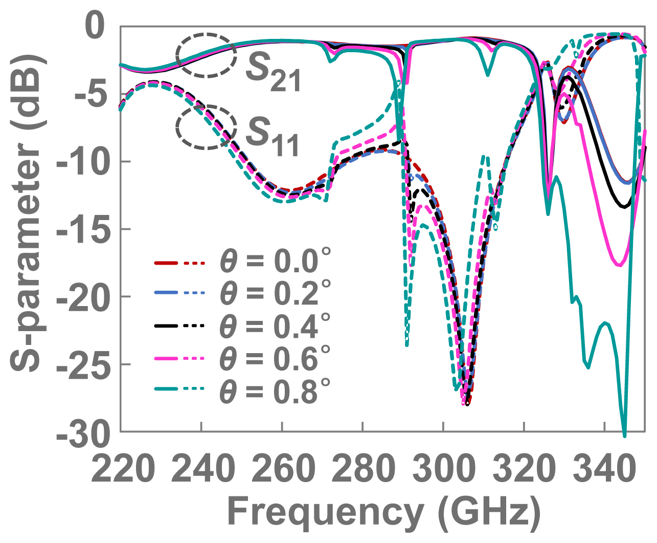
The simulation results of the chip alignment angle error are illustrated in Fig. 4. Due to the extremely narrow spacing of 10 ╬╝m between the chip and one sidewall of the split block, it was only possible to vary the value of angle ╬Ė up to a maximum of 0.8┬░. As ╬Ė increased, near specific frequencies, such as 265, 289, and 312 GHz, the magnitude of S21 decreased and matching degraded. At 289 GHz, which is shown as the worst case in Fig. 4, Fig. 5 compares the E-field intensities in the waveguide module shown in Fig. 3 for two different angles, ╬Ė = 0┬░ and ╬Ė = 0.8┬░. Even a slight deviation in the angle between the dipole radiator and the center of the waveguide can cause distortion in the direction of wave propagation and disrupt EM field symmetry inside the waveguide. The graph in Fig. 5 for ╬Ė = 0.8┬░ shows a concentration of E-field on one side of the pole of the dipole, which can result in differences in signal strength between the lines connected to the poles. Angle errors can be more problematic for differential circuits. Furthermore, as shown in Fig. 5, when ╬Ė = 0.8┬░, the E-field is spread over a wider area and is not concentrated near the signal path, unlike in the case when ╬Ė = 0┬░. This means that, at this frequency, the absorption of the waveguide signal by the dipole is less when the chip is misaligned in angle than when it is correctly aligned. During assembly, it is crucial to exercise caution to prevent any misalignment of the chip. To minimize errors in angle ╬Ė, we also performed microscopic checks.
To mitigate potential problems during the packaging of waveguide modules, it is important to verify and address any production errors in the split block. It is also important to design relevant physical parameters to ensure the waveguide transition exhibits the most stable characteristics. Furthermore, during module production, it is necessary to carefully select chips that have been precisely cut according to specifications and use a microscope to ensure proper chip alignment by comparing the chip attachment area before and after chip attachment.
2. Bondwire Passage
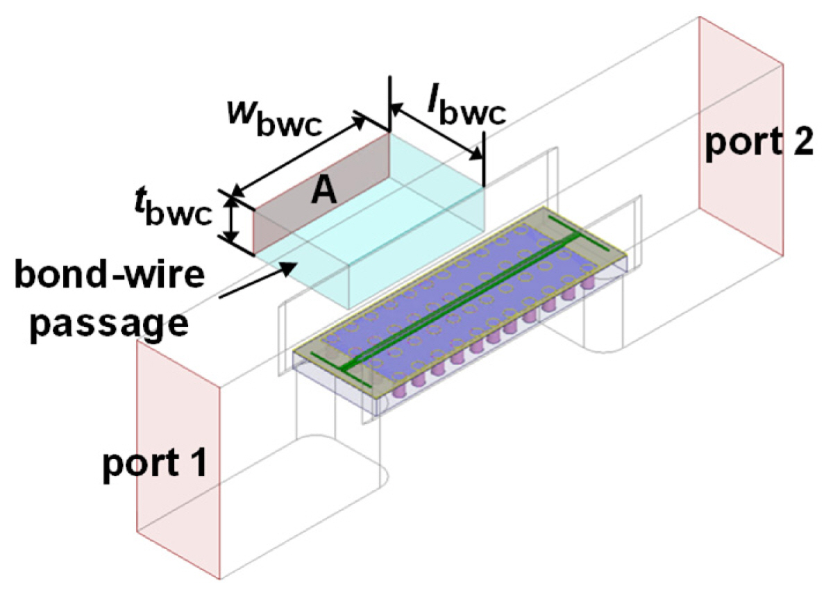
Bondwires were used to connect the chip with an external circuitry, such as a bias board. It is important to note that the bondwire passage, the space in which the bondwires are located, affects the transfer characteristics of the waveguide module. The structure is the same as in Fig. 3 with ╬Ė = 0┬░, except for the bondwire passage. Beyond surface A in Fig. 6, there is a large space for the external circuit; therefore, surface A can be considered a radiation boundary. Herein, wbwc, lbwc, and tbwc are the width, length, and thickness of the bondwire passage, respectively. Fig. 7 shows a simulated E-field intensity in that structure when the TE20 mode is generated in the bondwire passage and the transfer characteristic is severely degraded. A bondwire passage of a chip with a large number of DC pads can be designed, as shown in Fig. 7. Determining the appropriate bondwire passage size is also a consideration in amplifier module packaging.
A bondwire passage can be conceptualized as a rectangular waveguide, and its size can be determined using the cutoff frequency (fc) of the rectangular waveguide. The cutoff frequency (fc) of the waveguide The cutoff frequency (fc) of the waveguide is determined by (1) [22].
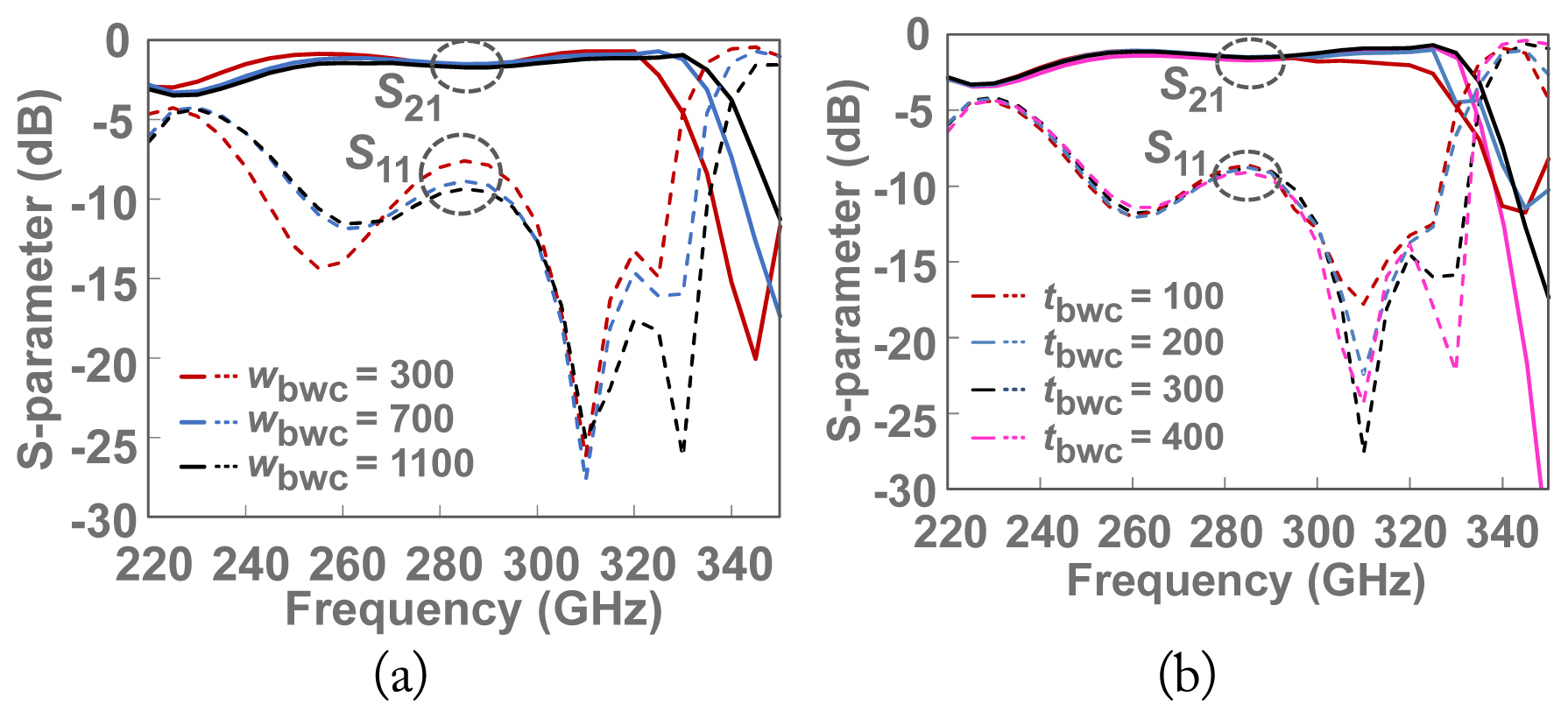
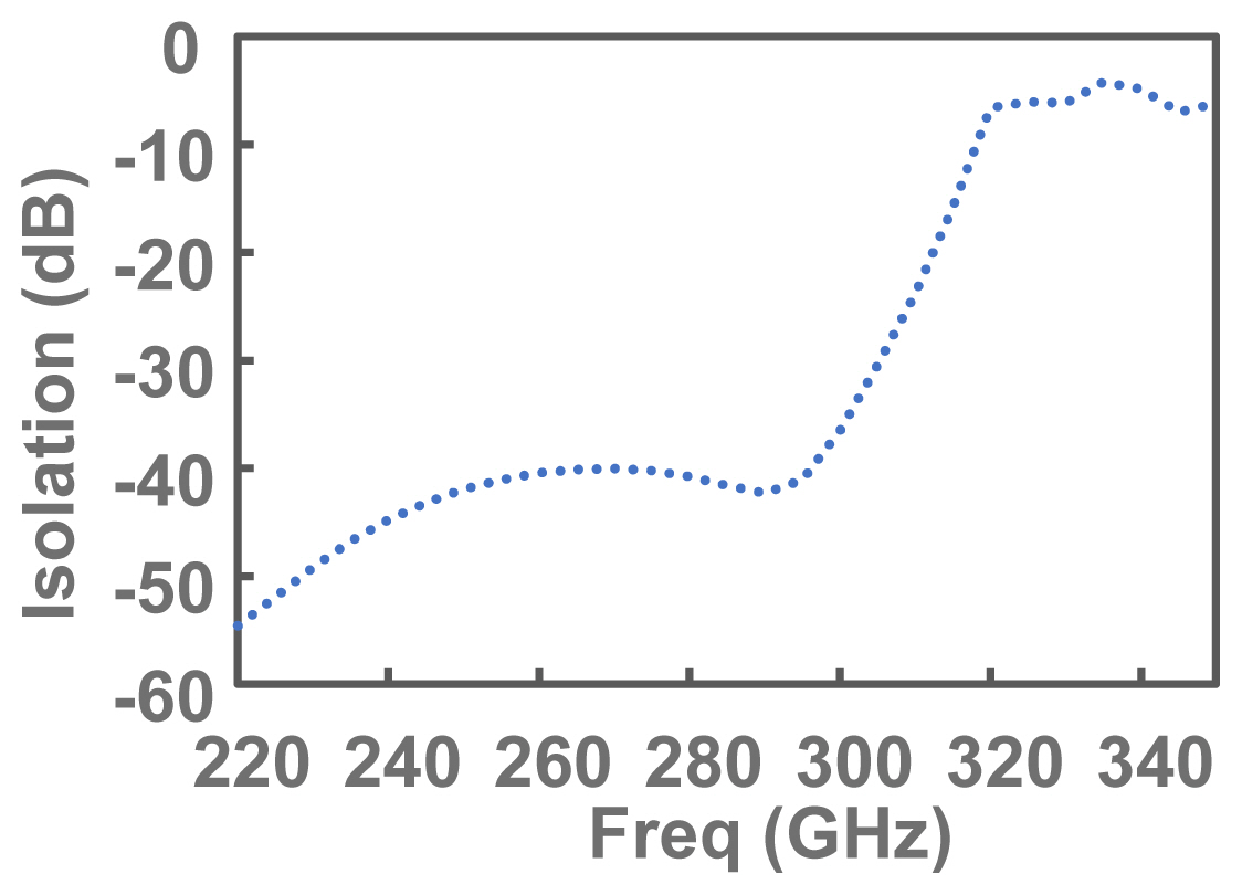
where c is the speed of light, a is the width of the waveguide, b is the height of the waveguide, and n and m indicate wave modes. In the TE10 mode, which is the dominant mode in a rectangular waveguide, fc is calculated as 300 GHz with a = 500 ╬╝m. It can be inferred that the width of the bondwire passage should be 500 ╬╝m or less to block the signals transmitted from the waveguide to the bondwire passage. However, the calculated bondwire passage space is not suitable for the amplifier module in this study. The chip requires three DC biases, and a 600-╬╝m-wide single-layer capacitor (SLC) is connected to the DC pads. A bondwire or bonding tip may interfere with the split block with a 500-╬╝m width bondwire passage. In addition, using Eq. (1), it is not possible to predict that an undesired mode will occur, as shown in Fig. 7. In order to design the bondwire passage as large as possible, an EM simulation was performed while changing the width and thickness tbwc, and the results are presented in Fig. 8. The simulations in Fig. 7 confirm that modes occur at the bondwire passage when wbwc = 1,100 ╬╝m and tbwx = 100 ╬╝m, which indicates a wide and flat bondwire passage. Additional simulations were conducted by decreasing the value of wbwc and increasing the value of tbwx from the initial parameters (wbwc = 1,100 ╬╝m and tbwx = 100 ╬╝m). The simulations showed that modes did not occur at the bondwire passage within the simulation range. The length lbwc was fixed at 400 ╬╝m. As shown in Fig. 8, even if the width of the bonding passage is greater than 500 ╬╝m, as calculated in (1), deterioration of the waveguide transition characteristic is not observed; rather, the operating frequency band is slightly increased. If undesired modes are not formed inside the bondwire passage, most of the signals input through the waveguide are absorbed by the dipole, and the amount of signal loss due to the bondwire passage is small. Based on the simulation results shown in Fig. 8, wbwc = 700 ╬╝m and tbwc = 300 ╬╝m were determined as the passage size values. Fig. 9 shows the results of simulating the isolation between port 1 and port 2 in Fig. 6 by cutting the middle of the differential line and attaching a 100-╬® termination to the end of each differential transmission line. It shows more than 35 dB of isolation up to 300 GHz, and the structure in Fig. 6 is suitable for the amplifier module.
As explained above, determining the approximate size of the bondwire passage with Eq. (1) and performing EM simulations of the back-to-back waveguide transition containing the bondwire passage are useful for designing waveguide modules of the chip that require wire bonding. These EM simulations help ensure that undesired modes are prevented and that the transmission characteristics of the entire module structure are adjusted to closely match those obtained through the EM simulation of the single transition.
III. Experiment Results
1. Waveguide Transition
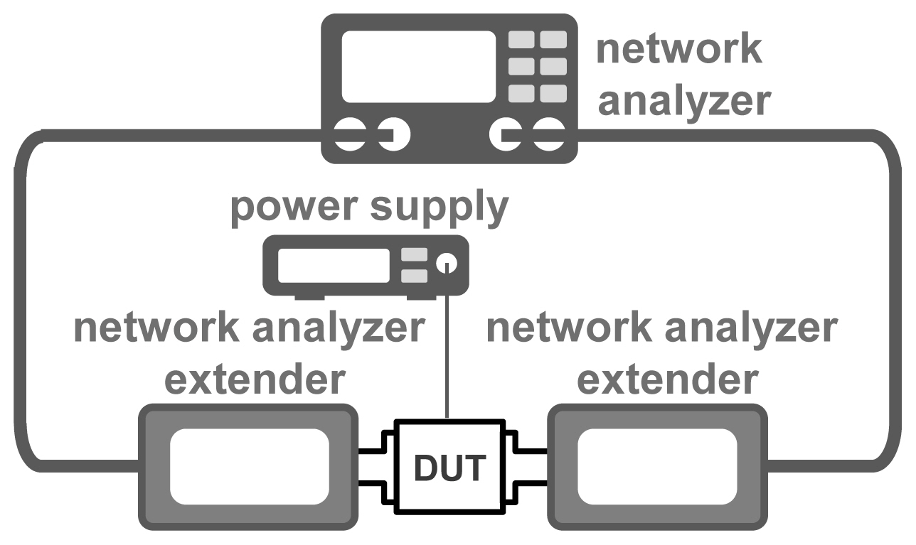
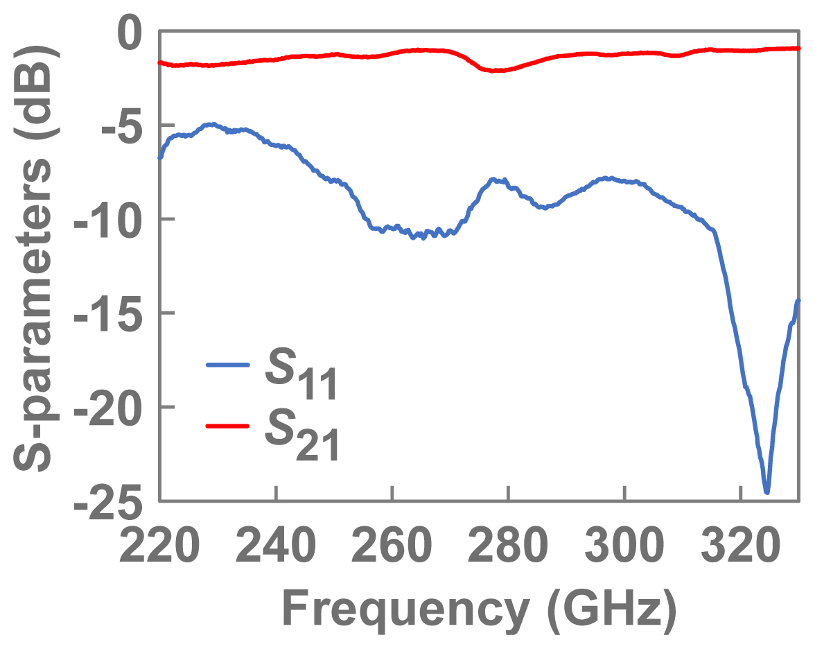
Fig. 10 displays the measurement setup used to examine the S-parameters of the waveguide module. For this purpose, VDIŌĆÖ vector network analyzer (VNA) extenders were connected to KeysightŌĆÖs VNA. Fig. 11 presents the measured and calibrated characteristics of the waveguide transition using a chip with two waveguide transitions connected back-to-back, and insertion loss was 0.9ŌĆō2.1 dB. Compared with the simulation results in Fig. 8, the return loss is similar, and the insertion loss increases in the entire frequency band. In the EM simulation, it is assumed that there is no loss due to the metal material. However, the actual metal surface is not smooth, and the loss is caused by the metal material properties, so it is thought that the insertion loss increases compared to the simulation. In Table 1, we compare various chip-to-waveguide transitions implemented on InP, quartz, and Si substrates [15, 17ŌĆō19, 23ŌĆō26]. These transitions, including the type of dipole, E-plane probe, end-wall, and ridge, operate in the sub-THz band and typically exhibit around 1 dB of insertion loss and more than 10 dB of return loss. The dipole transition presented in this manuscript has a similar insertion loss to previously published transitions but a lower return loss of 5 dB or more. Since the transitions in this manuscript operate at a wide bandwidth of over 110 GHz, except for the lower edge between 220 GHz and 250 GHz, they exhibit a return loss value of 8 dB or higher. This value is slightly lower than that of the other transitions.
2. Amplifier Module
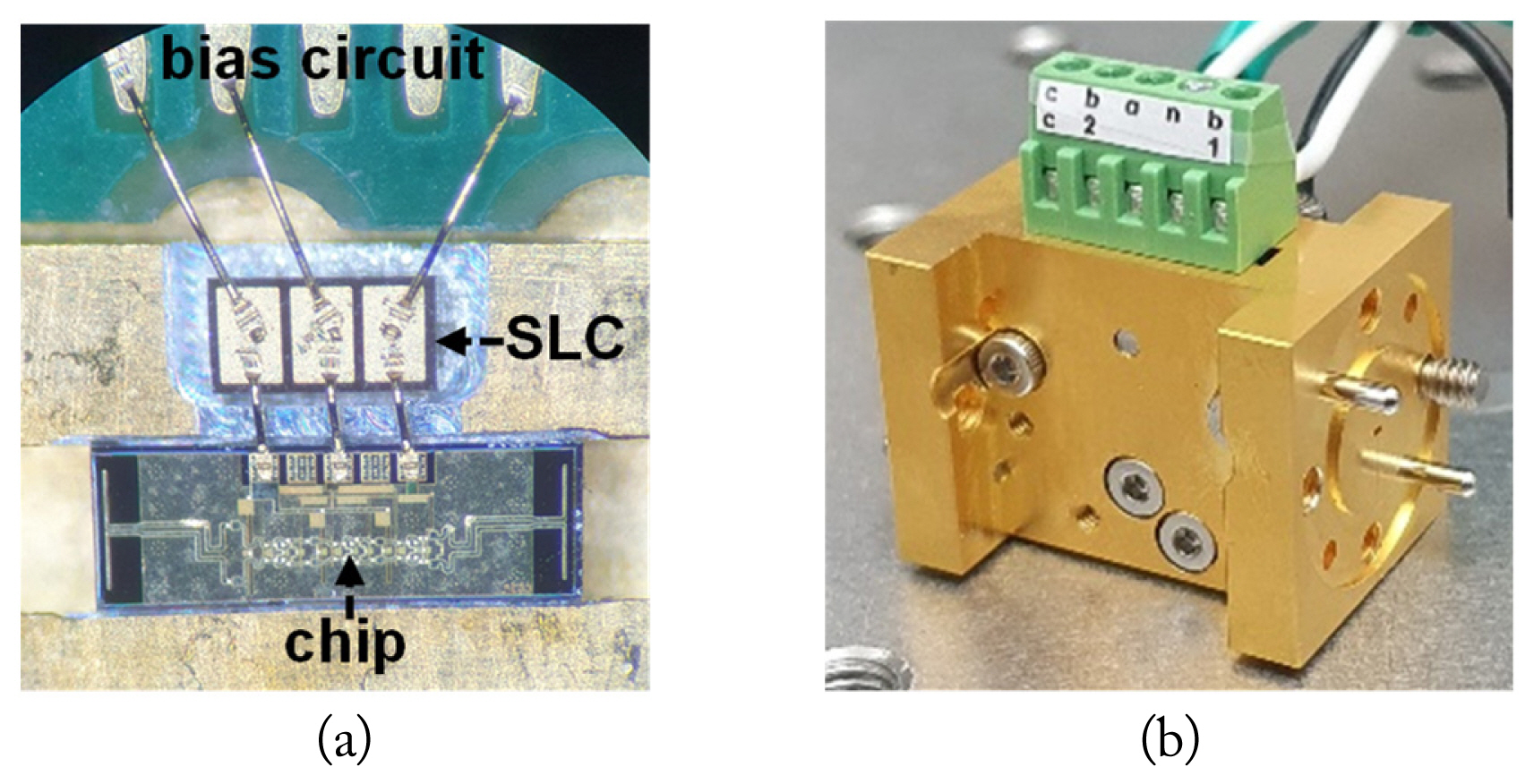
Fig. 12(a) shows a photograph of the chip attached to the waveguide module. An SLC with a capacitance of 145 fF was connected between the bias circuit and the pad of the chip. The bias circuit was designed as a low-pass filter to increase amplifier stability. Fig. 12(b) shows a photograph of the assembled amplifier module using two split blocks. To examine the characteristics of both the amplifier module and the on-chip amplifier, the measurement setup shown in Fig. 10 was used. GSG (groundŌĆōsignalŌĆōground) probes were used for the on-chip amplifier. The measurement setup shown in Fig. 10 was also used to measure the output power curve of the amplifiers. The output level of VNA port 1 was measured with a PM5 calorimeter from VDI, and the output power of port 2 was measured by varying the output power of port 1. The losses incurred by the probe were compensated.
Fig. 13 shows the measured results. The operating frequency band of the amplifier module was 257ŌĆō296 GHz, and the maximum gain was 17.3 dB at 273.5 GHz. The saturation power at 275 GHz was approximately 0.2 dBm. The 3-dB bandwidth, maximum gain, and saturation power at 275 GHz in the on-chip amplifier were 253ŌĆō290 GHz, 23.0 dB, and 4.1 dBm, respectively. The gain and saturation power were reduced by 5.7 dB and 3.9 dB, respectively, and the estimated insertion loss of the waveguide transition was 2.8ŌĆō3.9 dB. The error from the measured insertion loss (0.9ŌĆō2.1 dB) is believed to be mainly due to the difference in the gain between the two chips by process variations. In addition, the measured reverse isolation value of the amplifier module was 25ŌĆō41 dB. From these measured results, we can observe that an undesired mode does not occur, and the operating frequency band is similar to that of an on-chip amplifier even after modularization. Table 2 shows a comparison of the sub-THz amplifier modules [27ŌĆō29]. The amplifier module in this study operates at the highest operating frequency among the amplifier modules listed in Table 2 and shows the proper 3 dB bandwidth and gain performance.
3. Sub-THz Wireless Transmission with the Sub-THz Band Amplifier Module
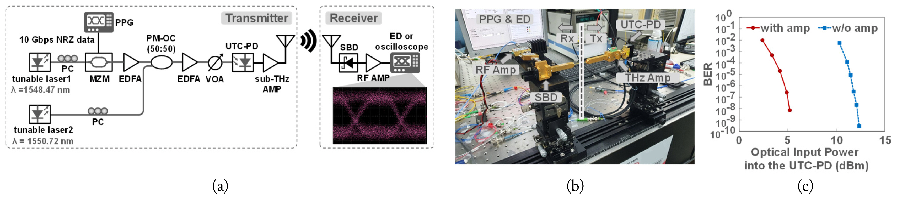
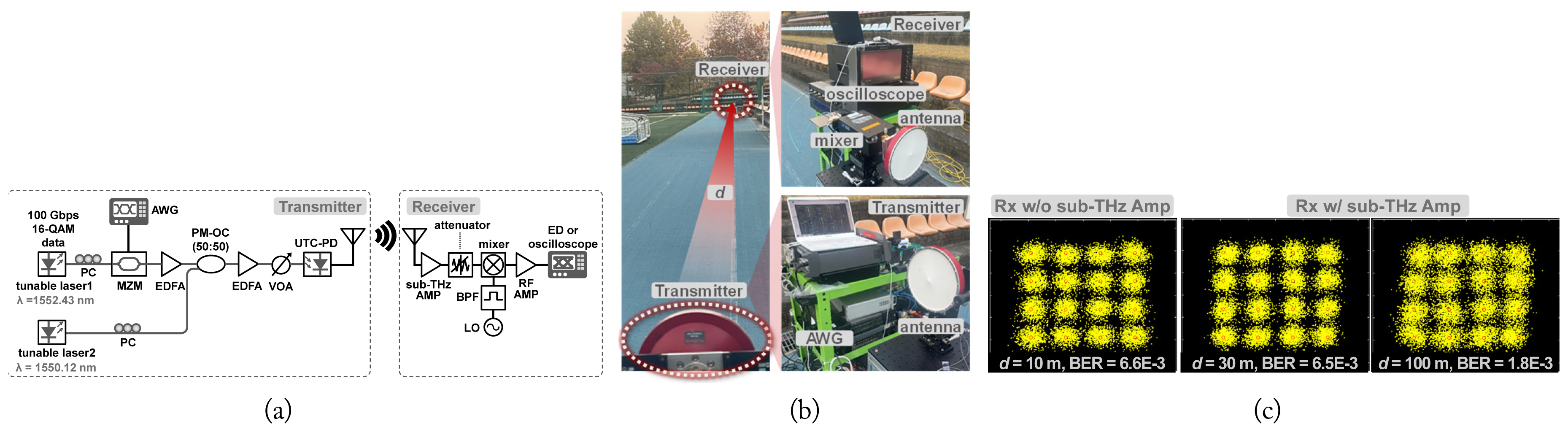
As shown in Fig. 14(a) and 14(b), the experimental setup for sub-THz wireless transmission was based on photonics [30]. The MachŌĆōZehnder modulator (MZM) was modulated with a 10 Gbps non-return-to-zero (NRZ) data stream. The wavelength of tunable laser 1 was set to 1548.47 nm. The MZM output was amplified using an erbium-doped fiber amplifier (EDFA). The wavelength of tunable laser 2 was fixed at 1,550.72 nm, and it was utilized as an optical local oscillator (LO). The wavelength difference between tunable lasers 1 and 2 was the output frequency of the sub-THz wave from the UTC-PD caused by optical heterodyne mixing. The output waveform from the UTC-PD was amplified by the sub-THz band amplifier module and subsequently radiated into the air through the horn antenna. In the sub-THz signal receiver, the baseband signal, directly detected by a Schottky barrier diode (SBD), was amplified in an RF amplifier. Finally, the received signal was analyzed using an error detector (ED) and an oscilloscope. The tunable laser is capable of generating signals with wavelengths ranging from 1,515 to 1,580 nm and has a maximum output power of 18 dBm. The EDFA operates in the C-band (1,530ŌĆō1,565 nm), with a maximum output power of 27 dBm. When 12.4 dBm of optical power is input to the UTC-PD, it produces a sub-THz signal of ŌłÆ14.4 dBm. In Fig. 14(a), the diagonal feedhorn antenna from the VDI is utilized and provides a gain of approximately 21 dB in the J-band (220ŌĆō330 GHz). Similarly, the SBD also operates in the J-band and has a typical responsivity of 1,700 V/W, along with a typical noise equivalent power (NEP) of 4.8 pW/sqrt (Hz). A photograph of the experimental setup for the sub-THz wireless transmission is shown in Fig. 14(b). Fig. 14(c) shows the measured BER with and without a sub-THz band amplifier module at a wireless transmission distance of 20 mm. With the help of a sub-THz amplifier, it was possible to reduce the optical input power into the UTC-PD by approximately 7 dB to obtain 1 ├Ś 10ŌłÆ9 BER. The sub-THz output power of a UTC-PD is proportional to the square of the optical input power. When the difference in optical input power is approximately 7 dB, the difference in output power of the UTC-PD is 14 dB, twice the previous value. The sub-THz amplifier module exhibits an average gain of 16 dB in the 265ŌĆō285 GHz frequency band, with a minimum gain of 14.2 dB. It is estimated that the optical output power increases in proportion to the gain of the amplifier module, but a slight loss of amplifier module gain is attributed to saturation effects that occur when the UTC-PD output power is high.
As confirmed by the experiment in Fig. 14, the reduction in the UTC-PD optical input was achieved by placing the sub-THz amplifier module at the output of the transmitter. However, for modulation schemes like 16-QAM that require high linearity, placing the amplifier at the output did not result in a significant increase in output power due to the linearity limitations of the amplifier. Therefore, another method is needed to transmit a signal over long distances, such as placing an amplifier at the input of the receiver. Fig. 15 depicts an experiment that successfully transmitted a 100-Gbps data rate signal with 16-QAM modulation over a long distance by positioning the amplifier module at the input of the receiver at a carrier frequency of 288 GHz. The transmitter used in Fig. 15(a) is similar to the one shown in Fig. 14(a), except for the THz amplifier module and antenna. To enable long-distance transmission, a Cassegrain antenna with a directivity of 48 dBi was employed on the transmitter and receiver. The receiver utilized a VDI mixer module with an LO multiplication factor of 12, and the intrinsic mixer single sideband (SSB) conversion loss was approximately 14 dB. An RPG level set attenuator was utilized to enhance impedance matching between the sub-THz amplifier module and the mixer. To reduce the white phase noise of the local oscillator, a bandpass filter with a bandwidth of 1.25 GHz was added to the setup. The sub-THz amplifier module employed in this experiment was assembled using the same type of circuit chip and split blocks as in the previously mentioned amplifier module. The gain of the sub-THz amplifier module shown in Fig. 15 is 16.8 dB at a frequency of 288 GHz, and the noise figure (NF) is less than 14 dB. Fig. 15(b) depicts the experimental setup, where the transmission experiments were performed by varying the distance d. Fig. 15(c) illustrates the constellation diagrams for the receiver input with and without the sub-THz amplifier module. Without the sub-THz amplifier module at the receiver input, a BER of 6.6 ├Ś 10ŌłÆ3 was obtained at a distance of d = 10 m. On the other hand, with the sub-THz amplifier module included at the receiver input, a BER of 6.5 ├Ś 10ŌłÆ3 at d = 30 m and a BER of 1.8 ├Ś 10ŌłÆ2 at d = 100 m were measured. The measured BER values satisfied the threshold for soft-decision forward error correction (SD-FEC) up to a distance of d = 100 m. The BER of 6.6 ├Ś 10ŌłÆ3 obtained at a transmission distance of 10 m without the sub-THz amplifier module is similar to the BER of 6.5 ├Ś 10ŌłÆ3 obtained at a transmission distance of 30 m with the inclusion of the sub-THz amplifier module. This suggests that the presence of the sub-THz amplifier module at the input of the receiver can compensate for the degradation in signal quality over longer distances, indicating that the use of the THz amplifier resulted in an increase in the transmission distance by approximately a factor of three. The similarity in BER values between transmitted signals indicates comparable SNRs. Taking into account the compensation for transmission distance provided by the sub-THz amplifier moduleŌĆÖs gain increase, as per the free space path loss formula, it is expected that the transmission distance will increase by a factor of seven with a sub-THz amplifier module gain increase of 16.8 dB. The increase in the total NF of the receiver would likely be the main reason for the degradation of the transmission distance. Although the estimated total NF of the receiver without the THz amplifier module at the input was below 12.3 dB, the NF of the sub-THz amplifier module was below 15 dB. This led to an overall increase in the NF of the receiver compared to when the THz amplifier was not used.
IV. Conclusion
In this study, we designed and fabricated a 250-nm InP DHBT-based sub-THz band amplifier chip. We packaged this chip within a waveguide module with optimized dimensions, including length, width, angle, and thickness. In addition, we developed a bias circuit and SLC for the packaging of the sub-THz band amplifier. Our developed amplifier module exhibited an operating frequency range of 257ŌĆō296 GHz, a maximum gain of 17.3 dB, and a saturation power of 0.2 dBm. In addition, it was confirmed that the developed amplifier module demonstrated excellent frequency flatness, making it well-suited for use in sub-THz-band communication systems. Furthermore, we successfully transmitted a 10-Gbps NRZ-modulated sub-THz signal using our amplifier module and a sub-THz transmitter based on photonics. By placing the amplifier module at the transmitterŌĆÖs output, the optical input power in the UTC-PD was reduced. Similarly, when we applied the amplifier module at the receiverŌĆÖs input, a 100-Gbps 16-QAM modulated sub-THz signal was transmitted over a distance of 100 m. This implementation of the amplifier module led to an increase in the transmission distance.