Improved Ground Radiation Antenna Performance for a Vertically Attached PCB
Article information
Abstract
A small, loop-type ground radiation antenna for 2.4-GHz WLAN applications in the complex ground with two vertically attached printed circuit boards (PCBs) was designed. In the presence of a vertical PCB (sub-PCB), the antennas in two different positions, far from and near the sub-PCB, were designed. The current distribution of the complex PCB was stronger near the sub-PCB. Therefore, the coupling between the antenna and the complex PCB was stronger when the antenna was located near the sub-PCB. The antenna close to the sub-PCB obtained more than twice the 3:1 VSWR bandwidth and the efficiency bandwidth than the distant antenna.
I. Introduction
With the development of wireless communication technologies, various portable objects, such as smart pens, smart helmets, and wearable devices, have been used to support wireless communications. The mobile antenna is one of the most critical components of wireless communication devices. Mobile antennas designed for various types of portable devices are commonly affected by the shape of the printed circuit board (PCB) ground plane embedded in such devices and often degrade seriously. Therefore, antenna designers must develop high-performance mobile antennas for various shapes of PCB ground planes.
We previously studied a mobile antenna with excellent performance despite its small size. The antenna comprised a loop-type circuit, smaller than the wavelength and a large ground plane. The antenna was called a ground radiation antenna (GradiAnt) because it effectively coupled the energy of the resonant loop with the large ground plane and used the entire ground plane as a radiator [1, 2]. To maximize the coupling between the loop-type antenna and the ground plane according to the reaction theorem, the loop-type antenna should be located where the current of the ground is strong [3]. Therefore, the GradiAnt’s positioning on the ground plane is an important factor affecting antenna performance.
However, previous studies mainly focused on GradiAnts applied to rectangular ground planes [4, 5]. Therefore, it is necessary to study the interaction between the GradiAnt and ground planes with a complex shape and to improve antenna performance. In the present study, the GradiAnt was designed on the PCB ground plane of a complex three-dimensional structure with a vertically attached main PCB and sub-PCB. We investigated the variations in the impedance and the efficiency bandwidth of the GradiAnt according to the antenna position. The impedance and the efficiency bandwidth of the GradiAnt were considerably improved when near the vertically attached PCB ground plane. These observations are discussed using the simulation and experimental results of 2.4-GHz WLAN applications.
II. Antenna Design and Theoretical Approaches
The overall structure of the antenna comprises the GradiAnt, the rectangular main PCB, and the circular sub-PCB. The main PCB and the sub-PCB are vertically attached, and the Gradi-Ant is designed on the main PCB, as illustrated in Fig. 1(a). The size of the main PCB is 20 mm × 60 mm, and the radius of the sub-PCB is 30 mm. The main PCB and the sub-PCB have a 1-mm thick FR-4 substrate (ɛr = 4.4, tan δ = 0.02). Fig. 1(b) shows an enlarged view of the GradiAnt, designed as a loop-type circuit within a 6 mm × 4 mm ground clearance. The Gradi-Ant has two capacitors, CR and CF, that control its operating frequency and coupling between the radiating loop and feeding. The structures of the two types of GradiAnts with different antenna positions are shown in Fig. 1(c) and 1(d). In Fig. 1(c), GradiAnt Position 1 shows that the distance between the Gradi-Ant and the sub-PCB is 29 mm, and in Fig. 1(d), GradiAnt Position 2 is 0.5 mm from the sub-PCB. The optimized values of CR and CF are 0.3 pF and 0.42 pF, respectively, for GradiAnt Position 1 and 0.37 pF and 0.22 pF, respectively, for GradiAnt Position 2. The fabricated antenna structures are shown in Fig. 1(e) and 1(f). Fig. 1(e) and 1(f) are the fabricated structures of GradiAnt Position 1 and GradiAnt Position 2, respectively.
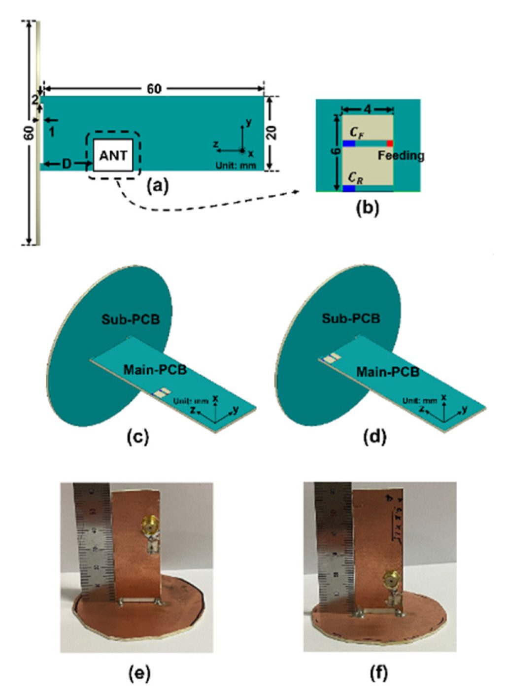
(a) Geometry of the overall structure, (b) GradiAnt configuration, (c) GradiAnt Position 1 (D = 29 mm), (d) Gradi-Ant Position 2 (D = 0.5 mm), (e) fabricated GradiAnt Position 1, and (f) fabricated GradiAnt Position 2.
It is well known that the GradiAnt’s performance depends on the coupling between the resonant loop of the GradiAnt and the PCB ground. According to the reaction theorem, the coupling between the GradiAnt and the PCB ground can be expressed as follows:
where H̄PCB denotes the magnetic field formed by the currents on the PCB ground, and M̄GradiAnt represents the equivalent magnetic current of the loop electric current fed by the source. The operation of the GradiAnt is that the energy of the M̄GradiAnt is coupled and transferred to the current mode of the electrically large PCB ground, and the coupled energy of the current mode is efficiently radiated into the free space. Therefore, the GradiAnt needs to be designed at a location with strong current distribution, and a strong H̄PCB is formed on the PCB ground.
As shown in Fig. 1, if the sub-PCB is sufficiently larger than the main PCB, the electrical length of the main PCB in the z direction looks approximately double, based on the image theory, and the strong H̄PCB of the overall complex PCB is formed near the sub-PCB [6]. The magnitude of the current distribution is reduced by moving far away from the sub-PCB. Therefore, designing the GradiAnt closer to the sub-PCB results in the maximum coupling between the complex PCB and the Gradi-Ant, and better GradiAnt performance is anticipated [7].
The GradiAnt performance improvement can be understood through the equivalent magnetic current model. When the electric current flows through the loop-type antenna, magnetic fields are generated perpendicular to the plane of the loop-type circuit, and the equivalent magnetic current is considered H̄ = jwμH̄. Fig. 2(a) and 2(b) show the induced magnetic current on the sub-PCB of GradiAnt Position 1 and GradiAnt Position 2, respectively. In Fig. 2, the magnetic current formed by the Gradi-Ant flows in the x direction, tangential to the surface of the sub-PCB. Based on the image theory, when the GradiAnt is located near the sub-PCB, the magnetic current formed by the GradiAnt creates an induced magnetic current on the surface of the sub-PCB. The induced magnetic current on the sub-PCB has the same direction as the magnetic current formed by the GradiAnt, enhancing the total radiation performance. Therefore, GradiAnt Position 2 has better coupling with the complex PCB structure and improved performance. In other words, if the sub-PCB is sufficiently larger than the main PCB, the total magnetic current formed by the overall antenna structure has nearly twice the magnitude, and the GradiAnt’s improved performance is expected.
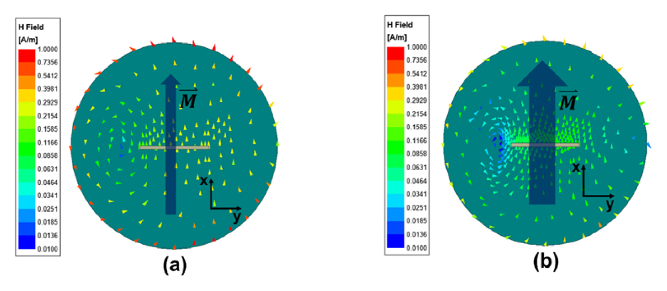
Induced magnetic current on the sub-PCB of (a) GradiAnt Position 1 and (b) GradiAnt Position 2.
III. Simulation and Measurement Results
The GradiAnts were simulated using the Ansoft High-Frequency Structure Simulation (HFSS), and the fabricated GradiAnts were measured by the Keysight E5071C network analyzer. Fig. 3 shows the reflection coefficients (S11) according to the GradiAnt positions. The simulated 3:1 VSWR (voltage standing wave ratio) bandwidth of GradiAnt Position 1 was 80 MHz, and that of GradiAnt Position 2 was over two times greater at 180 MHz. The measured reflection coefficient results were also similar to the simulated results. The measured 3:1 VSWR bandwidths of GradiAnt Position 1 and GradiAnt Position 2 were 105 MHz and 235 MHz, respectively. As a result of moving the GradiAnt position from the center of the main PCB to near the sub-PCB, the impedance bandwidth was increased. Accordingly, when the GradiAnt was designed to be near the sub-PCB, the GradiAnt’s performance was improved because of the increased coupling between the antenna and the complex PCB.
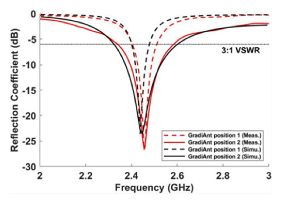
Simulated and measurement S11 of GradiAnt in different positions.
The radiation performance of the fabricated antennas was measured in a 6 m × 3 m × 3 m 3D Cellular Telecommunication Industry Association (CTIA) Over-The-Air (OTA) chamber. The measured total efficiencies according to the GradiAnt positions are shown in Fig. 4. Total efficiency includes reflection mismatch efficiency and radiation efficiency. GradiAnt Position 1 showed 50%–60% efficiency at 2.38–2.48 GHz (frequency band), whereas GradiAnt position 2 had 50%–70% efficiency at 2.22–2.6 GHz. The efficiency bandwidth of GradiAnt Position 2 with more than 50% efficiency was significantly wider than that of GradiAnt Position 1.
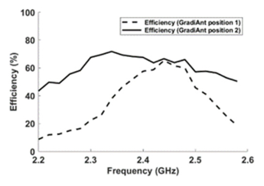
Total efficiency measured according to the GradiAnt position.
Fig. 5 shows the measured radiation patterns according to the GradiAnt position at 2.45 GHz. GradiAnt Position 1 and Gradi-Ant Position 2 generated omnidirectional radiation patterns on the xy plane. These results indicate that the two GradiAnt on the complex PCB are designed to function as dipole-type radiators along the z direction because of the magnetic coupling from the looptype current. Although the GradiAnt is designed close to the vertically arranged PCB, the omnidirectional property does not change. Alternatively, there is a slight difference in the radiation patterns of the yz and xz planes, depending on the position of the GradiAnt, which is considered to be caused by the sub-PCB radiation.
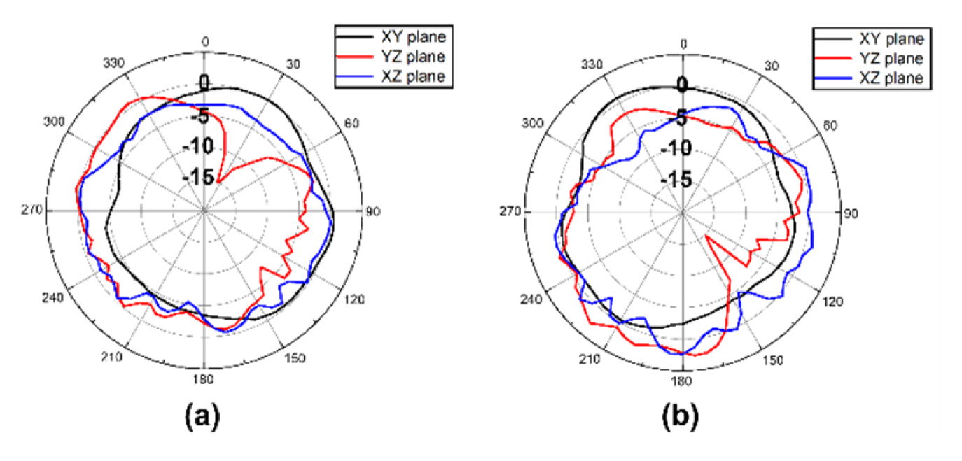
Measured radiation patterns of (a) GradiAnt Position 1 and (b) GradiAnt Position 2.
IV. Conclusion
In this paper, we have presented our study on the GradiAnt’s performance according to different positions in a complex PCB with two vertically arranged grounds. Because of the vertically arranged sub-PCB, the current distribution of the main PCB was maximum near the sub-PCB, and the impedance bandwidth and the efficiency bandwidth were improved by designing the GradiAnt close to the sub-PCB. The omnidirectional property when the GradiAnt was designed to be in the center of the main PCB was maintained even when it was re-positioned near (OR moved close to) the sub-PCB. These GradiAnt performance improvements were verified by the simulation and measurement results. This idea can be applied to other ground shapes and different frequency bands.
Acknowledgments
This study was supported by the National Research Foundation of Korea through a grant from the Korean government (Ministry of Science and ICT) (No. 2019 R1F1A1063993).