


I. Introduction
II. Proposed Equivalent Circuit Model for Double Exponential Pulse Generator
1. Double Exponential Pulse as Conducted Disturbance Noise Source
KDE: Modifying factor;
Î: Maximum peak current;
╬▒, ╬▓: The characteristic parameters;
tr: The interval of the time required for the leading edge of a pulse to rise from 10% to 90% of the peak pulse amplitude;
tFWHM: The time interval from 0.5Î to half of the maximum peak current Î;
tpeak: The time at the maximum peak current Î.
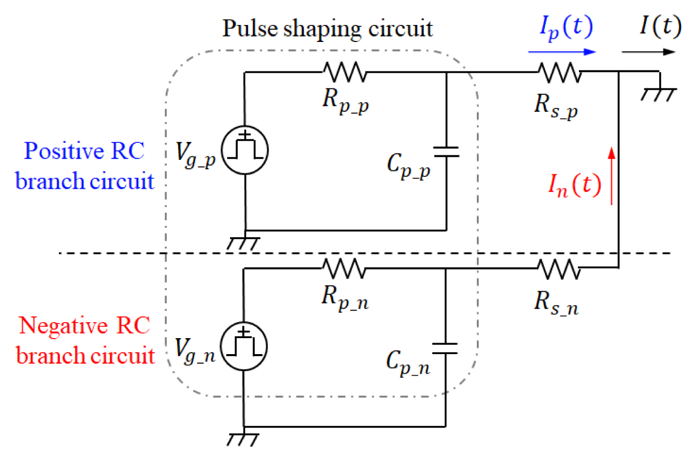
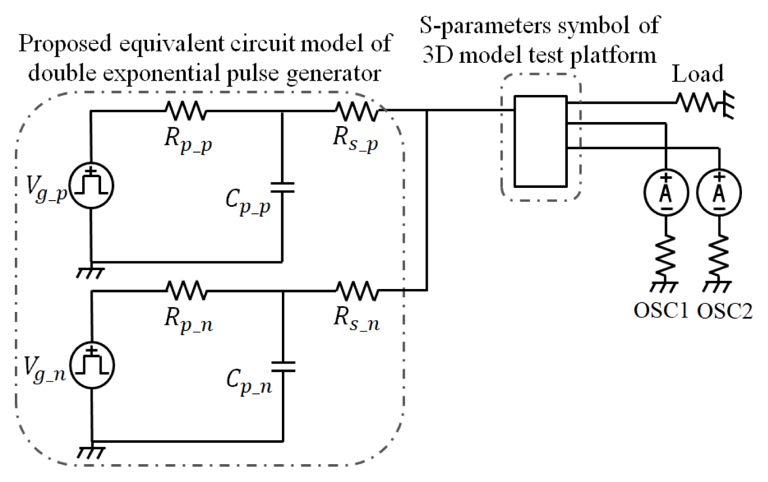
2. Proposed Equivalent Circuit Model
Rs: Source impedance resistance;
Rp, Cp: Pulse shaping circuit resistance, capacitor;
Vg: Magnitude of the step pulse generator;
Pulse shaping circuit: Part of the equivalent circuit to determine the time constant and sign of the step pulse;
Underscore p, n: Circuit components belonging to a positive or negative RC branch circuit.
3. Double Exponential Pulse Modeling
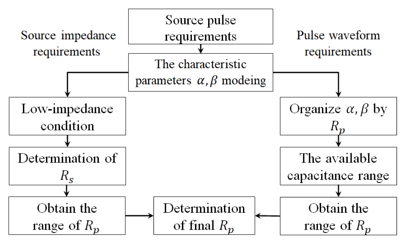
III. Proposed Design Methodology for Equivalent Circuit Model
1. Characteristic Parameter ╬▒,╬▓ Modeling
2. Proposed Equivalent Circuit Model Design Methodology
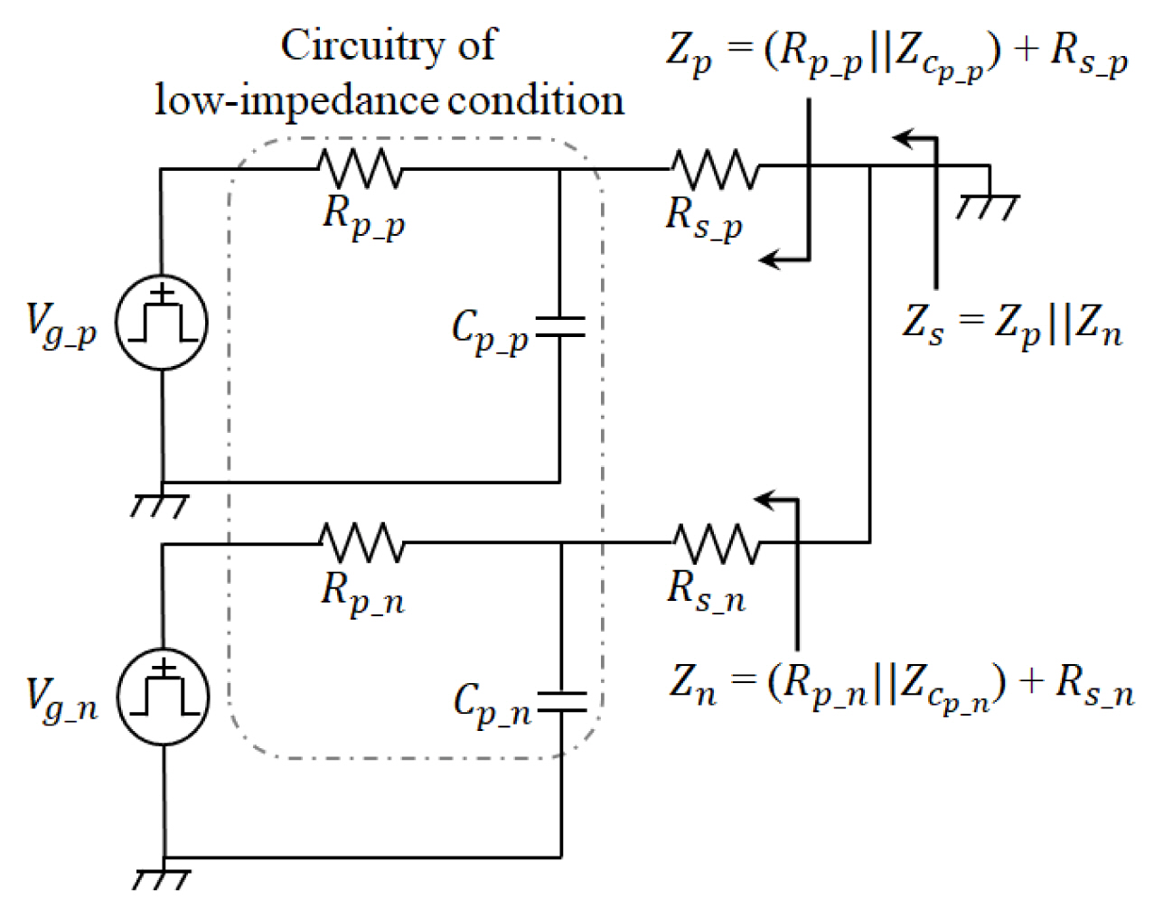
1) Source impedance requirement design
2) Pulse waveform requirement design
3) Proposed equivalent circuit model design
3. Design Example
Step 1 (The characteristic parameters ╬▒,╬▓ modeling): The source pulse requirements of the CEP1 test mode and modeled characteristic parameters, ╬▒,╬▓, derived from Eqs. (7)ŌĆō(8) are listed in Table 3. The frequency range applied in the design example is 100 kHzŌĆō200 MHz, which is the common HEMP environment frequency range.
Step 2 (Source impedance requirement design): The low-impedance condition is applied, and Rs is determined to be 800 ╬® using Eqs. (13)ŌĆō(14). With the modeled characteristic parameters and the value of Rs, the maximum range of Rp_n is determined to be 30 ╬® using Eq. (19), where Kn = 30. In the case of the CEP1 test mode, Bp is larger than one, and the range of Rp_p can be set equal to the range of Rp_n to satisfy the low-impedance condition.
Step 3 (Pulse waveform requirement design): The available capacitance ranges are set to Cp_min = 1 pF, Cp_max = 1 mF. The range of Cp for positive Rp can be calculated using Eq. (20) along with the circuit components in Step 1. The combined capacitance range is determined as 0.13 nF < Cp_p < 1 mF and 1pF < Cp_n < 1 mF. With the determined capacitance range, 0.1 m╬® < Rp_p < 0.5 M╬® and 6.1 ╬╝╬® < Rp_n < 0.23 ╬®, is obtained from Eq. (19).
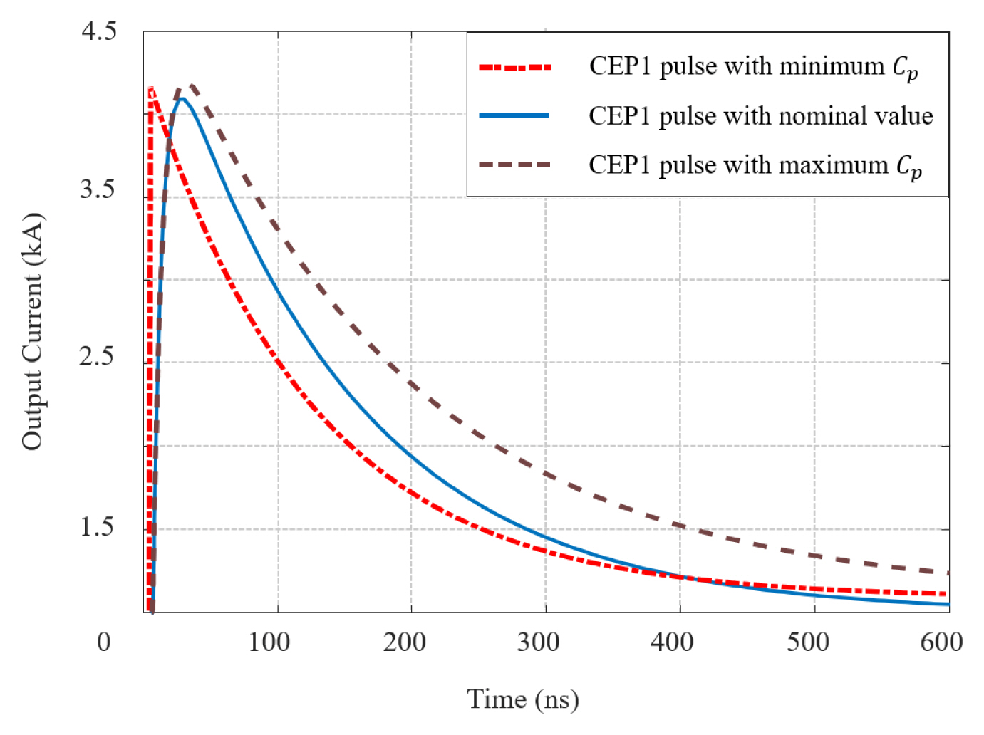
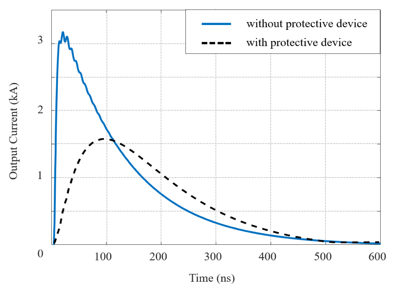
Step 4 (Proposed equivalent circuit model design): The design parameters determined in Step 1 to Step 3 are summarized in Table 4. Circuit simulation is performed with the determined circuit components. In Fig. 5, the pulse waveform characteristics of the generated double exponential pulses vary according to the ranges of Cp obtained using the proposed design methodology. The resistance values, Rp_p and Rp_n, were chosen to be 20 Ohms and 0.2 Ohms, respectively, as nominal values within the range derived in Step 3. Table 5 presents a comparison of the parameters of the source pulse requirements and the circuit simulation results. As presented in Fig. 5 and Table 5, with the proposed equivalent circuit model and design methodology, it is confirmed that it is possible to design a double exponential pulse satisfying the standard error of the source pulse requirements.