J. Electromagn. Eng. Sci Search

CLOSE


J. Electromagn. Eng. Sci > Volume 23(3); 2023 > Article
Jang, Jung, Lee, Cho, Park, Lim, Kim, Park, and Yoon: LTCC-Based DC-DC Converter for Reduction of Switching Noise and Radiated Emissions

Abstract

In this study, a low-temperature co-fired ceramic (LTCC)-based direct current (DC)-DC converter is proposed for reducing stray inductance and mitigating electromagnetic interference. The dominant radiating loop of the proposed LTCC-based DC-DC converter features a multilayer design, which helps suppress noise sources and reduce radiated emissions. The peak voltage of switching noise for the proposed DC-DC converter at the frequency of 500 kHz is approximately 8.98% lower than that of a conventional DC-DC converter. In addition, the radiated emission level of the proposed DC-DC converter is lower than that of the conventional DC-DC converter. In sum, the proposed LTCC-technology-based multilayer design reduces the peak voltage of switching noise and the radiated emission of the DC-DC converter.

I. Introduction

With the advent of portable devices, such as tablets, smartphones, and laptops, lightweight electronic devices with a small volume are in high demand [13]. Additionally, the demand for flat and thin electronic devices such as laptops and televisions has been growing [46]. To small-volume, light-weight, and flat electronic devices, researchers have focused on developing a suitable power-conversion system [79]. Wide bandgap (WBG) semiconductors, such as gallium nitride (GaN) and silicon carbide (SiC), can be used in such power conversion systems. WBG-semiconductor-based power devices can operate at high frequencies. Moreover, owing to their fast-switching frequency, passive components can be designed to be compact and lightweight. Therefore, lightweight and small power conversion systems are possible [1013]. However, as the switching frequency of a power conversion system increases, issues related to electromagnetic interference (EMI) can emerge. Therefore, various studies have been conducted to reduce EMI by curbing stray inductances in power conversion systems [1416].
Low-temperature co-fired ceramic (LTCC) is generally used in wireless applications owing to its excellent performance at high frequencies [1719]. Compared to the cheap flame retardant 4 (FR-4) substrate, LTCC offers superior thermal conductivity and heat dissipation. The thermal conductivities of FR-4 and LTCC are 0.2–0.4 and 4–5 W/m·K, respectively [20]. In addition, LTCC has a high wiring density with vias that are filled with silver paste, and it benefits from multilayer circuits that reduce stray inductance [21].
With this background, in this study, an LTCC-based direct current (DC)-DC converter is proposed to reduce stray inductance and radiated emissions for achieving electromagnetic compatibility (EMC). Two types of LTCC-based DC-DC converters are designed and built for comparison: one is based on a conventional design, wherein the ground and power planes are in separate layers. In the other design, the ground and power planes exist in each layer, which is observed to be effective for reducing the stray inductance of the dominant radiating loop, which reduces the peak voltage of switching noise and the radiated emission level.
The remainder of this paper is organized as follows: in Section II, the designs of the circuit and LTCC boards of the DC-DC converter are introduced, along with the simulated characteristics of the LTCC board. Section III presents the measured power-conversion and radiated-emission characteristics of the DC-DC converters compared herein. The suitability of LTCC as a substrate for DC-DC converters to achieve EMC and efficient power conversion is demonstrated. In Section IV, we introduce the proposed DC-DC converter based on LTCC technology and discuss the superiority of LTCC as a substrate. Finally, in Section V, we present the conclusions of this study.

II. Design of DC-DC Converter and LTCC Substrate

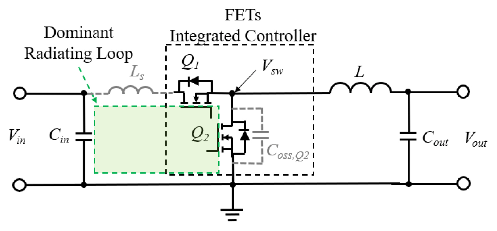
Fig. 1 shows the designed buck converter circuit as one of the DC-DC converters. Herein, the buck converter was designed with an input voltage (Vin) of 12 V, output voltage (Vout) of 5 V, output power of 35 W, and switching frequency of 500 kHz. The converter comprises an input capacitor (Cin), an output capacitor (Cout), a power inductor (L), and a field-effect transistor (FET)-based integrated controller. Owing to alternate switching of the two FETs (Q1, Q2), noise can be generated at the voltage of switching node (Vsw) of the buck converter. Typically, noise is generated at the switching node through two mechanisms: body-diode reverse recovery and FET switching [2224]. The reverse-recovery noise of the buck converters is determined by the characteristics of the body diode in the FETs, whereas the switching noise is generated by the stray inductance (Ls) of the dominant radiating loop and the output capacitance of Q2 (Coss,Q2). The frequency of switching-noise (fnoise) and the peak voltage of switching noise (Vsw,peak) are defined as follows [25, 26]:
(1)
fnoise=12πLs·Coss,Q2,
(2)
Vsw,peak=Lsdidt+Vin,
where didt is the rate of current change. Because the stray inductance is proportional to the peak voltage of switching noise and the generated noise can be radiated through the dominant radiating loop, the stray inductance of the dominant radiating loop should be minimized for EMI.
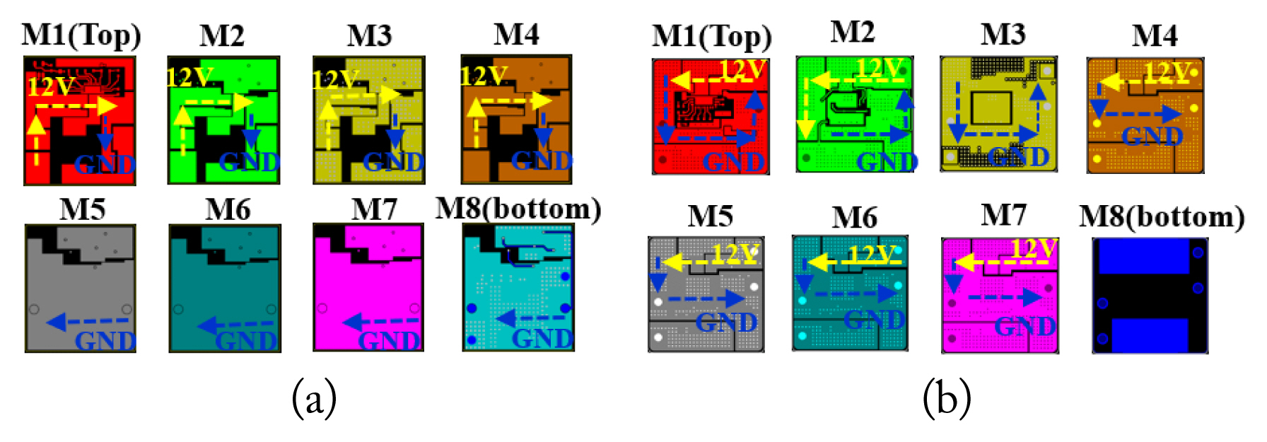
For comparison, Fig. 2 depicts each layer of the designed substrates for the buck converter. The substrates were composed of eight metal layers M1–M8. The yellow and blue arrows indicate the directions of the noise currents flowing to the power and ground planes, respectively.
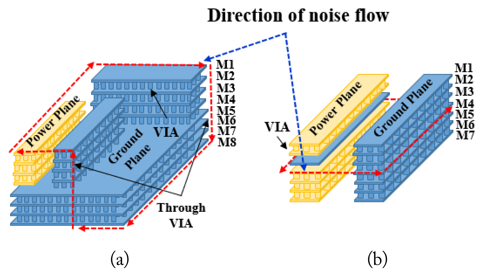
Fig. 3 shows the noise currents flowing through the dominant radiating loops of the designed substrates when all layers are stacked. The metals constituting each layer were electrically connected through vias based on the plane classification. As illustrated in Fig. 3(a), in the conventional design, the ground and power planes were separated vertically whereby the generated noise flowed vertically through the via that connected each of the layers. Moreover, the proposed substrate was designed to reduce the stray inductance of the dominant radiating loop by placing the ground and power planes parallel to each other in each layer, except in layers M3 and M8, to ensure electrical connection of other components, as illustrated in Fig. 3(b).
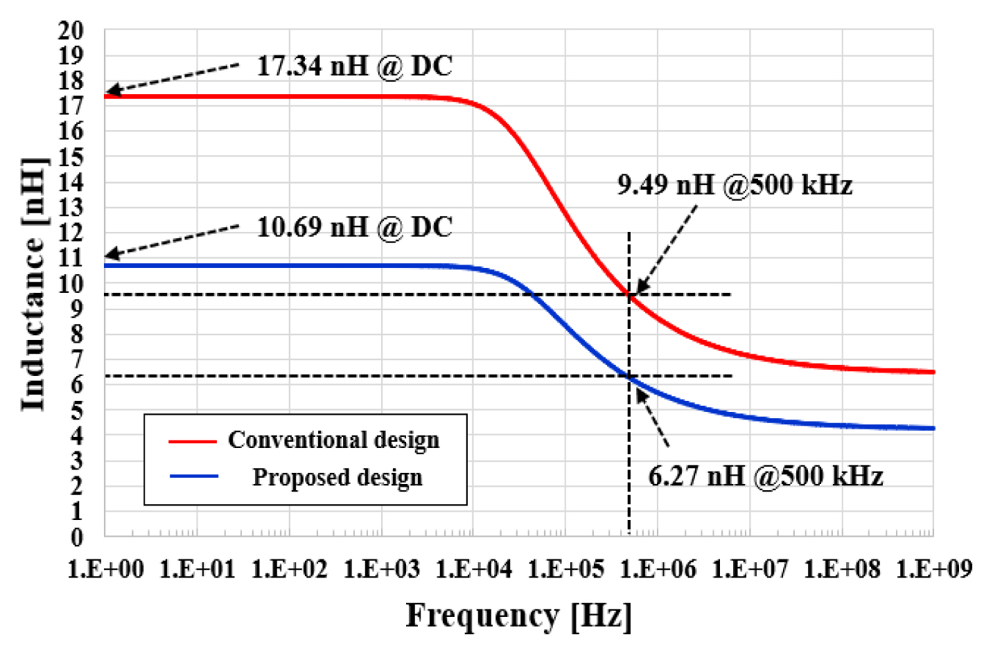
Fig. 4 shows the simulated frequency-dependent stray inductance of the dominant radiating loop. We used the Ansys Q3D tool to simulate the stray inductance. The stray inductances of the conventional and proposed designs were 17.34 and 10.69 nH at DC, respectively. In addition, the stray inductances of the conventional and proposed designs were 9.49 and 6.27 nH, respectively, at 500 kHz, which was the switching frequency of the designed buck converter. The simulation results confirmed that the stray inductance of the proposed design was lower than that of the conventional design.
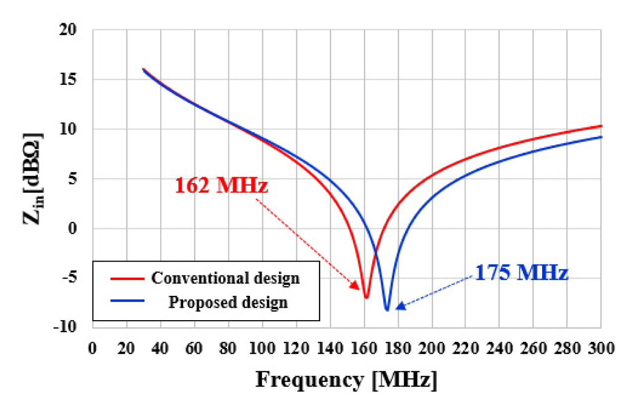
Because the generated noise can be radiated owing to the antenna efficiency of the substrate [27], the antenna characteristics of the dominant radiating loop were simulated at various frequencies. We used Ansys HFSS simulation software to simulate the radiation properties. In a previous analysis of the switching noise of the buck converter, the output capacitance of the FET used in the integrated circuit, calculated using Eq. (1), was approximately 100 pF. Therefore, a 100 pF capacitance was selected for simulating the radiation properties. Fig. 5 depicts the frequency-dependent input impedances (Zin) of the dominant radiating loops of the conventional and proposed buck converter designs. The simulated resonant frequencies of the conventional and proposed buck converter designs were 162 and 175 MHz, respectively [25].
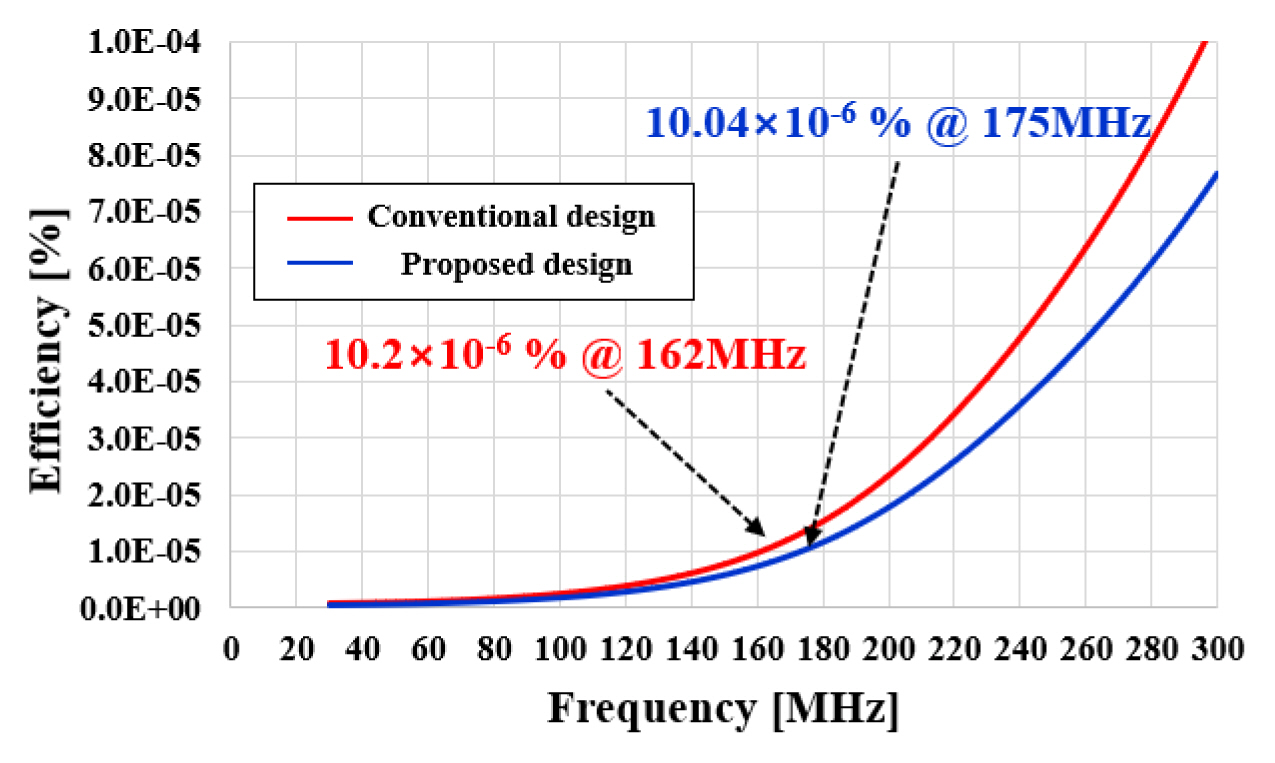
Fig. 6 illustrates the frequency-dependent radiation efficiencies of the dominant radiating loops of the conventional and proposed buck converters. The simulated radiation efficiencies of the conventional and proposed buck converters were 10.2 × 10⁻⁶% at 162 MHz and 10.04 × 10⁻⁶% at 175 MHz, respectively. The radiation efficiencies of the proposed and conventional buck converters were similar at the resonant frequency. However, the simulation results confirmed that the frequency-dependent radiation efficiency of the proposed buck converter was lower than that of the conventional buck converter.

III. Measured Results

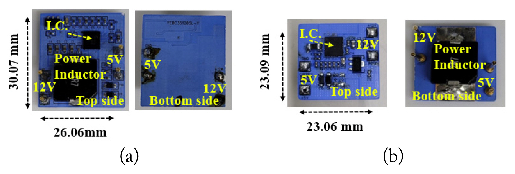
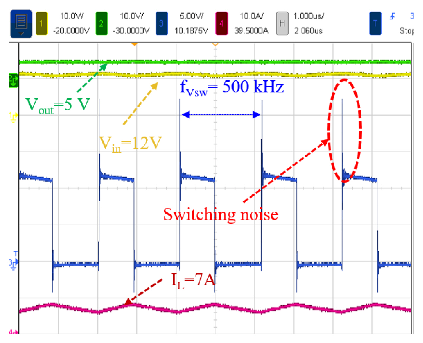
Fig. 7 shows the built buck converters. The width and length of the conventional buck converter were 26.06 and 30.07 mm, respectively, whereas those of the proposed buck converter were 23.06 mm and 23.09 mm. Fig. 8 shows the operating characteristics of the conventional buck converter for the output power of 35 W. The buck converter operated as designed. In addition, switching noise was generated at Vsw. The conventional and proposed buck converters were compared to verify the switching noise characteristics.
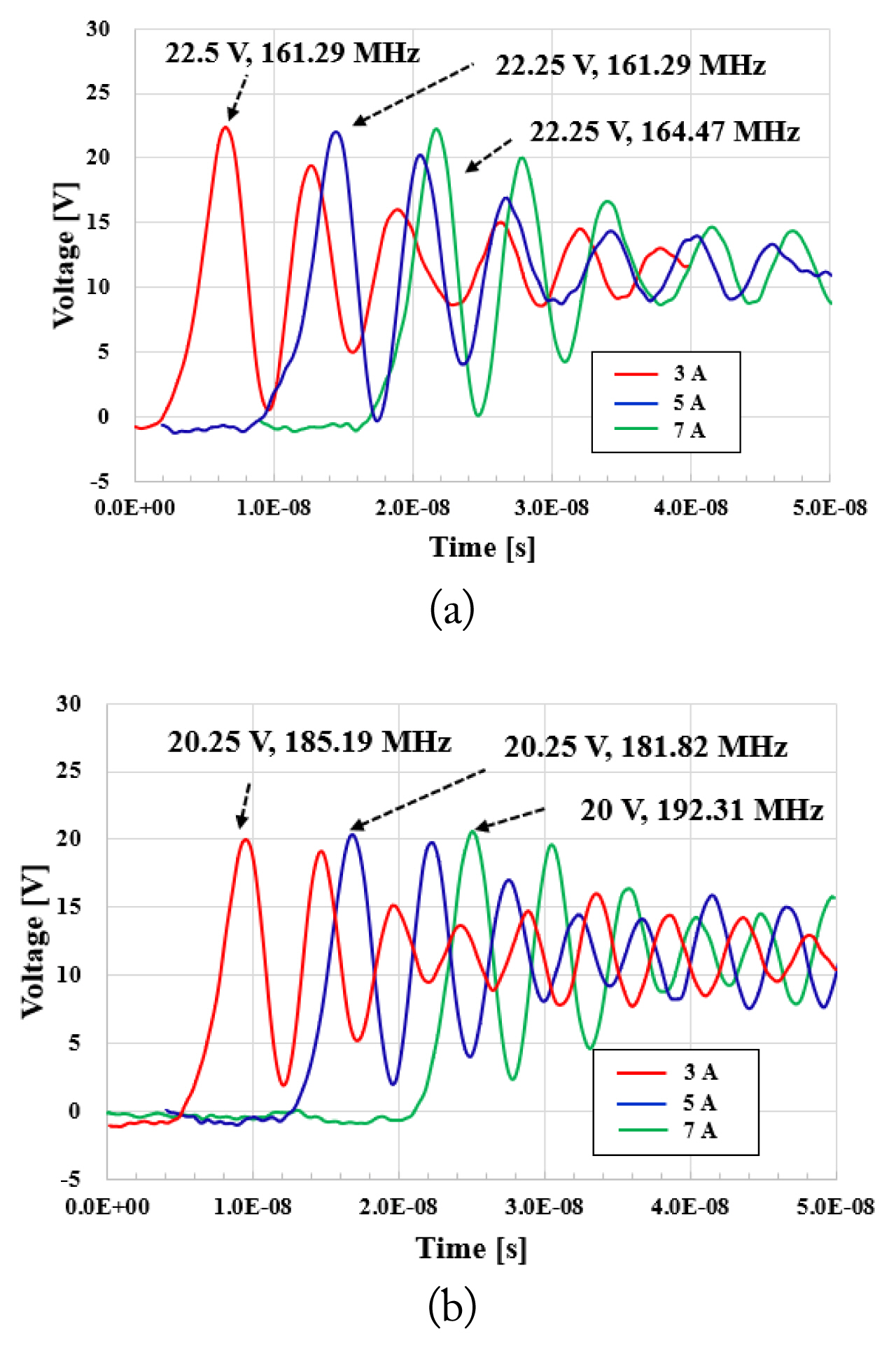
The resonant frequency and peak voltage of switching noise of the built converters were measured, as illustrated in Fig. 9. The peak voltages corresponding to the switching noise of the conventional and proposed buck converters were 22.5 and 20.25 V at the output current of 3 A, 22.25 and 20.25 V at the output current of 5 A, and 22.25 and 20 V at the output current of 7 A, respectively. In addition, the switching noise frequencies of the conventional and proposed buck converters were 161.29 and 185.19 MHz at the output current of 3 A, 161.29 and 181.82 MHz at the output current of 5 A, and 164.47 and 192.31 MHz at the output current of 7 A, respectively. These results confirmed that the stray inductance of the proposed buck converter was lower than that of the conventional buck converter.
The measured operating characteristics of the two buck converters are summarized in Table 1. The proposed design had a lower peak voltage of switching noise (Vsw,peak) than that of the conventional design owing to its lower stray inductance. The output capacitance (Coss,Q2) was calculated using Eq. (1) and the measured switching noise frequency and simulated stray inductance. The calculated output capacitance value was approximately 100 pF. Furthermore, the resonant frequencies of the conventional and proposed buck converters were similar to the corresponding simulated values.
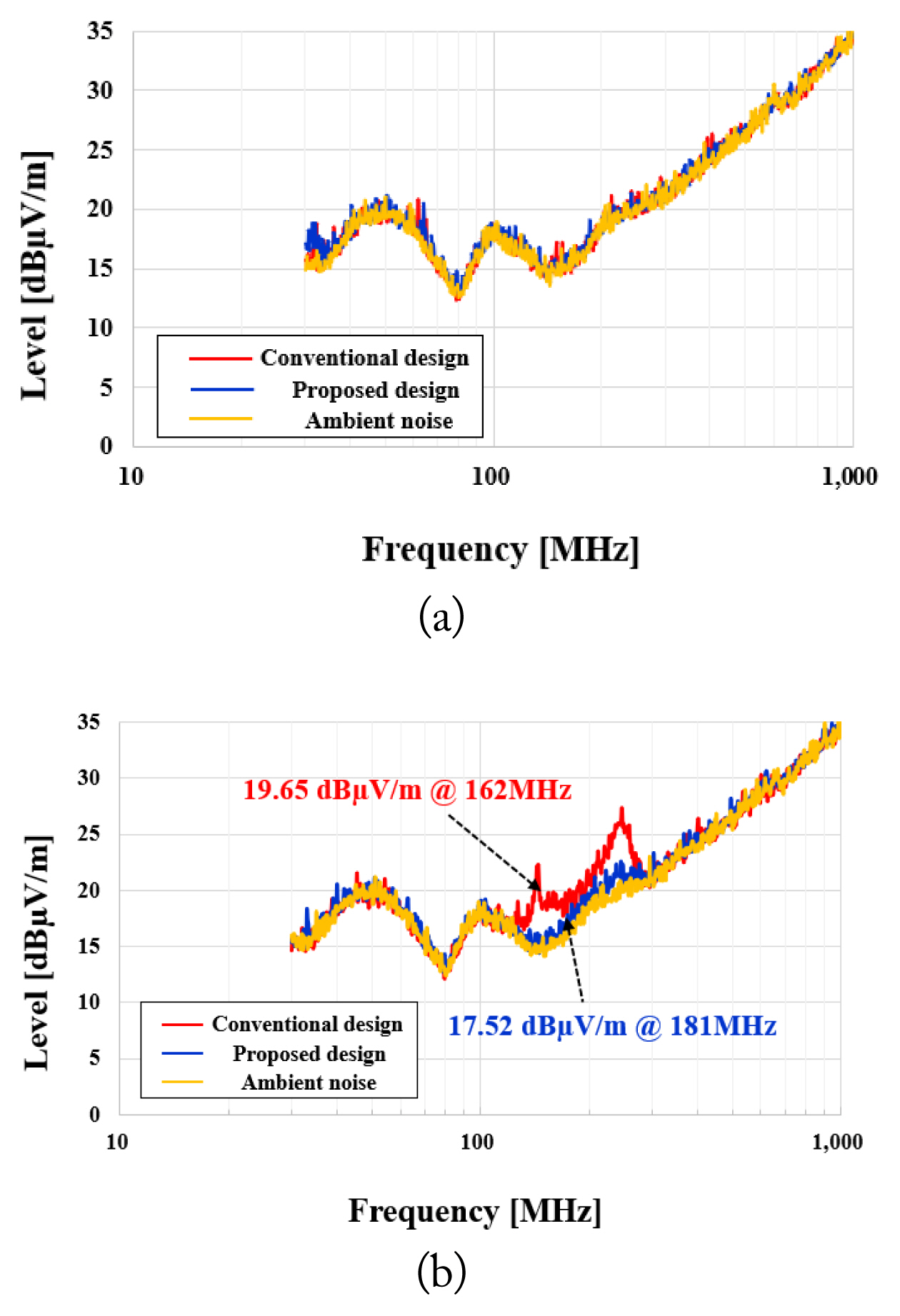
Fig. 10 depicts the measured radiated emission levels of the buck converters. To minimize the effect of the noise generated by electronic devices, such as the electrical load and power supply, a 12 V battery and a discrete resistor were used. Considering the difficulty of configuring the resistance at the output current of 3 A or 7 A, the accumulated peak radiated emission levels of the buck converters were determined at the output current of 5 A. The radiated emission levels of the buck converters were measured in accordance with the CISPR 16-1-1 and IEC 61000-6-3 standards. The distance between the turntable on which the buck converter was loaded and the receiver antenna was 10 m. In addition, the radiated emission level of the buck converter was determined by moving the receiver antenna over distances of 1–4 m in the horizontal and vertical directions [28]. When the antenna was moved in the vertical direction, noise from the buck converter could not be detected because of the ambient noise level, as illustrated in Fig. 10(a).
However, when the antenna was moved in the horizontal direction, the noise emitted by the buck converters was detected, as illustrated in Fig. 10(b). The radiated emission level of the proposed buck converter (17.52 dBμV/m at 181 MHz) was lower than that of the conventional buck converter (19.65 dBμV/m at 162 MHz) by approximately 2 dBμV/m lower at the resonant frequency. Although the radiation efficiencies of both buck converters were similar at the resonant frequency, the radiated emission level of the proposed buck converter was lower than that of the conventional buck converter at the resonant frequency. This was because the generated noise level was lower owing to lower stray inductance in the proposed design.
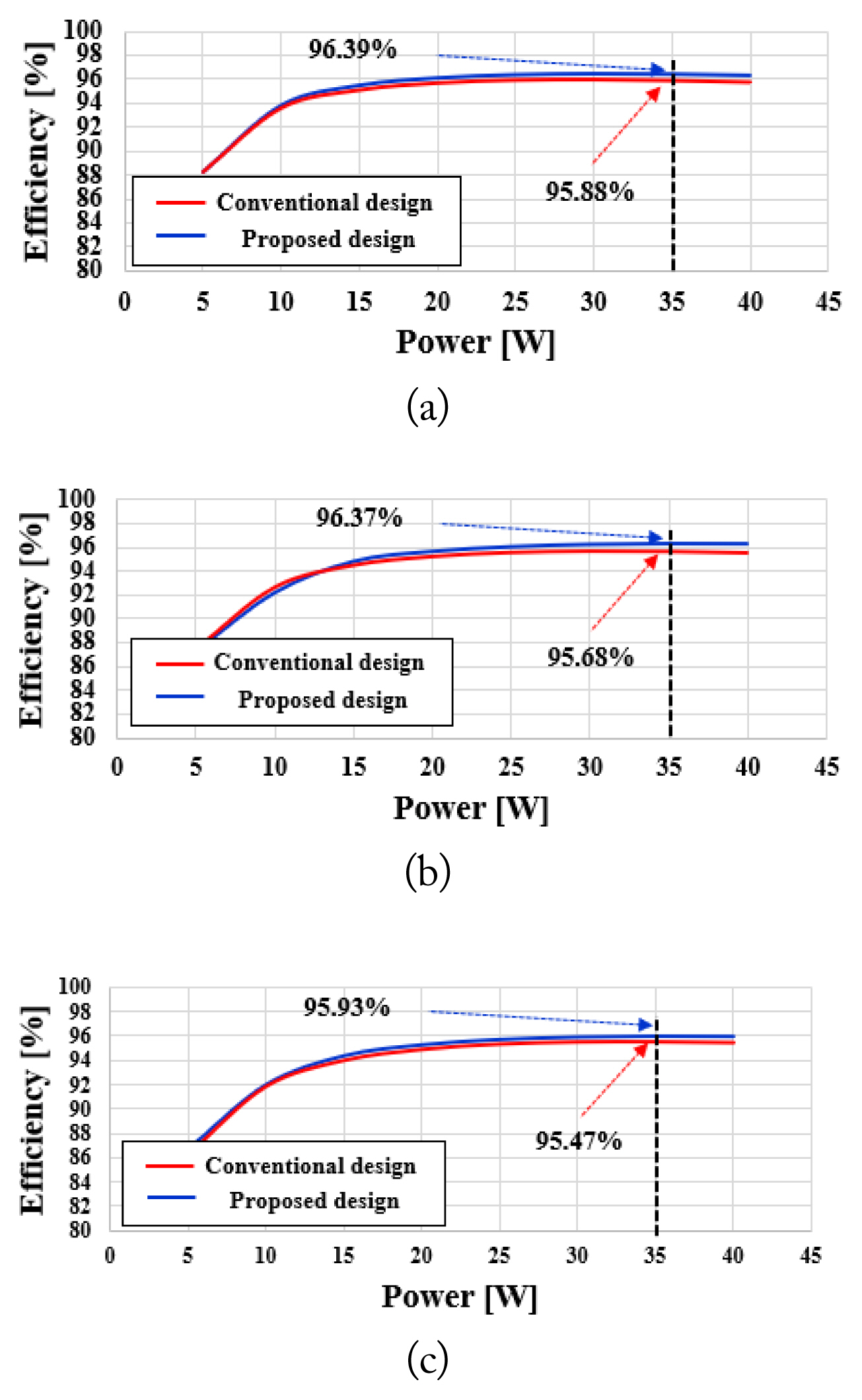
Fig. 11 depicts the power conversion efficiencies, which represent a major characteristic of power conversion systems, of the built buck converters. The measured power conversion efficiencies of the conventional and proposed buck converters were 95.88% and 96.39% at the input voltage of 10.8 V, 95.68% and 96.37% at the input voltage of 12 V, and 95.47% and 96.93% at the input voltage of 13.2 V, respectively; the output power was 35 W in all cases.

IV. Discussion

Table 2 shows a performance comparison of the LTCC-based DC-DC converters built herein. In the pursuit of a small volume, a low-profile LTCC inductor has been reported as a substrate in the literature [29, 30]. This low-profile LTCC inductor can be designed to have a high switching frequency. However, as the switching frequency increases, the efficiencies of the DC-DC converter with the low-profile LTCC inductor decrease to less than 90%. In addition, to achieve high power conversion efficiency, a DC-DC converter with an LTCC substrate was reported. Owing to the low power consumption, high wiring density, and high thermal conductivity of LTCC, high-power conversion efficiencies exceeding 90% were achieved with this DC-DC converter [20, 21]. As reported in [21], the required radiated emission level characteristics were realized.
The LTCC-based DC-DC converter design proposed herein reduced the switching noise and radiated emission level without adversely affecting the power conversion efficiency. To further reduce noise, snubber or gate circuits, which consist of passive components, could be used. Although these solutions may reduce the noise, the power loss due to their passive components can degrade the power conversion efficiency. Note that the efficiency of the proposed LTCC-based DC-DC converter does not decrease, unlike those of the conventional designs.

V. Conclusion

In this study, we presented an LTCC-based DC-DC buck converter that reduced the switching noise and radiated emission level, thereby facilitating the realization of EMC. By utilizing a multilayer design based on LTCC technology, the switching noise and radiated emission level of the DC-DC converter were reduced. Notably, the power conversion efficiency, which is one of the significant characteristics of power conversion systems, was retained unchanged. Therefore, the LTCC substrate is expected to be used in power conversion systems with high switching speed, high efficiency, and low EMI.

Acknowledgments

This work was supported by the National Research Council of Science & Technology (NST) grant by the Korea government (MSIT) (No. CRC-19-02-ETRI), the Institute for Information & Communications Technology Planning & Evaluation (IITP) grant by the Korea government (MSIT) (No. 2018-0-01138), and the Institute of Information & communications Technology Planning & Evaluation (IITP) grant funded by the Korea government (MSIT) (No. 2020-0-00839, Development of Advanced Power and Signal EMC Technologies for Hyper-connected E-Vehicles).

Fig. 1
Simplified circuit of designed buck converter.
jees-2023-3-r-165f1.jpg
Fig. 2
Layers of designed substrate: (a) conventional design and (b) proposed design.
jees-2023-3-r-165f2.jpg
Fig. 3
Dominant radiating loop of designed substrates: (a) conventional design and (b) proposed design.
jees-2023-3-r-165f3.jpg
Fig. 4
Simulation results showing stray inductance of the dominant radiating loop.
jees-2023-3-r-165f4.jpg
Fig. 5
Simulation results showing input impedance of the dominant radiating loop.
jees-2023-3-r-165f5.jpg
Fig. 6
Simulation results showing radiation efficiency of the dominant radiating loop.
jees-2023-3-r-165f6.jpg
Fig. 7
Built buck converters: (a) conventional design and (b) proposed design.
jees-2023-3-r-165f7.jpg
Fig. 8
Operating characteristics of the conventional buck converter.
jees-2023-3-r-165f8.jpg
Fig. 9
Measured switching noise: (a) conventional design and (b) proposed design.
jees-2023-3-r-165f9.jpg
Fig. 10
Measured radiated emission levels of the conventional and proposed buck converters: (a) vertical and (b) horizontal.
jees-2023-3-r-165f10.jpg
Fig. 11
Power conversion efficiencies of built buck converters: (a) Vin = 10.8 V, (b) Vin = 12 V, and (c) Vin = 13.2 V.
jees-2023-3-r-165f11.jpg
Table 1
Summary of measurements
Conventional design Proposed design
Output current (A) 3 5 7 3 5 7
Peak voltage of switching noise (V) 22.5 22.25 22.25 20.25 20.25 20
Stray inductance (nH) 9.49 9.49 9.49 6.27 6.27 6.27
Frequency of switching noise (MHz) 161.29 161.29 164.47 185.19 181.82 192.31
Output capacitance (pF) 102 102 98.7 117 122 109
Table 2
Comparison of several LTCC-based DC-DC converters
Study Type of input (V) Output (V/A) Switching frequency (kHz) Efficiency (%) Note
Lim et al. [29] 5 1.1 / 16 1300 <85 -
Su et al. [30] 12 1.2 / 15 1000, 2000, 3000 88, 85, 82 -
Jung et al. [20] 48 12 / 8.3 200 95.5 -
Jung et al. [21] 48, 36 5 / 3.1, 12 / 2 150, 600 92.9, 93.6 Radiated emission test
This work 12 5 / 7 500 96.2 Radiated emission test

References

1. S. A. Hasib, S. Islam, R. K. Chakrabortty, M. J. Ryan, D. K. Saha, M. D. Ahamed, and et al, "A comprehensive review of available battery dataset, RUL prediction approaches, and advanced battery management," IEEE Access, vol. 9, pp. 86166–86193, 2021.
crossref
2. D. Hou, F. C. Lee, and Q. Li, "Very high frequency integrated voltage regulator for small portable devices," In: Proceedings of the 2016 IEEE Energy Conversion Congress and Exposition (ECCE); Milwaukee, WI. 2016, pp 1–7.
crossref
3. J. Seo, I. Yoon, J. Jung, J. Ryoo, J. Park, W. Lee, D. Ko, and J. Oh, "Miniaturized dual-band broadside/endfire Antennain-Package for 5G smartphone," IEEE Transactions on Antennas and Propagation, vol. 69, no. 12, pp. 8100–8114, 2021.
crossref
4. P. Sun, J. Park, J. H. Kwon, and S. M. Hwang, "Development of slim speaker for use in flat TVs," IEEE Transactions on Magnetics, vol. 48, no. 11, pp. 4148–4151, 2012.
crossref
5. Y. Xiao, S. Advani, D. Shin, N. Chang, J. J. Sampson, and V. Narayanan, "A saliency-driven LCD power management system," IEEE Transactions on Very Large Scale Integration (VLSI) Systems, vol. 24, no. 8, pp. 2689–2702, 2016.
crossref
6. K. L. Wong, L. C. Chou, and C. M. Su, "Dual-band flat-plate antenna with a shorted parasitic element for laptop applications," IEEE Transactions on Antennas and Propagation, vol. 53, no. 1, pp. 539–544, 2005.
crossref
7. S. Du, B. Wu, D. Xu, and N. R. Zargari, "A transformerless bipolar multistring DC–DC converter based on series-connected modules," IEEE Transactions on Power Electronics, vol. 32, no. 2, pp. 1006–1017, 2017.
crossref
8. M. A. Bakar, M. F. Alam, and K. Bertilsson, "Modeling and characterization of series connected hybrid transformers for low-profile power converters," IEEE Access, vol. 8, pp. 53293–53306, 2020.
crossref
9. S. Gao and H. Wang, "A new approach integrated magnetics double-frequency DC/DC converter," IEEE Access, vol. 8, pp. 148301–148314, 2020.
crossref
10. H. Moradisizkoohi, N. Elsayad, and O. A. Mohammed, "Experimental demonstration of a modular, quasi-resonant bidirectional DC–DC converter using GaN switches for electric vehicles," IEEE Transactions on Industry Applications, vol. 55, no. 6, pp. 7787–7803, 2019.
crossref pdf
11. A. Jafari, M. S. Nikoo, N. Perera, H. K. Yildirim, F. Karakaya, R. Soleimanzadeh, and E. Matioli, "Comparison of wide-band-gap technologies for soft-switching losses at high frequencies," IEEE Transactions on Power Electronics, vol. 35, no. 12, pp. 12595–12600, 2020.
crossref
12. J. Xu, L. Gu, Z. Ye, S. Kargarrazi, and J. M. Rivas-Davila, "Cascode GaN/SiC: a wide-bandgap heterogenous power device for high-frequency applications," IEEE Transactions on Power Electronics, vol. 35, no. 6, pp. 6340–6349, 2020.
crossref
13. R. Sun, J. Lai, W. Chen, and B. Zhang, "GaN power integration for high frequency and high efficiency power applications: a review," IEEE Access, vol. 8, pp. 15529–15542, 2020.
crossref
14. Y. Xie, C. Chen, Z. Huang, T. Liu, Y. Kang, and F. Luo, "High frequency conducted EMI investigation on packaging and modulation for a SiC-based high frequency converter," IEEE Journal of Emerging and Selected Topics in Power Electronics, vol. 7, no. 3, pp. 1789–1804, 2019.
crossref
15. F. Pareschi, R. Rovatti, and G. Setti, "EMI reduction via spread spectrum in DC/DC converters: State of the art, optimization, and tradeoffs," IEEE Access, vol. 3, pp. 2857–2874, 2015.
crossref
16. X. Ming, Z. Fan, Y. Xin, X. Zhang, F. Shi, S. Pan, J. Zhang, Z. Wang, and B. Zhang, "An advanced bootstrap circuit for high frequency, high area-efficiency and low EMI buck converter," IEEE Transactions on Circuits and Systems II: Express Briefs, vol. 66, no. 5, pp. 858–862, 2019.
crossref
17. X. C. Wang, C. W. Yu, D. C Qin, and W. Z. Lu, "W-band high-gain substrate integrated cavity antenna array on LTCC," IEEE Transactions on Antennas and Propagation, vol. 67, no. 11, pp. 6883–6893, 2019.
crossref
18. L. Zhou, W. Feng, D. Wang, and Y. Shi, "A compact millimeter- wave frequency conversion SOP (system on package) module based on LTCC technology," IEEE Transactions on Vehicular Technology, vol. 69, no. 6, pp. 5923–5932, 2020.
crossref
19. V. A. Rane, G. J. Phatak, and S. K. Date, "Ultra-high-frequency behavior of BaFe12O19 hexaferrite for LTCC substrates," IEEE Transactions on Magnetics, vol. 49, no. 9, pp. 5048–5054, 2013.
crossref
20. D. Y. Jung, H. G. Jang, M. Kim, J. Park, C. H, Jun, J. M. Park, and S. C. Ko, "Efficiency improvement of a DC/DC converter using LTCC substrate," ETRI Journal, vol. 41, no. 6, pp. 811–819, 2019.
crossref pdf
21. D. Y. Jung, H. G. Jang, D. Cho, K. S. Park, J. W. Lim, Y. H. Lee, and S. H. Son, "Stability and reliability of LTCC-based 5/12 V dual output DC-DC converter with high efficiency and small size," Microelectronics Journal, vol. 106, article no. 104937, 2020. https://doi.org/10.1016/j.mejo.2020.104937
crossref
22. A. Bhargava, D. Pommerenke, K. W. Kam, F. Centola, and C. W. Lam, "DC-DC buck converter EMI reduction using PCB layout modification," IEEE Transactions on Electromagnetic Compatibility, vol. 53, no. 3, pp. 806–813, 2011.
crossref
23. G. Maderbacher, T. Jackum, W. Pribyl, and C. Sandner, "A sensor concept for minimizing body diode conduction losses in DC/DC converters," In: Proceedings of ESSCIRC; Seville, Spain. 2010, pp 442–445.
crossref
24. Z. Ma, Y. Li, S. Wang, H. Sheng, and S. Lakshmikanthan, "Investigation and reduction of EMI noise due to the reverse recovery currents of 50/60 Hz diode rectifiers," IEEE Journal of Emerging and Selected Topics in Industrial Electronics, vol. 3, no. 3, pp. 594–603, 2022.
crossref
25. K. W. Kam, D. Pommerenke, C. W. Lam, and R. Steinfeld, "EMI analysis methods for synchronous buck converter EMI root cause analysis," In: Proceedings of the 2008 IEEE International Symposium on Electromagnetic Compatibility; Detroit, MI. 2008, pp 1–7.
crossref
26. D. Y. Jung, H. G. Jang, D. Cho, S. Kwon, J. I. Won, S. H. Lee et al., "Power module stray inductance extraction: theoretical and experimental analysis," ETRI Journal, vol. 43, no. 5, pp. 891–899, 2021.
crossref pdf
27. H. H. Park, J. H. Jung, T. S. Jang, S. T. Han, S. H. Song, J. J. Park, and H. B. Park, "Prediction of radiated EMI from PCB excited by switching noise of IC," Microwave and Optical Technology Letters, vol. 51, no. 10, pp. 2262–2266, 2009.
crossref pdf
28. D. Y. Jung, H. G. Jang, S. Kwon, D. Cho, K. S. Park, J. W. Lim, and Y. H. Lee, "Noise mitigation in 12-to-5 V DCDC converter using an embedded metal layout strategy," IEEJ Transactions on Electrical and Electronic Engineering, vol. 16, no. 9, pp. 1289–1291, 2021.

29. M. H. F. Lim, J. D. van Wyk, and F. C. Lee, "Hybrid integration of a low-voltage, high-current power supply buck converter with an LTCC substrate inductor," IEEE Transactions on Power Electronics, vol. 25, no. 9, pp. 2287–2298, 2010.
crossref
30. Y. Su, Q. Li, and F. C. Lee, "Design and evaluation of a high-frequency LTCC inductor substrate for a three-dimensional integrated DC/DC converter," IEEE Transactions on Power Electronics, vol. 28, no. 9, pp. 4354–4364, 2013.
crossref

Biography

jees-2023-3-r-165f12.jpg
Hyun Gyu Jang received his B.S. degree in electronics engineering from the Tech University of Korea, Siheung, Republic of Korea, in 2013, and his M.S. in Advanced Device Technology from the University of Science and Technology (UST), Rep. of Korea, in 2015. He studied gallium nitride power devices. In 2015, he joined the Electronics and Telecommunications Research Institute, located in Daejeon, Republic of Korea, as an engineering researcher. His research interest includes power devices, power conversion applications, pulsed power applications and EMI/EMC.

Biography

jees-2023-3-r-165f13.jpg
Dong Yun Jung received his B.S. degree in Electronics and Materials Engineering (First class honors) from Kwangwoon University, Seoul, Republic of Korea, in 2001, and his M.S. and Ph.D. degrees (excellence graduate) in Electrical Engineering from the Korea Advanced Institute of Science and Technology, Daejeon, Republic of Korea in 2003 and 2009, respectively. He studied broadband ICs for optical communications and low-power CMOS receiver circuits and 3D modules using low-temperature co-fired ceramic (LTCC) technologies for millimeter-wave applications. He joined the ETRI, Republic of Korea in 2003 as an engineering researcher. From 2009 to 2014, he worked with the R&D Center of Samsung Electronics as a senior engineer, where he contributed to the development of millimeter-wave ICs. Since 2014, he has worked with the ETRI as a principal researcher. His research interests include power electronics semiconductor devices and high-speed, high-efficiency power conversions for high power and energy applications. Dr. Jung received the Best Paper Award from KAIST in 2007 and 2008 and a Silver Award in the Samsung Best Paper Award competition in 2012.

Biography

jees-2023-3-r-165f14.jpg
Yong Ha Lee received his B.S. degree Material Science Engineering from Ajou University, Suwon, Republic of Korea, in 2001. He worked as a member of technical staff from 2002 to 2014 in RN2 Technologies. Since 2014, he has founded Y.TECH (www.ytcera.co.kr), an LTCC total provider company, where he currently has a CEO.

Biography

jees-2023-3-r-165f15.jpg
Doohyung Cho received his B.S. degree in electrical and electronics engineering from Dankook University in Seoul, Republic of Korea, in 2011, and M.S. and Ph.D. degrees in electronic engineering from Sogang University, Seoul, Republic of Korea, in 2013 and 2018, respectively. He joined the ETRI, Republic of Korea, in 2016 as a member of the engineering research team, where his research focused on power semiconductor devices.

Biography

jees-2023-3-r-165f16.jpg
Kun Sik Park received the B.S., M.S., and Ph.D. degrees in the Department of Material Science and Engineering from the Korea Advanced Institute of Science and Technology, Daejeon, Republic of Korea, in 1991, 1996, and 2011, respectively. From 1996 to 2000, he worked for Hynix Semiconductor Inc., Cheongju, where he developed device technology for DRAM. Since 2000, he has been working at ETRI, where he is responsible for research and development of Si- and SiC-based devices, including power devices, CMOS, and detectors.

Biography

jees-2023-3-r-165f17.jpg
Jong-Won Lim received the B.S., M.S., and Ph.D. degrees in physics from Chung-Ang University in Seoul, Korea, in 1988, 1990, and 1998, respectively. In 2000, he joined ETRI, Korea, as a senior research staff member, where he has been engaged in research on compound semiconductor MMIC developments for wireless telecommunications. Since 2019, he worked as a managing director in the DMC (Defense Materials and Components) Convergence Research Department at ETRI. His current research interests include developing, fabrication, and characterizing the GaN-based HEMT devices and MMICs for millimeter-wave applications.

Biography

jees-2023-3-r-165f18.jpg
Wonkyo Kim received the B.S. degree in electrical engineering from Chungnam National University, Daejeon, Republic of Korea, in 2021, where he is currently pursuing the M.S./Ph.D. degree in electrical engineering. His research interests include antennas and high-power microwave systems.

Biography

jees-2023-3-r-165f19.jpg
Joomin Park received the B.S. degree in radio science & engineering from Kongju National University, Cheonan, Republic of Korea, in 2016, and the M.S. degree in Electrical engineering, Chungnam National University, Daejeon, Korea, in 2021. He is currently pursuing the Ph.D. degree in electrical engineering with Chungnam National University, Daejeon. His research interests include electromagnetic compatibility, high-frequency modeling, and electric motors for e-vehicle EMC design.

Biography

jees-2023-3-r-165f20.jpg
Ick-Jae Yoon received his B.S. and M.S. degrees from Yonsei University, Seoul, Republic of Korea, in 2003 and 2005, respectively, and a Ph.D. degree from The University of Texas at Austin, Austin, TX, USA, in 2012, all in electrical engineering. He joined Chungnam National University, Daejeon, Republic of Korea, as a faculty member, in 2014, where he is currently an associate professor with the Department of Electrical Engineering. From 2012 to 2014, he was with the Electromagnetic Systems Group, Department of Electrical Engineering, Technical University of Denmark (DTU), Lyngby, Denmark, as a post-doctoral research fellow and an assistant professor. From 2005 to 2008, he worked as a research engineer with the Samsung Advanced Institute of Technology, Samsung Electronics Company Ltd., Yongin, Republic of Korea.
His current research interests include antennas, RF/microwave circuits, electromagnetic compatibility, and theoretical methods for electromagnetics.
Dr. Yoon received the H.C. Ørsted Post-Doctoral Fellowship from DTU in 2012. He was an associate editor for the IEICE Transactions on
TOOLS
Share :
Facebook Twitter Linked In Google+
METRICS Graph View
  • 0 Crossref
  • 0 Scopus
  • 870 View
  • 64 Download
Related articles in JEES

ABOUT
ARTICLE CATEGORY

Browse all articles >

BROWSE ARTICLES
AUTHOR INFORMATION
Editorial Office
#706 Totoo Valley, 217 Saechang-ro, Yongsan-gu, Seoul 04376, Korea
Tel: +82-2-337-9666    Fax: +82-2-6390-7550    E-mail: admin-jees@kiees.or.kr                

Copyright © 2024 by The Korean Institute of Electromagnetic Engineering and Science.

Developed in M2PI

Close layer
prev next