Modeling and Prediction of Common Mode Electromagnetic Interference in GaN-Based Switching Power Converters
Article information
Abstract
Behavioral models of common mode (CM) electromagnetic interference (EMI) are proposed herein for a GaN high-electron-mobility transistor (HEMT) synchronous buck converter. First, a CM noise model is developed using a linear equivalent circuit that consists of a voltage source, current source, and two noise impedances. The behavioral parameters of the CM model are then extracted by changing the input-side shunt impedances. A GaN HEMT buck converter setup is then built using switching frequencies of 100 kHz, 200 kHz, and 500 kHz to verify the validity of the CM EMI behavioral model. A comparison between the experimental and predicted results indicated that the proposed CM EMI model of GaN-based power converters was able to predict well the CM EMI current in the 150 kHz–30 MHz frequency range.
I. Introduction
Switched power converters that use wide-bandgap (WBG) semiconductor devices composed of materials such as gallium nitride (GaN) and silicon carbide (SiC) are able to work at high switching frequencies, which increases their power density [1–3]. In addition, the switching losses and efficiencies of these devices decrease and increase, respectively, owing to the relatively low ON-resistance of WBG semiconductor devices during steady-state conduction [4–6]. However, WBG-based switched power converters generate electromagnetic interference (EMI) noise owing to the faster switching frequencies accompanied by higher dv/dt and di/dt slew rates, which may interfere with low-voltage electronics and sensitive digital circuits. To reduce the EMI level and fulfill EMI standards, EMI constraints should be considered in the design stage.
To this end, EMI noise must be measured experimentally by using a high-precision EMI receiver. However, EMI evaluation using this traditional method is limited by the experimental environment and test equipment, and the test process is time-consuming and complex. Therefore, to provide electromagnetic compatibility (EMC) engineers with an accurate EMI prediction method, it is essential to develop a high-frequency behavioral model of GaN-based switching power converters for analyzing EMI noise generation and its propagation paths.
Researchers have developed several EMI models to predict the common mode (CM) EMI noise of power converters. For instance, lumped circuit models with all the relevant parasitic parameters of the circuit have been developed based on the physics models of semiconductor devices [7]; these models can be implemented in simulation software tools to predict EMI in the time and frequency domains. Then, CM and differential mode (DM) EMI noise have been modeled using decoupling mode models, which are based on two-terminal Thevenin or Norton equivalent circuits [8, 9]. A nonlinear lumped circuit model of noise sources in power converters was developed to simulate the insulated-gate bipolar transistor (IGBT) EMI behavioral model [10]. To improve prediction accuracy, passive components were added to this lumped circuit model [11–15], such as a broadband EMI model of the cable and motor, near-field electromagnetic coupling between inductors, parasitic parameters of printed circuit board layout, nonlinear behaviors of inductors and transformers, and other EMI phenomena. However, the traditional lumped circuit models are composed of a CM source and CM impedance, which do not describe the specific EMI noise source in a given system. In addition, the relationship between the switching characteristics of power semiconductor devices and EMI noise source cannot be determined using the lumped EMI models alone. Therefore, these lumped circuit models can predict EMI noise at high frequencies only owing to incomplete modeling of the EMI noise source and its propagation path.
Behavioral models, too, have been developed by many researchers [16–30]. In [16–18], improved three-terminal Norton equivalent circuits were used to model power converters based on the three-terminal Thevenin equivalent circuit proposed in [10]. An EMI modeling method for mixed-mode noise in three-phase inverter systems was developed in [19]. Then, Thevenin equivalent circuits for modeling the coupled CM/DM behavior in power electronic systems were investigated in [20, 21]. Behavioral EMI models based on Thevenin equivalent circuits have been proposed for a DC-fed three-phase motor drive system [22–25]; in these studies, both CM and DM noise models have been developed to accurately predict the total EMI noise in the system. In [26], black-box behavioral models of low-switching-frequency power inverters were proposed for EMC analyses of renewable power systems. In addition, other behavioral modeling techniques were used for CM noise attenuation in DC–DC boost converters [27]. Notably, lumped circuit models or behavioral models can be used to predict CM EMI noise under the important assumption that no crosstalk or mix-mode noise occurs between the CM and DM noise sources [28–30].
Owing to the faster commutation speed, higher switching frequency, and higher dv/dt and di/dt slew rates of WBG power semiconductors [25], the effects of the negligible parasitic components in the previous models of EMI noise sources and propagation paths should be considered again, especially for high-frequency GaN-based buck converter systems. Accordingly, the prediction capability of the above lumped circuit models and behavioral models would be limited at lower frequencies. Furthermore, models that can accurately predict and characterize the relationship between the parasitic parameters and the CM noise level, especially for the GaN-based buck converter systems, are lacking.
In this study, a novel CM EMI behavioral model is proposed to predict the EMI noise of GaN high-electron-mobility transistor (HEMT) power converters. The proposed model not only reflects the source of CM noise in actual circuits but also reveals the relationship between the CM noise and switching characteristics of GaN devices. The remainder of this paper is organized as follows. Section II describes the CM behavioral model of a GaN HEMT synchronous buck converter. Section III presents the CM EMI behavioral modeling procedure. Section IV introduces the experimental GaN HEMT synchronous buck converter setup used herein and describes the method of extracting the CM EMI model parameters. Sections V and VI present the experimental validation process and the model’s predictions, respectively. Finally, our conclusions are given in Section VII.
II. CM EMI Behavioral Model
1. EMI Noise Source and CM Propagation Paths in GaN HEMT Synchronous Buck Converters
To analyze and predict the CM EMI conducted in WBG-based switched power converters, behavioral models should include the noise sources and their propagation paths.
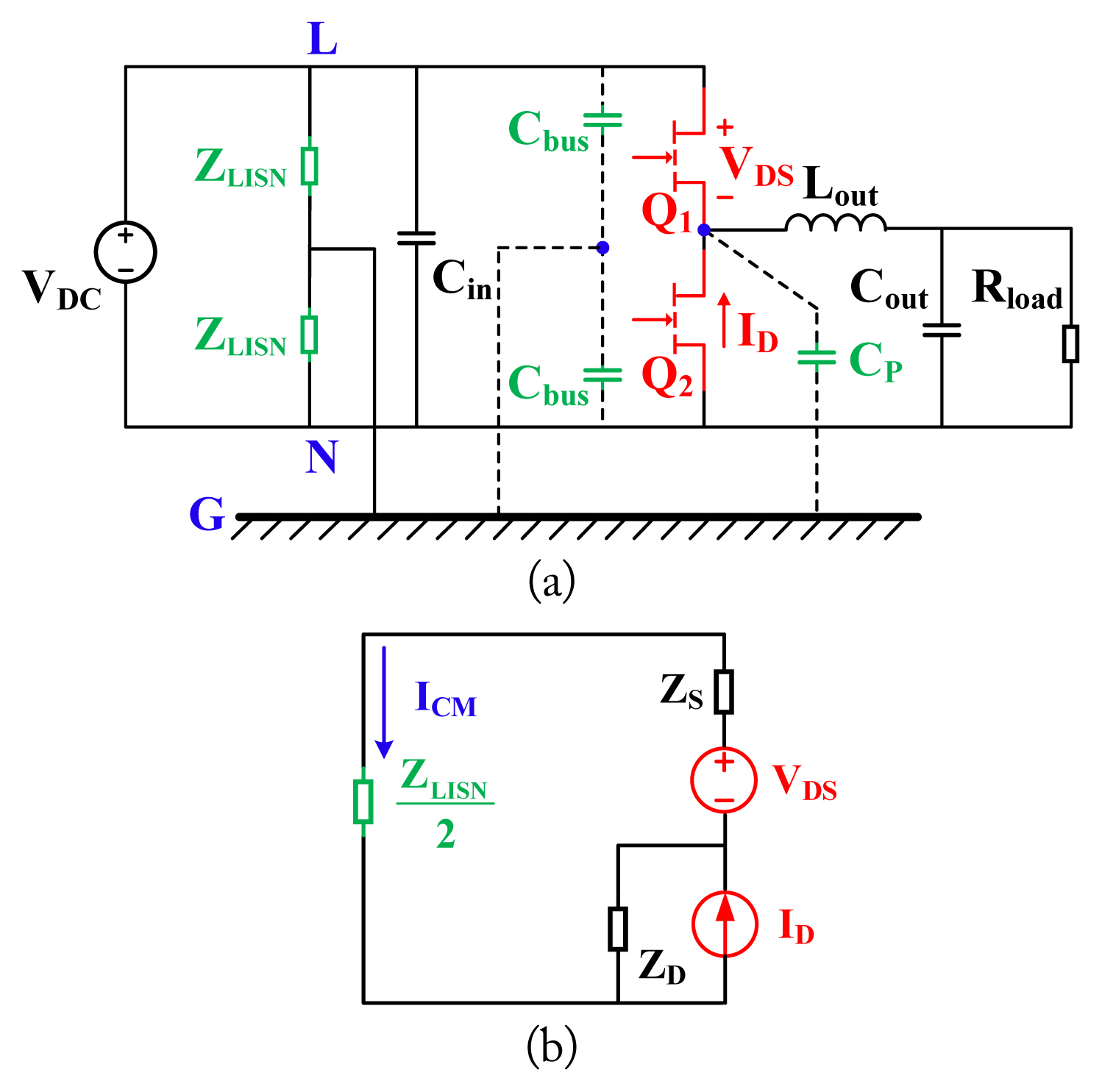
As illustrated in Fig. 1, a standard line impedance stabilization network (LISN) provides DC power to a synchronous buck converter, which is connected to the earth ground through the RL-CL and RN-CN branches. CP denotes the parasitic capacitance between the source of the GaN HEMT device and the heat sink of the half bridge. Owing to high-frequency switching of the HEMT device, significant dv/dt and di/dt are generated in the phase-leg node M, which is coupled to the ground through CP, leading to the generation of CM conducted noise. Here, because the packages used for the HEMTs are identical and the heat sink, as a whole, is fixed under the device, we can ignore the asymmetry of the conduction path and assume that the parasitic capacitances CP of the device to the ground are identical. Cbus1 and Cbus2 represent the parasitic capacitances between the alignments of positive and negative DC power on the PCB and the earth ground. Generally, these capacitances can be considered identical because they are composed of the same material and have the same alignment lengths.

Common mode (CM) EMI in GaN HEMT synchronous buck converter.
Notably, it is difficult in practice to completely isolate the output filter unit and the load side of converter from the ground. Therefore, the parasitic capacitance CPload to the earth ground on the output side should be considered when analyzing the CM conduction path.
During operation of the GaN HEMT synchronous buck converter, energy conversion is achieved by alternately switching on and off the upper and lower HEMTs. When the converter is operated in the on state, control device Q1 is turned on, synchronous device Q2 is turned off, and the power supply charges inductor Lout, which converts electrical energy into magnetic energy and stores it in the magnetic core. The switching speed of GaN HEMTs is generally of the order of tens of nanoseconds, during which time the potential at point M increases rapidly to the input voltage. Therefore, in the on state, the voltage VDS across the drain-source terminal of control device Q1 is the noise source. Similarly, when the converter is operated in the off state, control device Q1 is turned off, synchronous device Q2 is turned on, and the magnetic energy stored in inductor Lout is discharged as electrical energy to form a continuous loop through synchronous device Q2. Therefore, in the off state, the drain current ID of synchronous device Q2 is the noise source. because of the parasitic parameters in the CM EMI propagation paths, the voltage source VDS and current source ID produce the CM noise that flows through CP and Cbus to the earth and returns through the RL-CL and RN-CN branches.
Additional CM EMI noise sources include high dv/dt and di/dt, as well as high-frequency harmonic signals on the output side. However, because of the relatively strong ripple control requirements on the output side of the buck converter, which generally does not exceed 2% of the output voltage, and the isolation effect of the filter inductor Lout on the high-frequency signals, most of the switching noise is isolated in the phase-leg node M. Therefore, the contribution of the output side to the CM EMI in the buck converter is considered minimal, and the EMI-related problems caused by Q1 and Q2 are mainly considered and analyzed herein. Moreover, the drain-source voltage VDS across Q1 and drain current ID through Q2 can be considered to contain all CM EMI noise source information pertaining to the converter system. Based on the above analysis, the CM EMI loops in the GaN HEMT synchronous buck converter are as follows: VDS of Q1, ID of Q2, RL-CL, RN-CN, and parasitic capacitance branches Cbus and CP.
2. Equivalent Circuit of EMI Noise Source and CM Propagation Paths
To understand the CM EMI in a GaN HEMT synchronous buck converter, we propose a behavioral model of CM EMI noise in this section. The magnitude of the CL and CN illustrated in Fig. 1 is 0.1 μF, while the capacitance of Cin is high at several hundred microfarads to obtain a good filtering function for the input voltage. At a given frequency, the impedance of Cin is considerably smaller than those of CL and CN. Therefore, the positive and negative terminals L/N can be simplified as one node in the two-terminal model of the buck converter, as illustrated in Fig. 2.

Equivalent circuit of EMI noise source and CM propagation paths in GaN HEMT synchronous buck converter.
Fig. 2 shows the GaN HEMT buck converter and its equivalent CM EMI noise source circuit and CM propagation paths. The positive, negative, and ground input terminals of the GaN HEMT synchronous buck converter are labeled L, N, and G, respectively. According to the definition of CM EMI, the upper terminal of the equivalent circuit represents the input-side positive and negative terminals that are short-circuited together, which is referenced to ground. When the upper GaN HEMT Q1 is turned on, and the lower GaN HEMT Q2 is turned off, a high dv/dt voltage slew rate is produced on the drain-source voltage VDS of GaN HEMT Q1. Conversely, a high di/dt current slew rate is generated on the drain current ID of GaN HEMT Q2. Therefore, during the switching transient process, the upper GaN HEMT is modeled as the voltage source VDS and impedance ZS in series, according to Thevenin’s theorem, and the lower GaN HEMT is modeled as the current source ID and impedance ZD in parallel, according to Norton’s theorem.
III. CM EMI Behavioral Modeling Procedure
This section presents the CM EMI behavioral modeling procedure under the assumption that the GaN HEMT synchronous buck converter operates in a linear and time-invariant fashion at its input terminals [17]. The modeling procedures are designed using the nominal case and attenuated case, respectively, where the load impedance ZLISN is in parallel without or with a shunt impedance ZSHUNT.
Typically, the CM current signal is measured for the nominal case depicted in Fig. 3. The CM load of the model in this case is the LISN. As illustrated in Fig. 3(a), the LISN is modeled as a load impedance ZLISN, and the drain-source voltage VDS of the upper HEMT and drain current ID of the lower HEMT are modeled as CM EMI noise sources. According to Thevenin’s and Norton’s theorems, these two noise sources can be equated to a voltage source VDS in series with an impedance ZS and a current source ID in parallel with an impedance ZD, respectively, to obtain the equivalent circuit of the approximate model, as illustrated in Fig. 3(b). In this manner, the characteristics of the CM noise source are contained in VDS and ID, and the parasitic characteristics of the noise conduction path are contained in ZS and ZD.
Nominal case of model extraction: (a) generalized behavioral model and (b) approximate equivalent circuit.
The expression of the CM current can be obtained by applying the superposition theorem to the approximate equivalent circuit, as follows. The current source ID is first open-circuited to consider the effect of the drain-source voltage VDS of the upper GaN HEMT on the CM current in the loop, which corresponds to the “on” operating state of the buck converter, as illustrated in Fig. 4(a). Then, the voltage source VDS is short-circuited to consider the drain current ID of the lower GaN HEMT with respect to the CM current, which corresponds to the “off” operating state of the buck converter, as illustrated in Fig. 4(b).
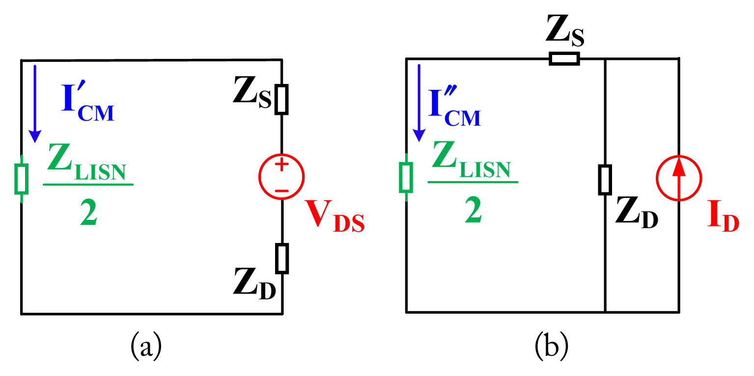
Equivalent circuit of ICM obtained by applying the superposition theorem: (a) equivalent circuit with ID open-circuited and (b) equivalent circuit with VDS short-circuited.
Fig. 4(a) depicts the “on” state of the buck converter, which represents the relationship between the upper GaN HEMT drain-source voltage VDS and the CM current
Fig. 4(b) corresponds to the “off” state of the buck converter, which represents the relationship between the lower GaN HEMT drain current ID and the CM current ICM. The expression for determining
By summing
To determine the model impedances ZD and ZS, more equations should be developed for attenuated cases by adding the shunt impedances ZSHUNT1 and ZSHUNT2 between L/N and G. Thus, the CM loads of the model in the attenuated cases can be written as
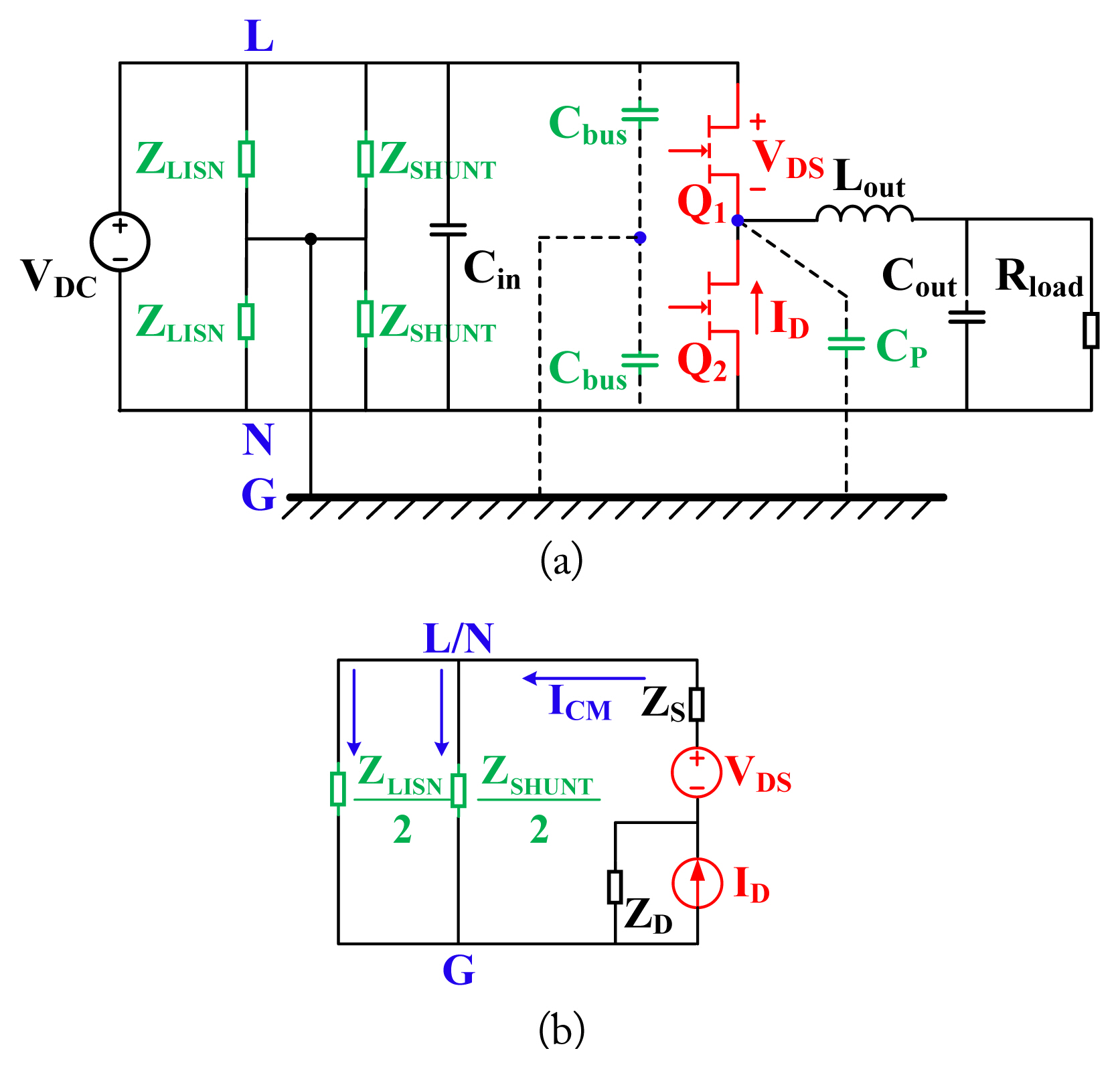
Attenuated case for model extraction: (a) generalized behavioral model and (b) approximate equivalent circuit.
Similar to the treatment of the nominal case, the approximate equivalent circuit corresponding to the attenuated case is first obtained (Fig. 5(b)). Then, the expressions of the CM current ICM1 and its corresponding equivalent circuit are obtained by applying the superposition theorem, and they are given in Eq. (4) and presented in Fig. 6.

Equivalent circuit of ICM1 obtained by applying the superposition theorem: (a) equivalent circuit with ID open-circuited and (b) equivalent circuit with VDS short-circuited.
Similarly, Eq. (5), which represents ICM2, can be obtained by replacing ZSHUNT1 with ZSHUNT2.
The VDS, and ID in Eqs. (4) and (5) correspond to the drain-source voltage VDS of the upper GaN HEMT and drain current ID of the lower GaN HEMT, respectively. Because the drain-source voltage VDS of the upper GaN HEMT and drain current ID of the lower GaN HEMT are mainly determined by the duty cycle of the control signal, the switching frequency, input voltage level, parasitic capacitance of the device itself, parasitic inductance introduced by the package, parasitic inductance of the PCB alignment, and variation of the CM load impedance have little effect on them. Therefore, we can assume that VDS and ID are constant in the nominal and attenuated cases.
According to Eqs. (4) and (5), the impedances ZD and ZS of the CM EMI noise source shown in Fig. 3 can be determined using Eqs. (6) and (7), respectively.
Notably, the impedances ZD and ZS are functions of ICM1, ICM2, VDS, ID,
IV. Extraction of CM EMI Behavioral Model Parameters
1. Experimental Setup
Fig. 7 shows a schematic diagram of the experimental setup of the GaN HEMT synchronous buck converter. The synchronous buck converter operates with a 100-V DC input and 50-V DC output across a 20-Ω load, where the switching frequency f is 500 kHz, and the drive signal duty cycle of the converter D is 0.5. The input capacitor consists of two 150-μF electrolytic capacitors, one 3-μF film capacitor, and four 100-nF multilayer ceramic capacitors in parallel. Two GaN HEMTs (INN650D140A; Innoscience, Zhuhai, China) are used in the synchronous buck converter. A photograph of the corresponding GaN HEMT synchronous buck converter setup is presented in Fig. 8. The digital controller (DSP TMS320F28335; Texas Instruments, Dallas, TX, USA) provides pulse-width-modulated driving signals for the driver IC (STDRIVEG600; STMicroelectronics, Geneva, Switzerland) of the GaN HEMTs. The LISN used in the experiment (NSLK 8127; Rohde & Schwarz, Munchen, Germany) can operate between 9 kHz and 30 MHz. The CM currents ICM1 and ICM2 can be measured directly in the frequency range 10 Hz–7 GHz by using an equivalent series resistance (ESR) EMI test receiver (Rohde & Schwarz). The drain-to-source voltage VDS and current source ID of the GaN HEMTs are measured using a digital oscilloscope (DPO 5034B; Tektronix, Beaverton, OR, USA) with a bandwidth of 350 MHz, sampling rate of 5 GS/s, and four channels.
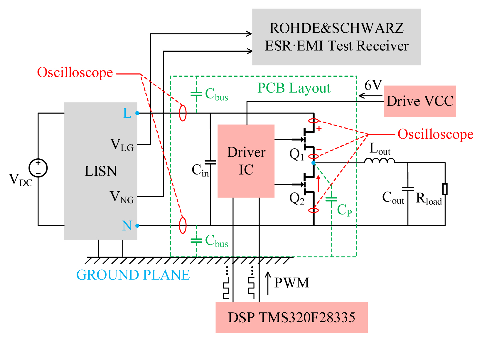
Schematic of experimental setup of a GaN HEMT synchronous buck converter.
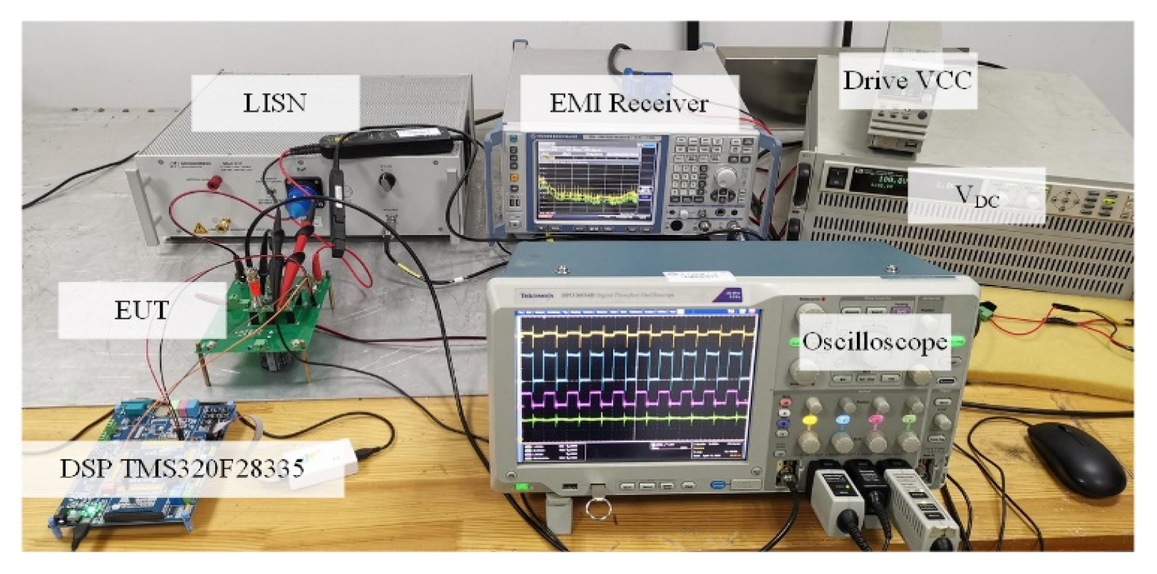
GaN HEMT synchronous buck converter setup.
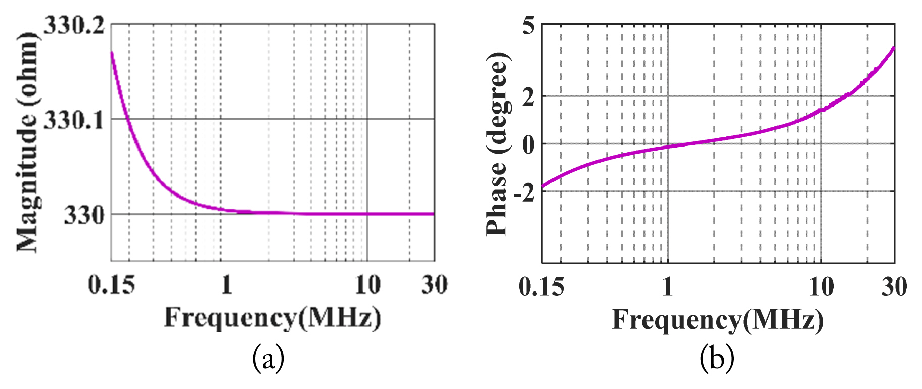
An LISN (NSLK 8127) is used in the experimental setup to block EMI noise from the DC source. The circuit schematic of this LISN and its corresponding photograph are depicted in Fig. 9. Then, the output impedances of the LISN are characterized using a WK6500B Series impedance analyzer, which is shown in Fig. 10. Interestingly, the output impedance of the LISN is inductive in nature in the 150 kHz–2 MHz frequency range, and it is 50 Ω in the 2–30 MHz frequency range.
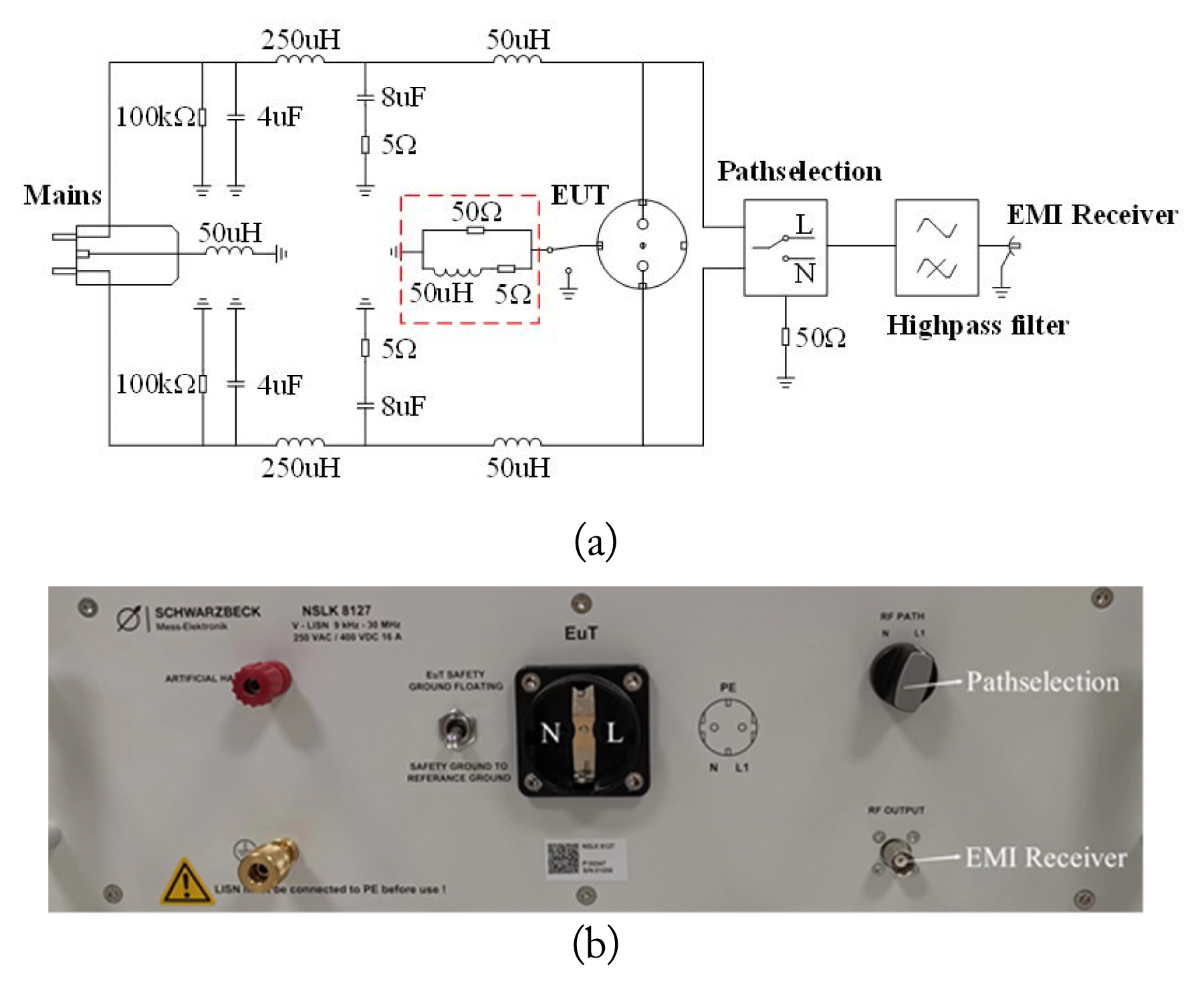
Line impedance stabilization network (LISN) used in the experimental setup: (a) circuit schematic and (b) photograph of LISN.

Impedance characteristic curve of ZLISN: (a) impedance magnitude and (b) impedance phase.
2. Extraction of Model Parameters
To obtain an accurate CM EMI noise model, the impedances of the CM EMI propagation paths are first determined by conducting experimental measurements. A series combination of a 22-Ω resistor and 0.1-μF capacitor is used as the shunt impedance ZSHUNT1. Another series combination of a 330-Ω resistor and 0.1-μF capacitor is used as the shunt impedance ZSHUNT2. Additionally, the shunt impedances ZSHUNT1 and ZSHUNT2 are measured using the WK6500B SERIES impedance analyzer, and the measured impedance curves of ZSHUNT1 and ZSHUNT2 are depicted in Figs. 11 and 12, respectively.

Impedance characteristic curve of ZSHUNT1: (a) impedance magnitude and (b) impedance phase.
Impedance characteristic curve of ZSHUNT2: (a) impedance magnitude and (b) impedance phase.
Second, the noise voltage and current sources, such as VDS and ID, are measured using the digital oscilloscope. The time-and frequency-domain waveforms of VDS are presented in Fig. 13. The experimental measurements of the noise current source ID are presented in Fig. 14.

Measured voltage VDS: (a) time-domain waveform of VDS, (b) magnitude of VDS in frequency domain, and (c) phase of VDS in frequency domain.
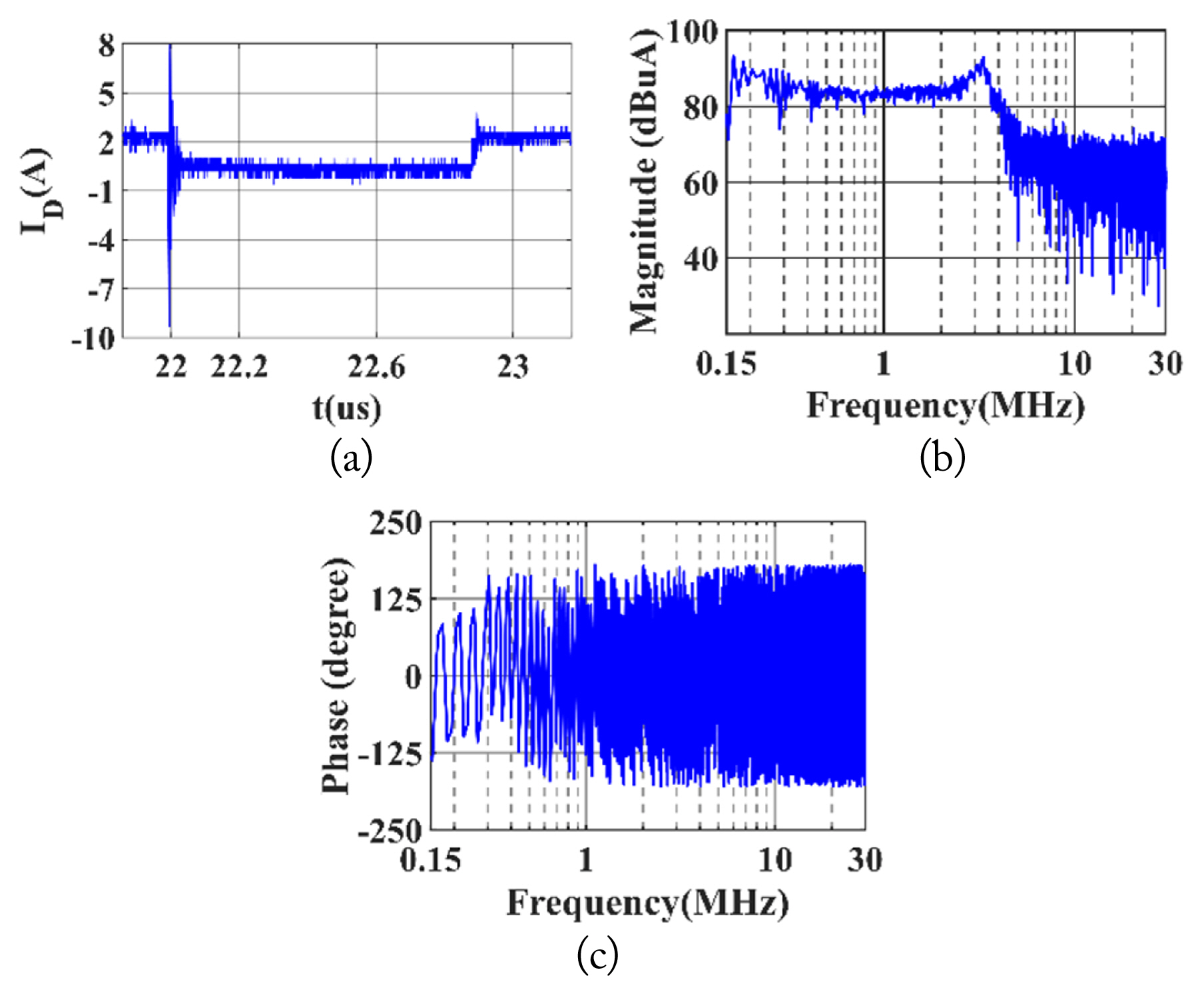
Measured current ID: (a) time-domain waveform of ID, (b) magnitude of ID in frequency domain, and (c) phase of ID in frequency domain.
The next step is to measure the CM EMI currents under different load impedance conditions. The characteristics of the CM EMI noise source are invariable, even though shunt impedances are applied between L/N and G, which changes the CM EMI loop impedance in the GaN HEMT synchronous buck converter. Then, the CM currents ICM1 and ICM2 are measured to calculate the model impedances ZD and ZS. Figs. 15 and 16 show the measured CM currents ICM1 and ICM2, respectively, with the shunt impedance ZSHUNT1 and ZSHUNT2 added between L/N and G parallel to ZLISN. Notably, higher ringing in the time-domain waveforms of the CM current can be seen in Figs. 15(a) and 16(a); these waveforms are related to the turn-on and turn-off switching processes of the GaN HEMTs, respectively. Moreover, according to Figs. 15(a) and 16(a), the magnitude of ringing during the turn-on process of the upper GaN HEMT is higher than that during the turn-off process. In addition, according to Figs. 15 and 16, the magnitude of the ICM2 spectrum is smaller than that of ICM1 at frequencies lower than 1 MHz. This is because the higher resistance value of ZSHUNT2 relative to that of ZSHUNT1 has a dampening effect on the CM EMI noise.
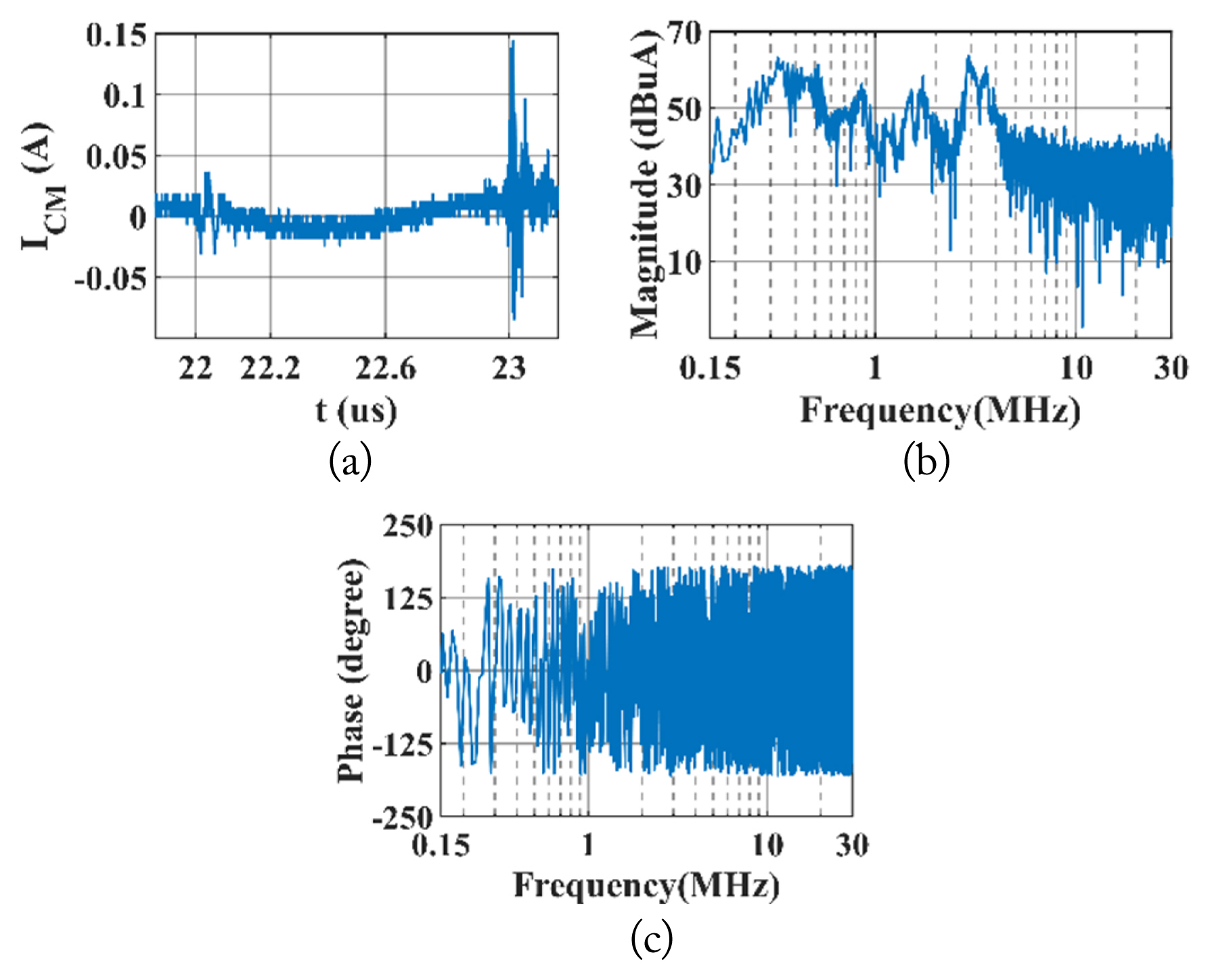
Measured CM current ICM1 with the shunt impedance ZSHUNT1: (a) time-domain waveform of ICM1, (b) magnitude of ICM1 in frequency domain, and (c) phase of ICM1 in frequency domain.
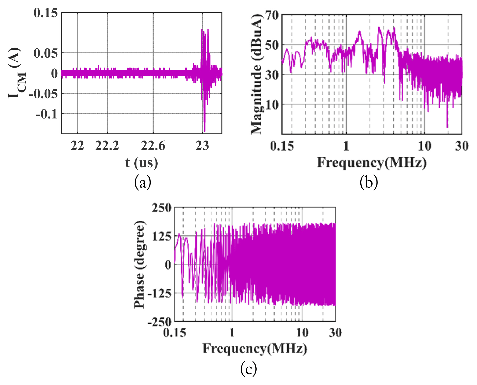
Measured CM current ICM2 with the shunt impedance ZSHUNT2: (a) time-domain waveform of ICM2, (b) magnitude of ICM2 in frequency domain, and (c) phase of ICM2 in frequency domain.
According to the experimental measurements, such as VDS, ID, ICM1 and ICM2, the impedances ZD and ZS in the CM EMI noise model can be calculated using Eqs. (6) and (7), respectively, as shown in Figs. 17 and 18. The entire modeling process is depicted in Fig. 19.
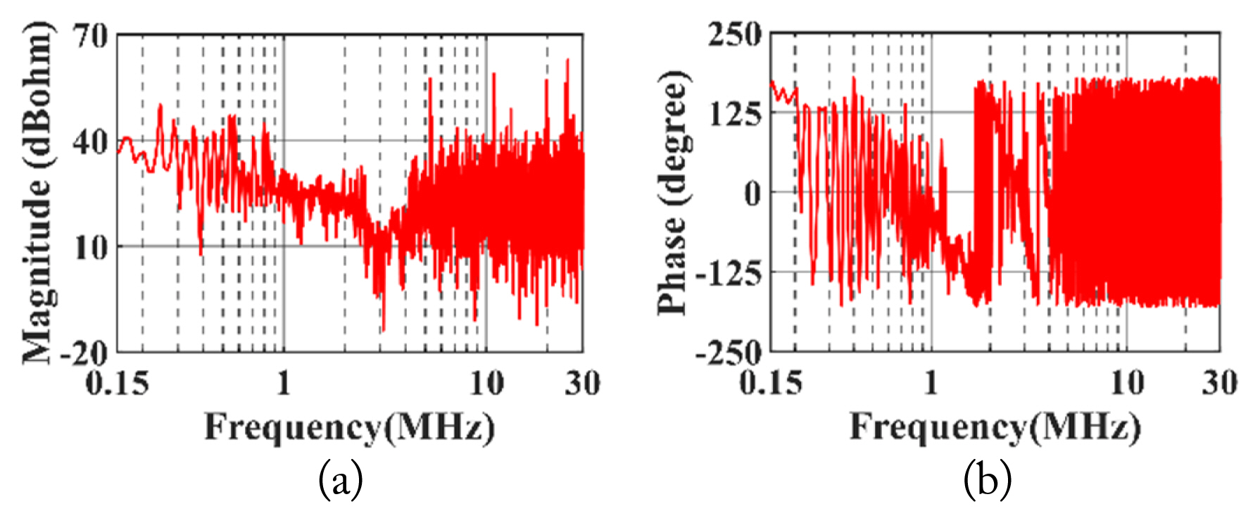
Calculated impedance ZD: (a) magnitude of ZD in frequency domain and (b) phase of ZD in frequency domain.
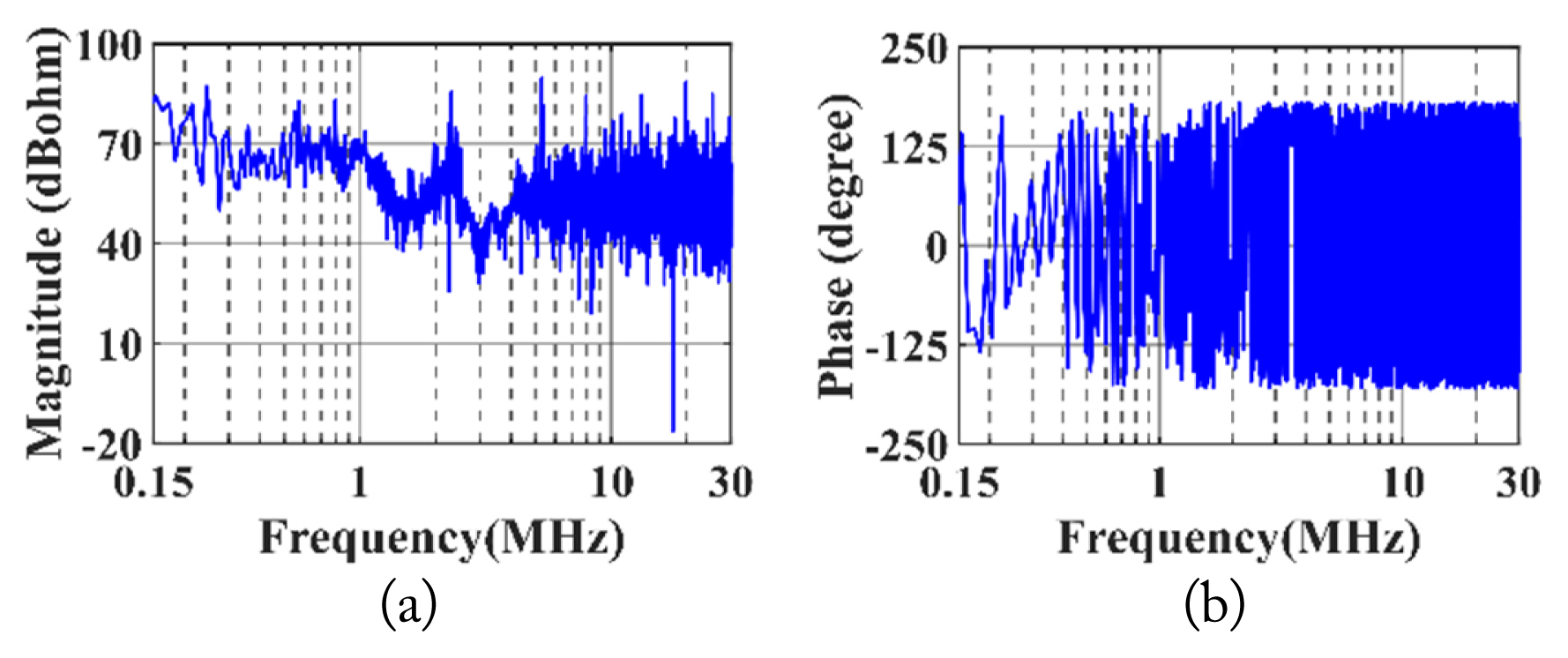
Calculated impedance ZS: (a) magnitude of ZS in frequency domain and (b) phase of ZS in frequency domain.
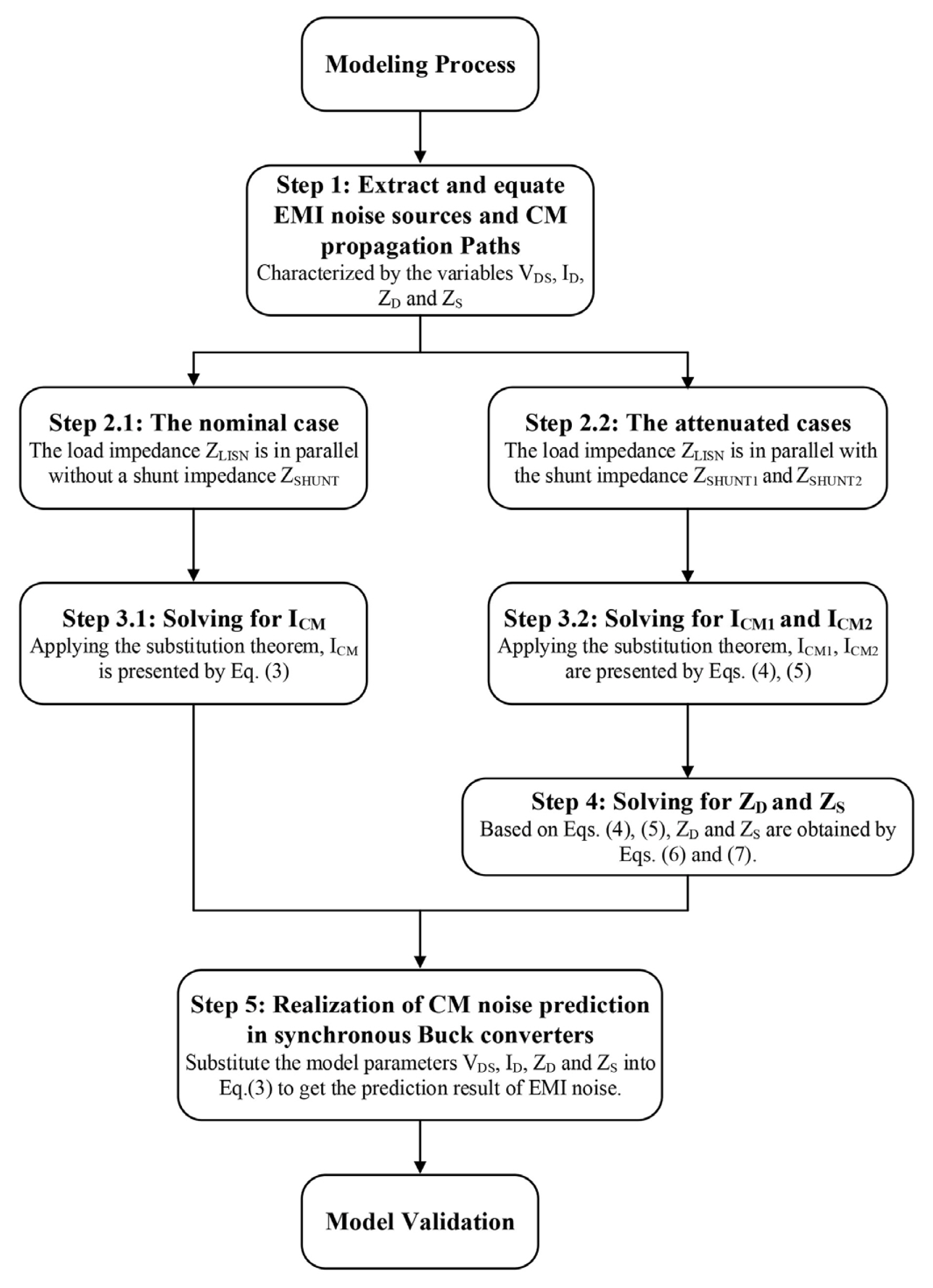
Block diagram of entire modeling process.
V. CM EMI Model Validation
The CM EMI behavioral model proposed in this paper was validated using a GaN HEMT synchronous buck converter. Note that we aimed to validate the CM EMI model for predicting the CM current in the GaN HEMT synchronous buck converter, and the EMC standards were excluded from the comparison between the experimental and calculated results. To predict the CM noise currents, the impedances ZD and ZS in the CM EMI noise model were determined, as illustrated in Figs. 17 and 18, respectively. The drain-source voltage VDS and drain current ID of the GaN HEMTs were measured, as shown in Figs. 13 and 14, respectively. Eq. (3) was then used to calculate the resulting CM current through the GaN HEMT synchronous buck converter. Notably, the CM current was measured considering the shunt impedances, as illustrated in Fig. 20. A comparison between measured and predicted CM currents is presented in Fig. 21.
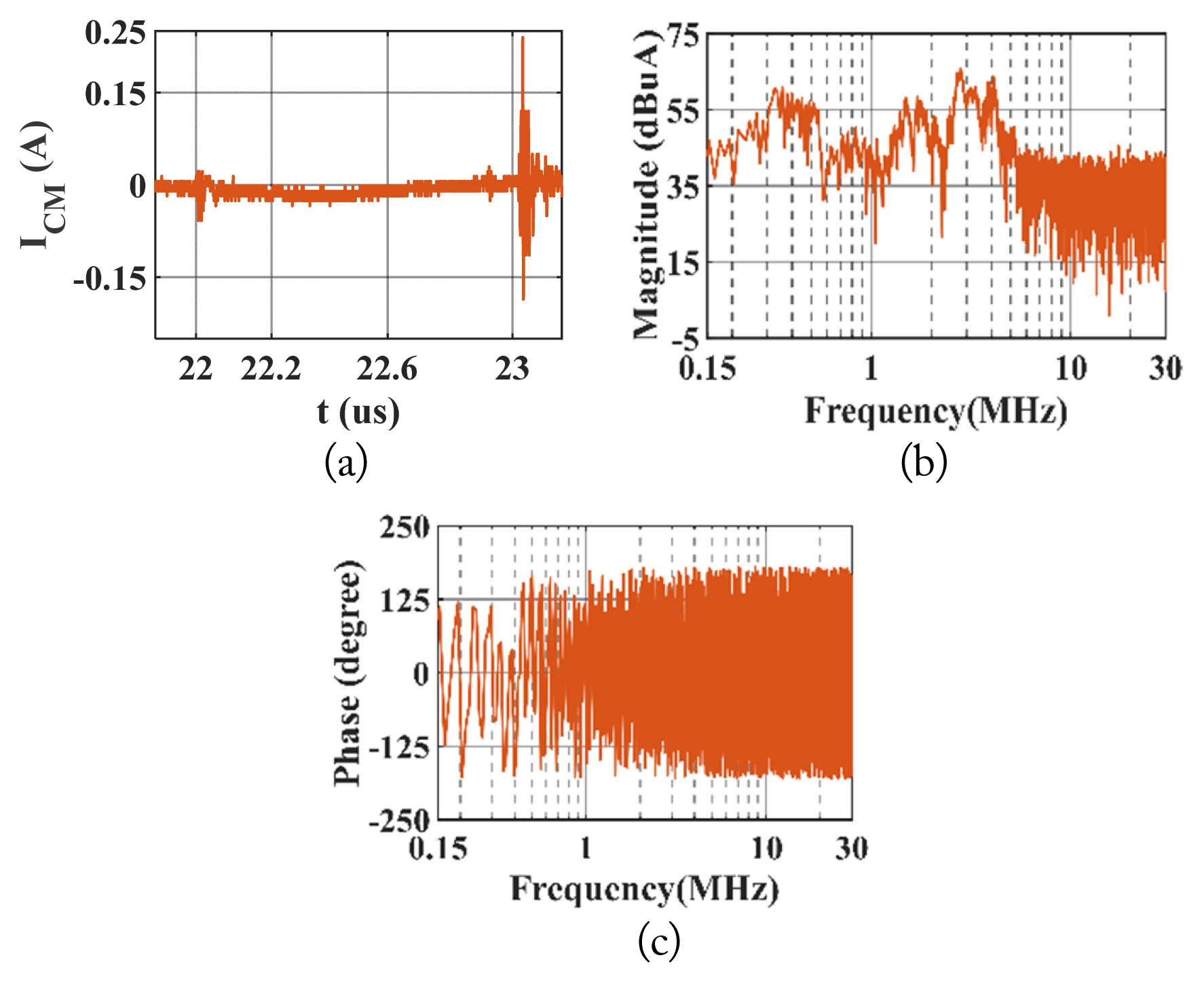
Measured CM current ICM without shunt impedance: (a) time-domain waveform of ICM, (b) magnitude of ICM in frequency domain, and (c) phase of ICM in frequency domain.
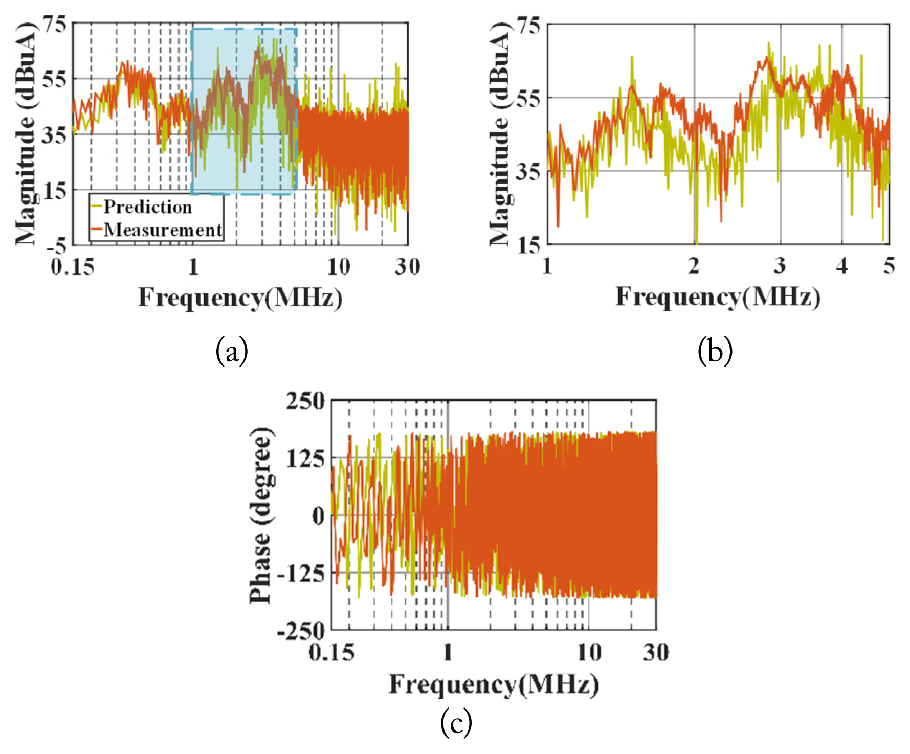
Comparison of measured and predicted CM currents of GaN HEMT synchronous buck converter operating at 500 kHz: (a) magnitude of CM currents in frequency domain, (b) magnified view of 1–5 MHz frequency range, and (c) phase of CM currents in frequency domain.
The CM EMI model was developed using two impedances, a voltage source, and a current source, and it was difficult to include all these components in the physic system. Thus, a few spikes were observed in the 1–5 MHz frequency range, which were different from the experimental results. Furthermore, the instruments used in the EMI tests, including the LISN, EMI receiver, oscilloscope, and various probes, introduced a few unavoidable errors, which had a certain impact on the prediction accuracy of the CM EMI model. According to Figs. 12 and 13, the characteristics of ZSHUNT1 and ZSHUNT2 were affected by the parasitic parameters in the higher-frequency bands (greater than or equal to 10 MHz). This explained the appearance of a few spikes in the comparison results at frequencies higher than 5 MHz in Fig. 21. However, in general, the proposed CM EMI behavior model was accurate and reliable in predicting the CM EMI current.
VI. CM EMI Prediction under Different Switching Frequencies
To demonstrate the accuracy of the proposed CM EMI behavioral model in terms of predicting the CM EMI noise in the GaN HEMT synchronous buck converter, the CM currents through the system were measured in the 200 kHz and 100 kHz switching frequency cases, as illustrated in Figs. 22 and 23, respectively. Both the magnitude and phase of the CM current spectra predicted using the behavioral model were compared with the corresponding experimental measurements. The predicted CM noise matched well with the experimental results in the 150 kHz–30 MHz frequency range.
Comparison of measured and predicted CM currents of GaN HEMT synchronous buck converter operated at 200 kHz: (a) magnitude of CM currents in frequency domain and (b) magnified view of the 1–5 MHz frequency range.

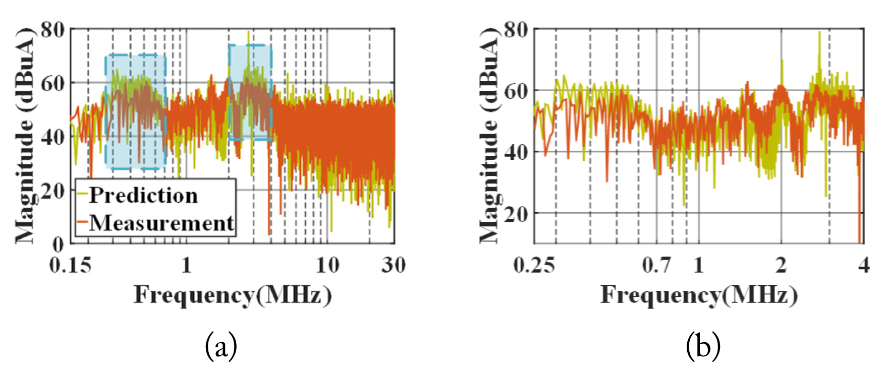
Comparison of measured and predicted CM currents of GaN HEMT synchronous buck converter operated at 100 kHz: (a) magnitude of CM currents in frequency domain and (b) magnified view of the 1–5 MHz frequency range.
As can be inferred from Fig. 22, several peaks exhibited larger magnitude differences when the GaN-based converter was operated at 200 kHz because of the deviations between the measured and calculated values of the impedances ZD and ZS. The maximum deviation was approximately 5 dB in the 300–700 kHz and 1–4 MHz frequency ranges. Notably, the predicted magnitude of the CM current spectrum was higher than the measured magnitude at frequencies lower than 1 MHz owing to the effect of the LISN impedance in the 150 kHz–1 MHz frequency range.
Fig. 23, by contrast, shows that the CM EMI noise model was able to predict the CM currents with good accuracy at frequencies lower than 10 MHz in the 100 kHz switching frequency case. The maximum deviation was approximately 4 dB in the 250–500 kHz and 2–4.5 MHz frequency ranges. The comparison results are remarkably different at frequencies higher than 10 MHz owing to the accuracy of the experimental measurements in the high-frequency range and the interference due to environmental noise.
The deviation in the comparison results can be summarized as follows:
In the process of predicting CM EMI noise, it is inevitable to ignore the contribution of the PCB layout basics, passive devices, active devices, and DSP controller to the EMI. However, the above factors do influence the experimental results.
The parasitic parameters of the two shunt impedances ZSHUNT1 and ZSHUNT2 in the high-frequency band inevitably introduce some interference in the calculation of the model parameters.
The accuracy of the measurement equipment in the high-frequency range and the interference due to environmental noise affect the experimental results to some extent.
In general, the CM EMI behavioral model proposed herein can be used to analyze and predict the EMI noise in the GaN HEMT synchronous buck converter.
VII. Conclusion
A CM EMI behavioral model was proposed to predict the CM current through a GaN HEMT synchronous buck converter, which consisted of a voltage source, current source, and two impedances. First, we devised an experimental setup for extracting model parameters. Then, we measured the drain-source voltage VDS and drain current ID of GaN HEMTs and estimated the impedances of the CM EMI noise model by conducting experimental measurements. Thereafter, we determined the parameters of the CM EMI model to predict the CM EMI current through the system, where experimental validation was performed using a GaN HEMT synchronous buck converter.
The proposed behavioral model and prediction method can help EMC engineers to evaluate and predict the CM EMI of a GaN HEMT synchronous buck converter by using simple experimental data. To a certain extent, the proposed model solves the time-consuming and complex problem of traditional EMI testing. Furthermore, the investigation results can provide EMC engineers with an optimum method to design EMI filters for GaN-based power converters.
Acknowledgments
This study is supported by the Science and Technology Program of State Grid Co., LTD (Grant No. 5700-2022 17209A-1-1-ZN).
References
Biography

Chuang Bi earned a Ph.D. in Electrical and Electronic Engineering from University College Dublin, Dublin, Ireland, in 2012. He joined School of Astronautics and Aeronautics and Aircraft Swarm Intelligent Sensing and Cooperative Control Key Laboratory of Sichuan Province, University of Electronic Science and Technology of China, Chengdu, China, in 2016, where he is currently an Associate Professor. His research interests include power electronics, electromagnetic compatibility, and active EMI filters.

Heyang Shan received a B.S. in Communication Engineering from Taiyuan University of Technology, Taiyuan, China, in 2020. He is currently working toward an M.S. in Electronic Information at University of Electronic Science and Technology, Chengdu, China. His research interests include DC-DC converters and EMI issues in GaN systems.
Kai Gao completed B.S. and Ph.D. in Electrical Engineering from Tsinghua University, Beijing, China, in 1997 and 2002, respectively. He is currently a Professor of Engineering with the Electric Power Research Institute, State Grid Shanghai Municipal Electric Power Company, Shanghai, China. His research interests include condition sensing, smart monitoring, and diagnosis of power equipment.

Shaojing Wang received an M.S. from Shanghai Jiaotong University of Electrical Engineering, Shanghai, China, in 2017. She is currently a professional engineer with State Grid Shanghai Electric Power Research Institute, Shanghai, China. She has published over 20 papers, been awarded two patents, and formulated an enterprise standard. Her research interests include detection and evaluation of power equipment and smart sensing of power.

Peng Xu received an M.S. from Shanghai Jiaotong University of High Voltage Technology, Shanghai, China, in 2006. He is currently employed as a Vice Director by State Grid Shanghai Electric Power Research Institute, Shanghai, China. He is a member of CIGRE SC A3. He has published over 20 papers, been awarded more than 10 patents, and formulated nine standards. His research interests include the detection and evaluation of power equipment, smart sensing technology, and high-voltage test technology.