


I. Introduction
A branch-line coupler is one of the key components in RF/microwave systems and is widely used in balanced mixers, balanced amplifiers, and power dividers. A 3 dB branch-line coupler offers an equal amplitude power division and a 90° phase shift between the two outputs. The conventional branchline coupler consists of four quarter-wavelength transmission lines and offers a single passband. Several methods have been utilized to realize harmonic suppression in single-band branchline couplers [1–7]. In [1], a coupled-line section was used to achieve a compact size and spurious rejection. Multiple asymmetric π-shaped structures [2] and H-shaped structures [3] were utilized to realize a compact size and harmonic suppression. Resonators with an interdigital structure [4], radial-shaped resonators [5], closed-loop, open-loop resonators [6], and stepped impedance resonators [7] have been used to achieve the proposed couplers. In [8–13], dual-band branch-line couplers were proposed. Shunt open-circuit dual composite right/left-handed cells [8], π-shaped lines [9], coupling lines [10], cross-coupling branches [11], and port extensions [12] have been used to achieve dual-band couplers. A compact dual-band coupler using feature-based optimization was proposed in [13].
In this study, a dual-band branch-line coupler with ultra-wideband harmonic suppression is proposed. Based on the conventional branch-line coupler structure, a novel dual-band coupler with π-shaped lines and frequency-selecting coupling structure (FSCS) is proposed with the equivalent circuit. The related theory analysis verifies that the proposed design features ultra-wideband harmonic suppression. To validate the theory, a coupler with operating frequencies of 0.9 GHz and 2.0 GHz was simulated, fabricated, and characterized.
II. Analysis and Design
1. Analysis of the Dual-Band Coupler Design
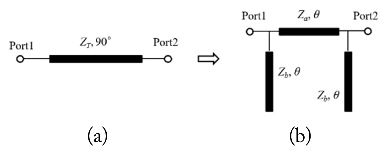
A quarter-wavelength transmission line with a characteristic impedance of ZT is replaced with a π-shaped line, as shown in Fig. 1. The characteristic impedances of the center transmission line and two open stubs are Za and Zb, respectively. The electrical length of the center transmission line and the two open stubs are the same to reduce the size. The ABCD matrices can be used to drive the parameter relationship between the quarter-wavelength transmission line and the π-shaped line, which is given by:
By solving Eq. (1), we obtain.
Eq. (2) can be solved as θ = θ1 and θ = θ2 to be its first two positive solutions, where θ1 and θ2 are the corresponding electrical lengths at the operating frequencies of the lower (f1) and upper (f2) bands, respectively. The relationship between θ1 and θ2 can be expressed as
By setting a as:
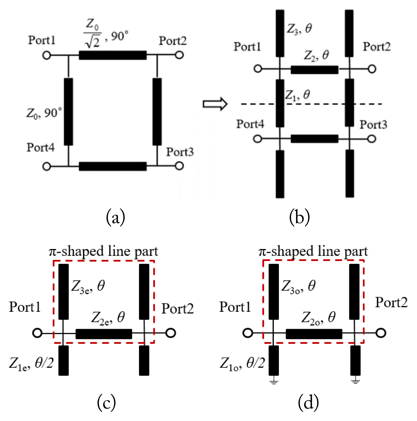
Fig. 2(b) depicts the dual-band coupler with the π-shaped line that evolved from the conventional coupler in Fig. 2(a) by using the substitution depicted in Fig. 1. Because of its symmetric structure, the even- and odd-mode methods can be used to analyze the π-shaped line coupler. It’s even- and odd-mode circuits are shown in Fig. 2(c) and 2(d). The ABCD matrix of the even-mode circuit is given by
where P1 is the matrix of the π-shaped line part shown in Fig. 2(c) (dashed line) and simplified as Eq. (1), and P2 is given by
The ABCD matrix of the odd-mode circuit is
where P3 is the matrix of the π-shaped line part shown in Fig. 2(d) (dashed line), and
The S-parameters of the coupler related to the even and odd modes are as follows [14]:
where Γe,o and Te,o are the even- and odd-mode reflection and transmission coefficients, respectively. Thus, Γe,o and Te,o are given by
At the center frequency of f0 = (f1+f2)/2, S21 = 0. The electrical length (θ) at f0 can be solved from Eqs. (8), (9), and (10b) and then given by
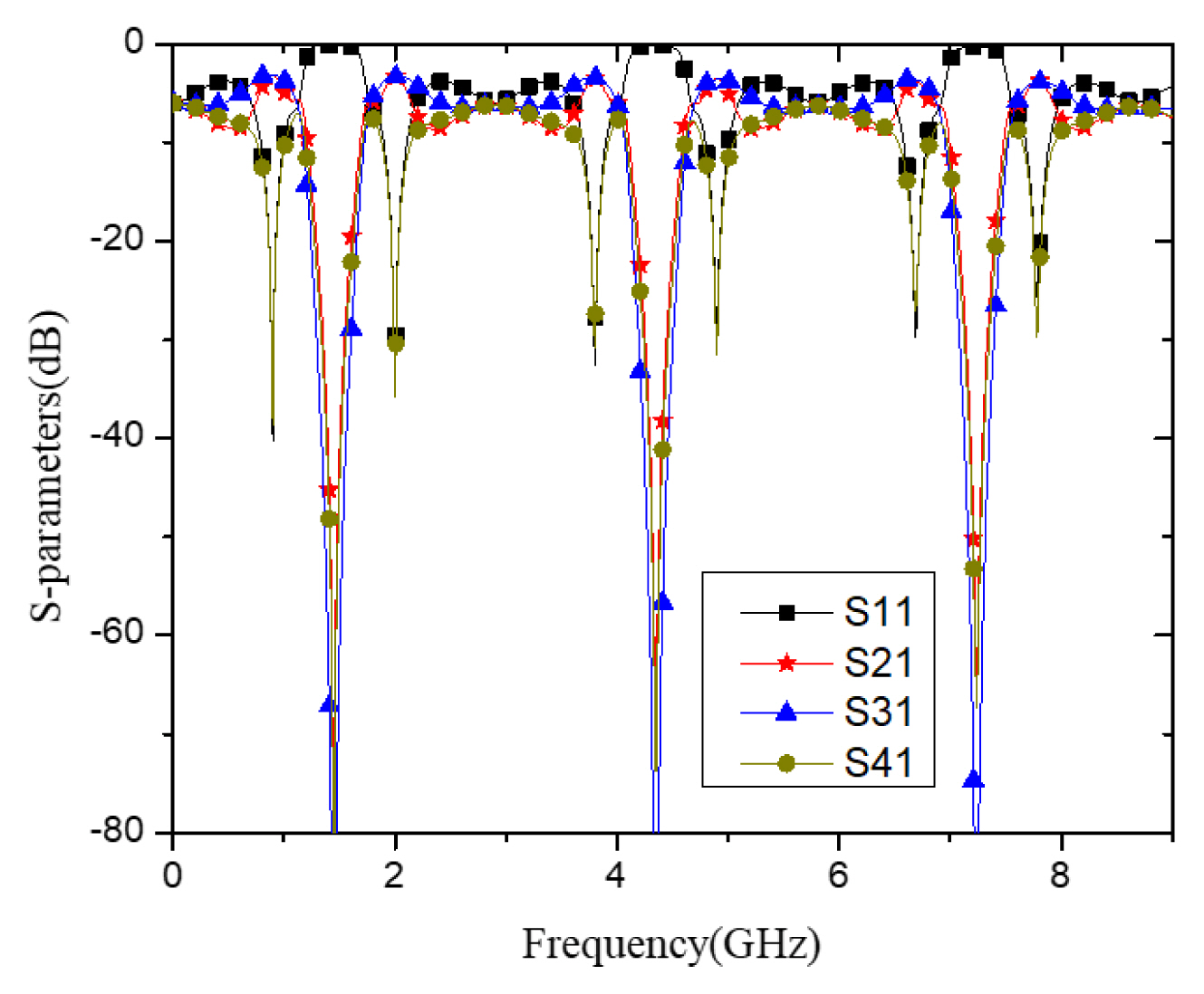
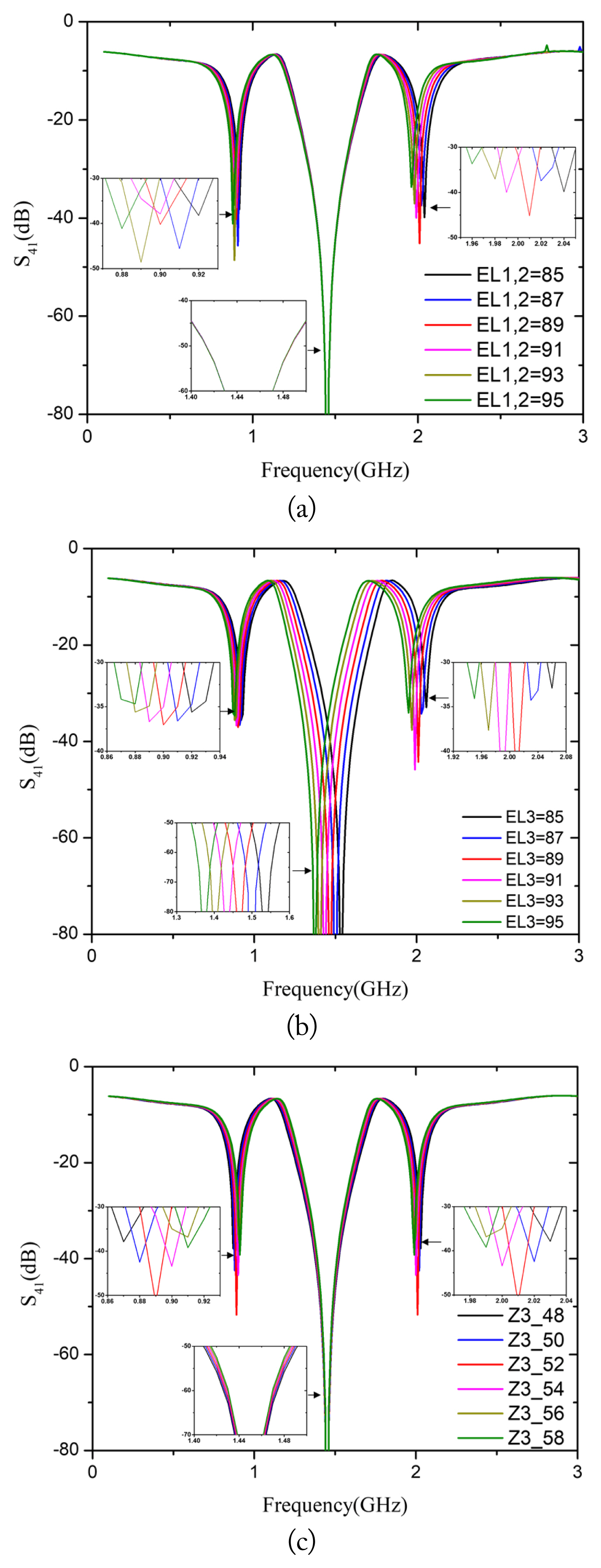
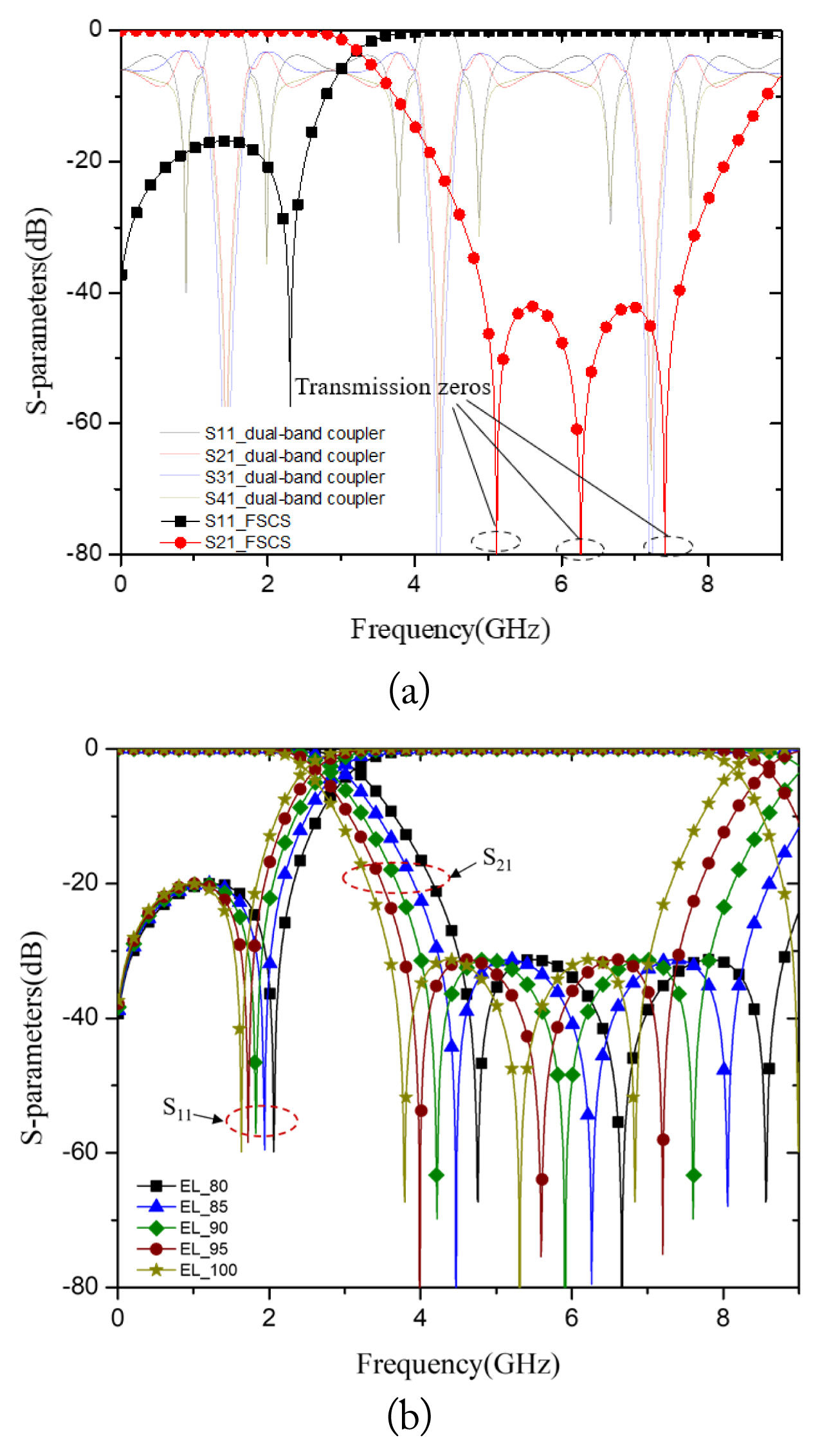
In this work, m = 0 is chosen to realize a compact size, and the length of all transmission lines and stubs in Fig. 2(b) is π/2. At f1 = 0.9 GHz, f2 = 2 GHz, and f0 = 1.45 GHz are set, and the values of Z1, Z2, and Z3 are 42.8 Ω, 60.5 Ω, and 54.4 Ω calculated with Eqs. (6) and (7), respectively. The simulation results for the dual-band coupler depicted in Fig. 2(b) with the parameters described above are shown in Fig. 3. The dual-band coupler operates at 0.9 GHz and 2 GHz. The effects of the coupler geometric characteristics, including the electrical length (EL1,2 and EL3) of the transmission line with impedances of Z1, Z2, and Z3, and the impedance (Z3) in Fig. 2(b) are shown in Fig. 4. In Fig. 4(a), f1 and f2 decrease as EL1,2 increases from 85° to 95°, while f1 is maintained. f0, f1, and f2 clearly decrease as EL3 increases from 85° to 95°, as shown in Fig. 4(b). In Fig. 4(c), f1 increases slightly, and f2 decreases somewhat as Z3 increases from 48 to 58 Ω; meanwhile, f0 is almost unchanged.
2. Analysis of the Harmonic Suppression Component
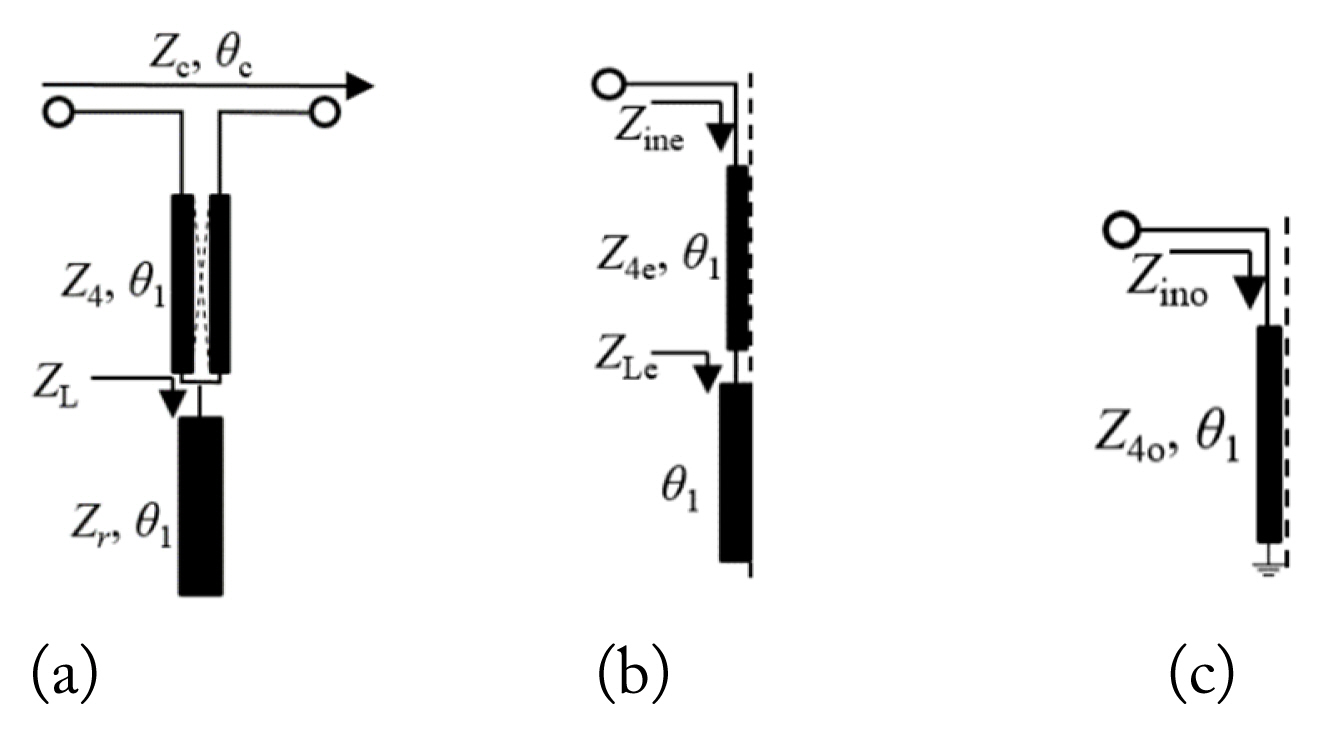
The harmonic suppression characteristic is supplied by FSCS with two transmission lines [15]. Fig. 5(a) depicts one FSCS unit with the equivalent characteristic impedance of Zc and an equivalent electrical length of θc. The equivalent even- and odd-mode circuits are shown in Fig. 5(b) and 5(c). At the center frequency (fs) of the stopband, the electrical length, θ1 = π/2. The input impedances of the even and odd modes can be derived as:
For the FSCS depicted in Fig. 5(a), the transmission coefficient S21 is given by
where Γe and Γo are the reflection coefficients, Zine and Zino are the input impedance of the even- and odd-mode excitations, and Z0 is the system impedance.
For transmission zero, S21 = 0. By calculating Eqs. (13) and (14), the created transmission zeros are achieved at frequencies θ = π/2 and θ = (π/2) ± Δθ. In addition, the simulation result of one FSCS cell with the results for the dual-band coupler proposed in the previous section are shown in Fig. 6(a). The signal of the dual-band coupler will pass in the passband of the FSCS, while the signal will be rejected in the stopband of the FSCS. The FSCS provides an ultra-wide bandwidth by generating three transmission zeros in the stopband [16]. The S-parameters of the FSCS with varying electrical length (EL), which is represented as θ1 in Fig. 5, are shown in Fig. 6(b). The position of the pole and the three transmission zeros can be tuned by changing the length of the FSCS, which means that the position and range of the stopband of the proposed coupler are controllable.
The equivalent characteristic impedance Zc and the equivalent length θc of the FSCS in the passband can be derived as
Note that the values of Zc and θc are meaningful only beyond the stopband.
For the equivalent characteristic impedance Zc =Z1 = 42.8 Ω and the equivalent length θc =θ = π/2 in Fig. 2(b), the even-mode impedance, odd-mode impedance, and the electrical length of the FSCS are 207 Ω, 133 Ω, and 13.6°, respectively. The impedance and electrical length of the open stub are 16 Ω and 7.6°, respectively. The impedance and electrical length of the compensate transmission lines on the two sides of the FSCS are 42.8 Ω and 14°, respectively. For another branch line, the equivalent characteristic impedance Zc = Z2 = 60.5 Ω and the equivalent length θc = θ = π/2 in Fig. 2(b), the even-mode impedance, odd-mode impedance, and the electrical length of the FSCS are 254 Ω, 85 Ω, and 14.2°, respectively. The impedance and the electrical length of the open stub are 34 Ω and 17°, respectively. The impedance and electrical length of compensate transmission lines on the two sides of the FSCS are 60.5 Ω and 6.4°, respectively.
III. Simulation and Measurement Results
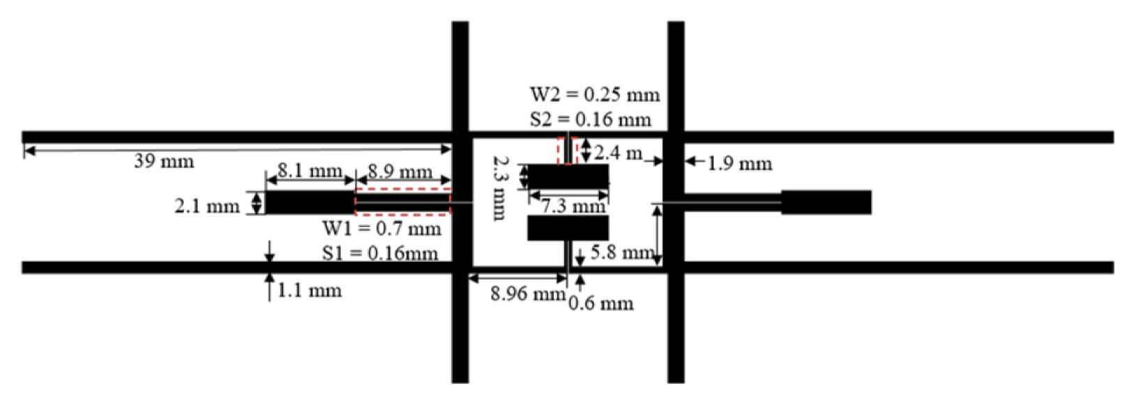
Based on the analysis of the circuit in Section II, a dual-band coupler with π-shaped lines and harmonic suppression components is presented. The layout of the proposed coupler and the size information are shown in Fig. 7. The phase difference between S21 and S31 is depicted in Fig. 8. The proposed dual-band coupler is designed on a Teflon substrate with a relative dielectric constant of 2.54, a thickness of 0.54 mm, and a copper thickness of 0.018 mm. The coupler is simulated using the ANSYS Electronics Desktop (HFSS), and the measurement is performed with an Agilent Vector Network Analyzer (VNA) 8719ES. Fig. 9 shows a photograph of the proposed coupler. The electrical size of the proposed coupler is 0.79λg × 0.1λg, and the whole circuit is 99.06 mm × 12.96 mm.
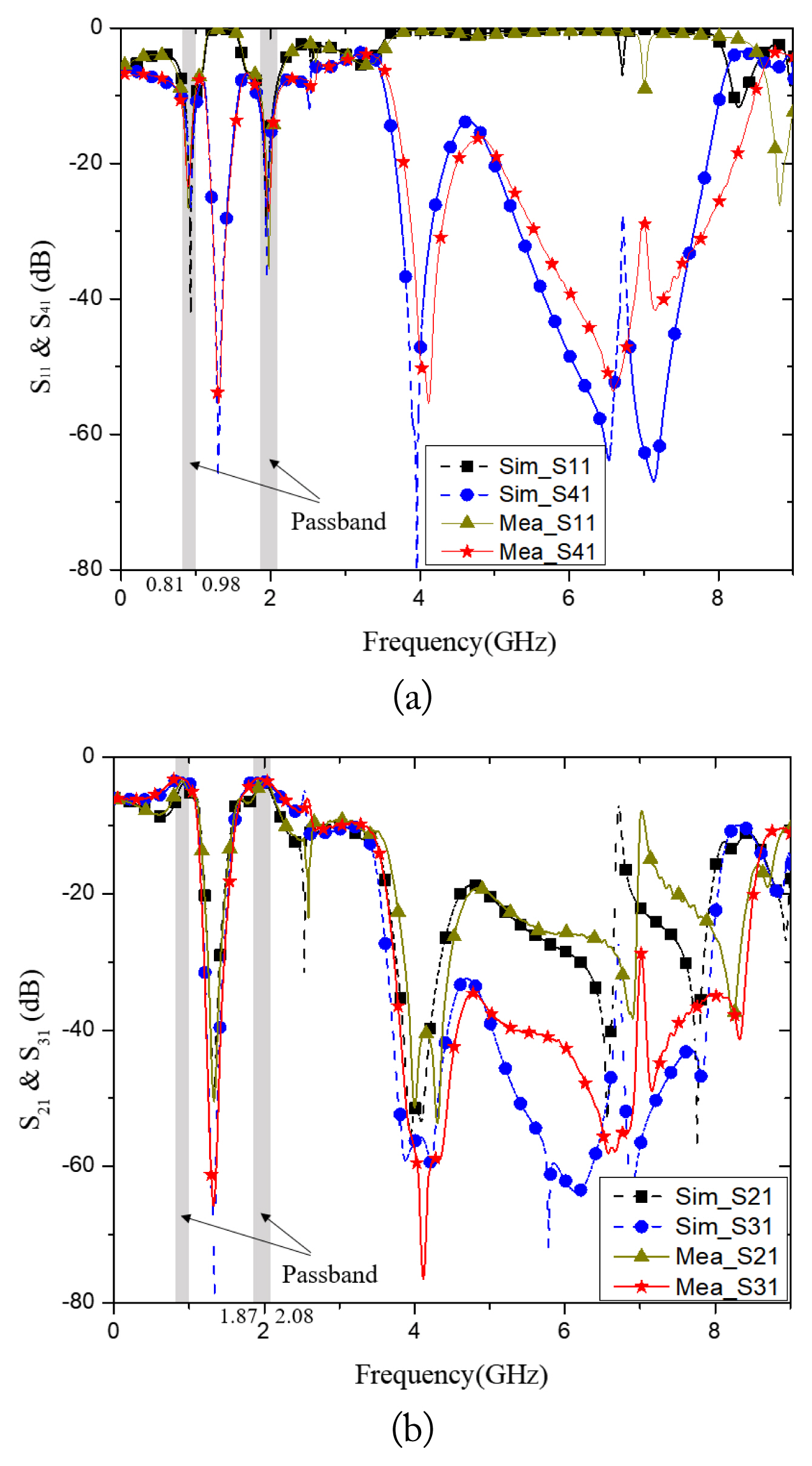
The simulation and measurement results for the S-parameters are depicted in Fig. 10. The proposed dual-band coupler operates at 0.9 GHz and 2 GHz with a corresponding fractional −10 dB bandwidth of 18.9% and 10.5%, respectively. The insertion loss of S21 at 0.9 GHz and 2 GHz is −3.5 dB and −3.4 dB, respectively, while the insertion loss of S31 at 0.9 GHz and 2 GHz is −3.1 dB and −3.3 dB, respectively. In addition, an ultra-wide harmonic suppression band is obtained from 3.7 to 8.3 GHz. Combining Figs. 3 and 10, we can see that the second and third harmonics are suppressed by the harmonic suppression component. The comparison of the proposed coupler and related works is shown in Table 1.
IV. Conclusion
A dual-band branch-line coupler with ultra-wideband harmonic suppression has been demonstrated. The proposed coupler operates at 0.9 and 2.0 GHz using the π-shaped line. A wide harmonic suppression band is obtained from 3.7 GHz to 8.3 GHz, the second and third harmonics are suppressed due to the FSCS, which will generate three transmission zeros to achieve wide bandwidth, and the dual-band coupler achieves a size reduction by using the FSCS. The dual-band component and harmonic suppression component are well introduced. The proposed coupler is simulated, fabricated, and tested. In addition, the simulated and measured results agree well.