CMOS Wideband Low-Pass Filter Using Complementary Structured OPAMP for Wideband System Applications
Article information
Abstract
In this paper, a CMOS wideband low-pass filter is proposed. In the wide band active filter design, the unit gain frequency (GBW) of OPAMP should be larger than GHz. The GBW of the proposed OPAMP is around 2.3 GHz. Additionally, the OPAMP with a complementary structure in signal and common mode feedback is proposed and has a wide operating voltage range at the input and output. The 1-dB gain compression point (P1dB) at the output is 4.9 dBm. A source follower is employed for driving 50 Ω output impedance without degrading the bandwidth and linearity of the filter. The power consumption is 27 mW from a 1-V supply voltage. The 3 dB bandwidth of the filter ranges from 330 MHz to 660 MHz with 3-bit cap tuning. This work is implemented in a 65-nm CMOS process, with a chip area of 0.18 mm2.
I. Introduction
In recent years, the Internet of Things, autonomous driving, and artificial intelligence based on 5G have emerged as interesting new trends. By following these trends, 3GPP recently published a Release-17 about 5G communication protocols, which includes information about frequency usage standards [1]. In the new standard, there are two main features that rely on dual band modulation and multiple antennas for multiple-input multiple-output (MIMO) in higher and wider frequency bands than previous protocols. As a result, a faster data rate and lower latency could be achieved. However, because of the high and wide operating frequency channel bandwidth, RFIC design specification would be more difficult. Fig. 1 shows the 5G frequency FR2 band of which the maximum channel bandwidth is up to 400 MHz when subcarrier spacing (SCS) is 120 kHz. Designing for a higher frequency than the FR1 band, which can handle up to 6 GHz, is required. This implies that the receiver should cover a wider bandwidth, which would have a greater number of adjacent channel interferences and unwanted signals in the high frequency band than prior models. To achieve these requirements, it is necessary to have high filter rejection at a higher cutoff frequency than that of conventional low-pass filters (LPFs) of several megahertz.

A 5G FR2 band allocation.
Tables 1 and 2 represent the adjacent channel selectivity (ACS) requirements and its test parameters, based on QPSK modulation in the 5G OFDM-TDD (orthogonal frequency division multiplexing-time division duplex) system. The requirement is a minimum of 22 dB in all channel bandwidths for over 95% throughput when the maximum power of the interfere signal near the wanted signal is −25 dBm. In the receiver chain, this ACS is usually achieved by a high-order LPF design in the baseband. Because of the emerging 5G standard, and previous research (e.g., [2]) not covering bandwidth and rejection level, this paper proposes a wideband fourth order LPF, which is a part of the transceiver, using complementary structure OPAMP. The advantages and design principles of complementary structure will be described in Section II. Section III presents the simulation and measurement results, and Section IV concludes this work.

A 5G NR band adjacent channel selectivity (unit: dB)
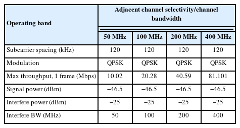
Adjacent channel selectivity test parameters
II. A Fourth Biquadratic Filter Design
The fourth-order LPF is shown in Fig. 2. It consists of two biquadratic filters and a complementary, structured source follower (SF). Because the active R-C filter is sensitive to low load impedance, the SF drives at the final stage for interfacing external instruments. If low load impedance is connected in the next stage without SF, the quality factor (Q-factor) of LPF is degraded by low load impedance.

Overall block diagram.
1. Biquadratic Filter
In LPF design, if the GBW of OPAMP is the same as or larger than the LPF’s 3 dB frequency, the changes in the characteristics of the LPF by OPAMP can be ignored. At the same time, in wideband LPF, because the pole of OPAMP may not cover the LPF’s 3 dB frequency, exact calculation with non-ideal OPAMP should be considered. Figs. 3 and 4 show the biquadratic filter circuit with OPAMP and a system block diagram. The filter is equal to a feedback circuit with 1/Q and unit gain feedback paths and two integrators. The transfer function of the block diagram is expressed in Eq. (1). In Fig. 4, because OPAMP should operate as an integrator to be the same as the ideal transfer function, OPAMP performance is crucial. In the conventional integrator, which is shown in Fig. 5, OPAMP is not ideal, and its transfer functions should be calculated to equal the ideal transfer function. Eq. (2) shows the calculations of the integrator transfer function with a single pole OPAMP system. This means that if the pole of the OPAMP system is the same as the integrator’s 3 dB frequency, and gain is sufficient for a feedback loop, the integrator transfer function can neglect the OPAMP's non-ideality. Fig. 6 shows the calculation of the transfer function with a non-ideal OPAMP. It should be assumed that the required minimum gain in an open loop system to obtain a closed loop gain is 40 dB, and OPAMP variables of 3 dB frequency make the filter transfer function change. To be the same as the ideal transfer function, the figure shows that the OPAMP's frequency should be at least 0.1 times the filter transfer function. Fig. 7 represents each Q-factor of the biquadratic filter. The proposed filter follows the response of the worth filter.

Biquadratic filter with non-ideal OPAMP.

Biquadratic filter's system block diagram.

Conventional integrator.
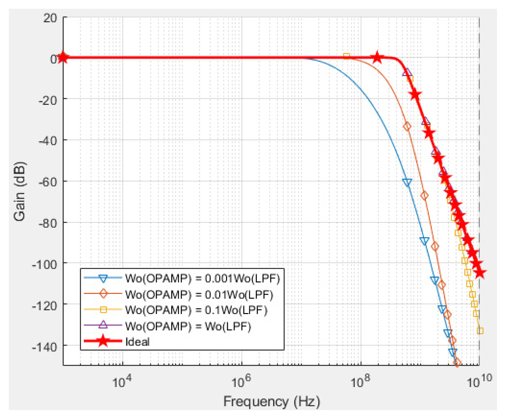
Transfer function with non-ideal OPAMP of 3 dB frequency variation (Ao,amp = 40 dB).
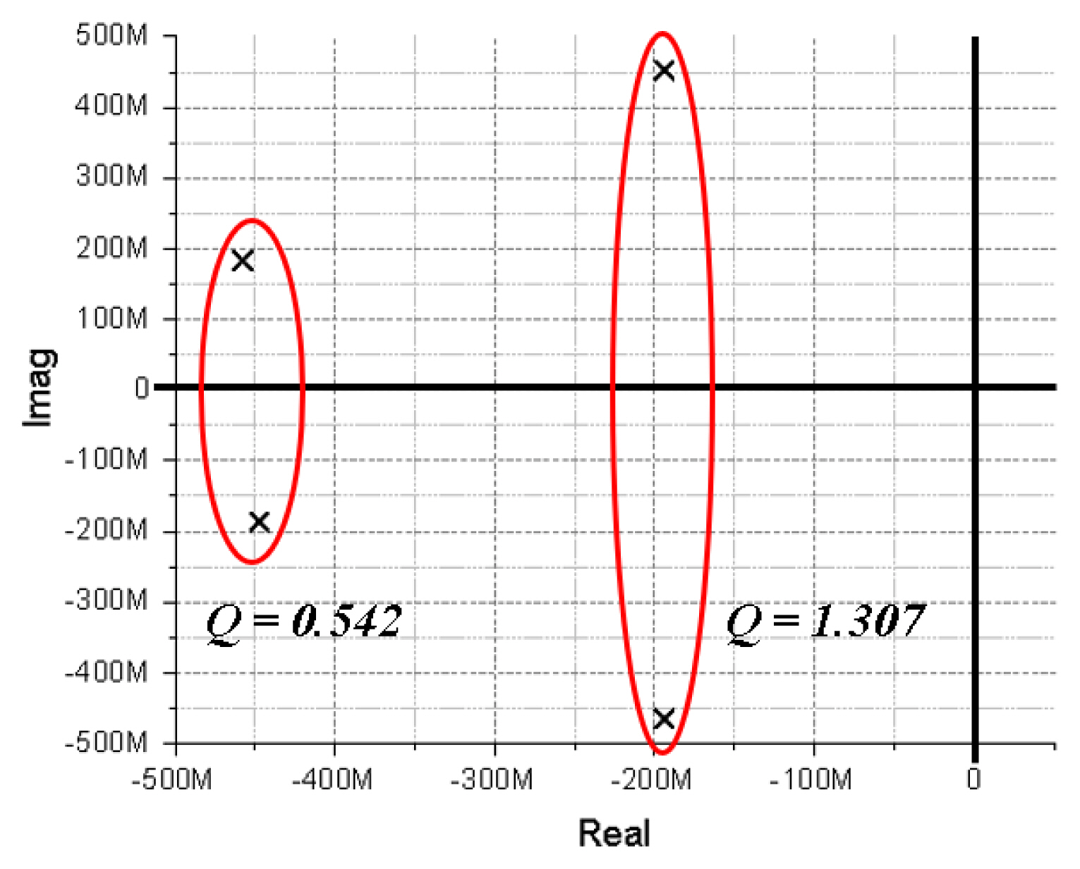
The fourth order filter transfer function pole and zero plot.
2. Wide Unit Gain Frequency OPAMP
This brief section will describe the proposed OPAMP, which was designed in two stages. Fig. 8 represents the proposed OPAMP. In the receiver baseband part, the roles of the variable gain amplifier (VGA) and LPF are amplifying the down-converted signals and filtering unwanted signals [3]. Thus, the linearity of the baseband is crucial. This means that the LPF should drive large input and output signals without gain compression. However, an NMOS single input cannot drive a signal near the ground, and PMOS cannot drive near the supply. This means the single MOS type of OPAMP suffers gain compression from the triode region near the supply or ground. Meanwhile, a complementary structure ensures the operation of saturation mode within a wider input/output range than the single MOS type. The complementary structure has nearly twice the transconductance of the single MOS type, with the added advantage of a larger GBW. For understanding the complementary structure, compare with previous studies [4–8]. As a result, complementary is appropriate when designing an LPF. The proposed OPAMP consists of the main signal part and the common mode feedback (CMFB) part, the structures of which are complementary. The main signal part is divided into two stages and the CMFB part is in three stages.
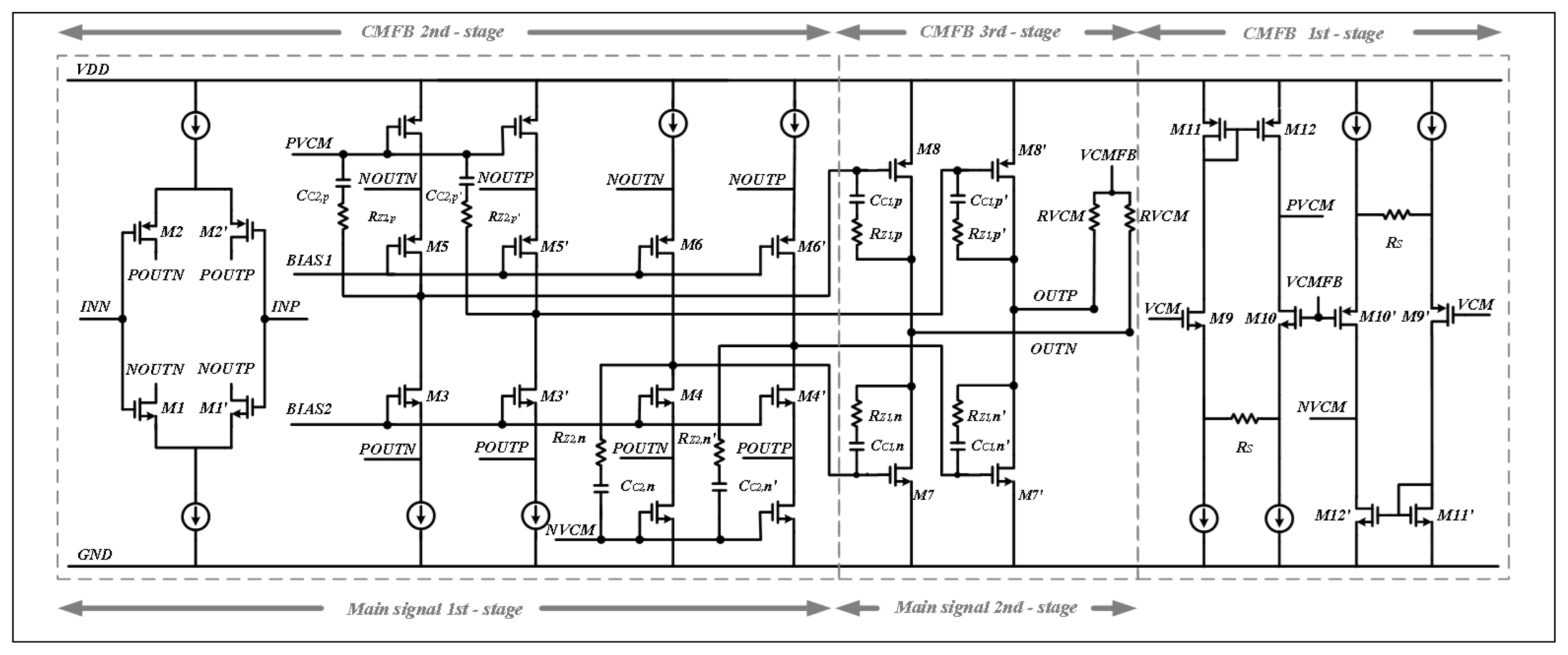
OPAMP overall schematic.
2.1. Main signal part
The main signal part is shown in Fig. 8. The main signal part has a PMOS and NMOS complementary structure. This structure can achieve larger transconductance, because the PMOS and NMOS of the input stage operates simultaneously. The proposed OPAMP consists of two complementary two stages, which are the folded cascode stage and common source stage. For stability, the OPAMP should be designed with a single pole system. Because of the two stages, as the result, the Miller compensation technique is used [9]. The folded cascode stage has two poles, and the common source stage has one pole. However, because one pole of the folded cascode is usually out of the GBW, only one Miller compensation is needed in the circuit. As a result, the transfer function and pole-zero calculation in the main signal part are calculated as shown in Eq. (3). If satisfying the condition in Eq. (4), the transfer function is approximately a single pole system.
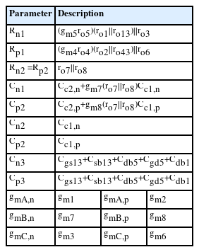
Fig. 9 shows the main signal part's small-signal equivalent circuits. The output of the first folded cascode stage is cascaded with the NMOS and PMOS inputs of the second common source stage. The exact pole-zero calculation is represented in Eqs. (5)–(6), where Rn1, Rp1, Rn2, Rp2, and Cn1 to Cn3 and Cp1 to Cp3 represent the resistances and capacitances of each stage, and gmA,n to gmC,n and gmA,p to gmC,p refer to transconductance, respectively as shown in Table 3.
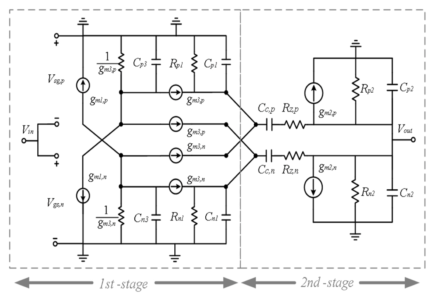
Main signal part small signal equivalent circuit.
OPAMP signal loop parameter
Each pole and zero approximation of the NMOS-path and PMOS-path is shown in Eqs. (7)–(8). The dominant pole of each path is the node of the middle of the first and second stages. Because of second stage gain, which is boosted by Miller capacitance in signal loop and Miller capacitance in CMFB loop, as well as LHP zero and pole cancellation, the second pole could be abbreviated without any effect. The third pole, which is larger than the GBW, is neglected. The total gain of OPAMP is the sum of the NMOS and PMOS pair, as shown in Eq. (9).
The total transfer function is shown in Eq. (10):
2.2. Common Mode Feedback Part
Regarding the LPF, the circuit is usually designed as a kind of feedback circuit that consists of a passive component and OPAMP. However, the feedback path does not contribute to the stability of the output node’s DC level. The instability of the output node DC’s level causes performance degradation. To prevent its saturation, a CMFB circuit should be considered to determine DC level in the OPAMP. The CMFB part is shown in Fig. 8. It consists of three stages: a current mirror load OTA, telescopic cascode, and common source stage. The main CMFB part is necessary to determine the output’s common mode voltage. Thus, a low main dominant pole frequency does not cause any issues in the circuit. Because the three stages and two Miller compensations are used, there is a trade-off point between high DC gain and low dominant pole frequency.
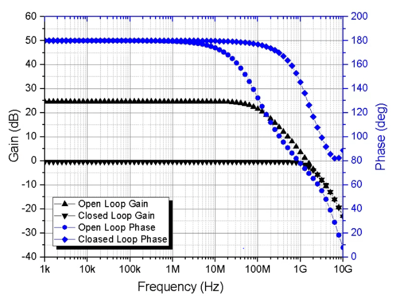
Fig. 10 represents the small-signal equivalent circuit of the CMFB part, which is a complementary structure with the NMOS and PMOS pairs. Between each stage, Miller compensation is used. The CMFB loop should be a single pole system like the signal path, as shown in Eq. (11). At this point, the second zero is right-half-plane (RHP) zero, which decreases the phase by 90°. Thus, the third pole and second zero should be 10 times larger than the GBW frequency, as shown in Eq. (12).
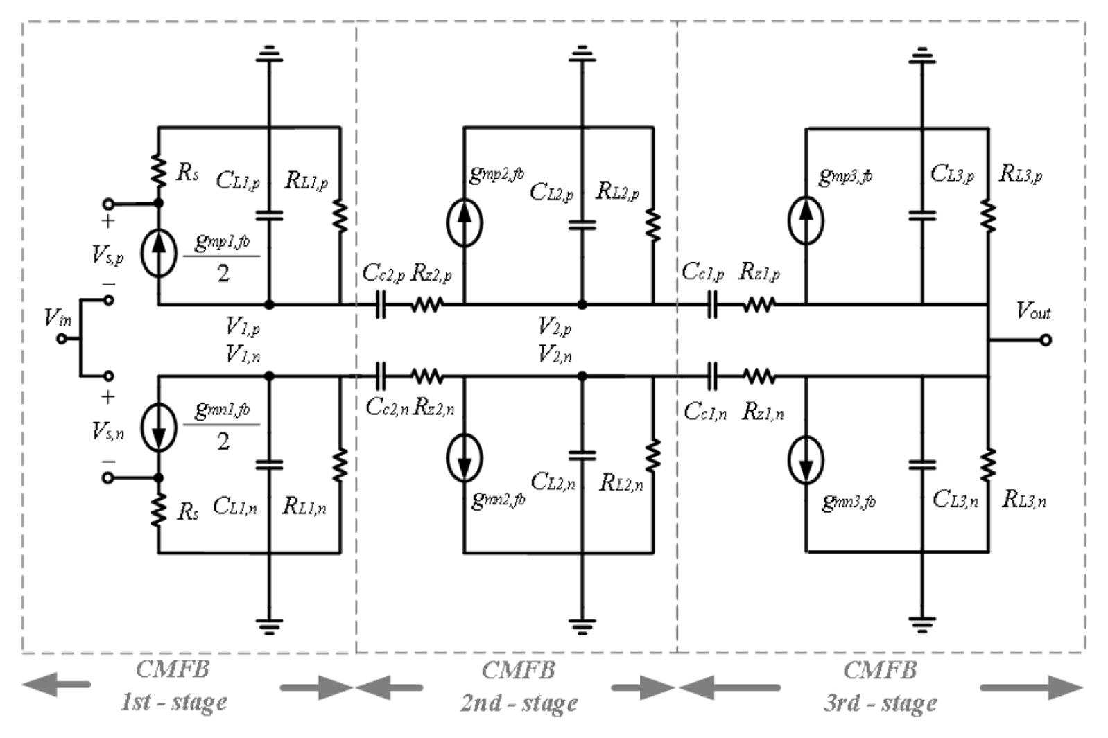
CMFB part small signal equivalent circuit.
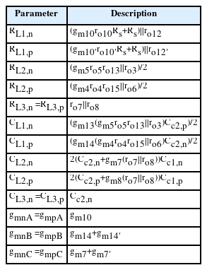
The exact pole-zero calculation is represented in Eqs. (13)–(14), where RL1,n to RL3,n and RL1,p to RL3,p and CL1,n to CL3,n and CL1,p to CL3,p represent the resistances and capacitances of each stage, and gmnA to gmnC, and gmpA to gmpC indicate transconductance, respectively, and are shown in Table 4. The CMFB part is the same as the main signal part with the NMOS and PMOS pair, as shown in Eqs. (15)–(16). The total gain is the sum of the NMOS and PMOS pair, as shown in Eq. (17).
OPAMP CMFB loop parameter
Table 5 is the OPAMP simulation results. The OPAMP open-loop gain is 59.9 dB and its phase margin is 65°. Fig. 11 shows that the OPAMP is designed as a single pole system within the GBW. Fig. 12 shows the CMFB loop stability. Because of the second zero and third pole, the phase decreases rapidly in the band over GBW. Both phase margins cover 60°, with any value over that meaning the circuit is stable. The complementary structure and common source of the second stage take advantage of large the input/output signal. Fig. 13 shows good linearity, in that OP1dB is 4.9 dBm.

Simulation results of OPAMP
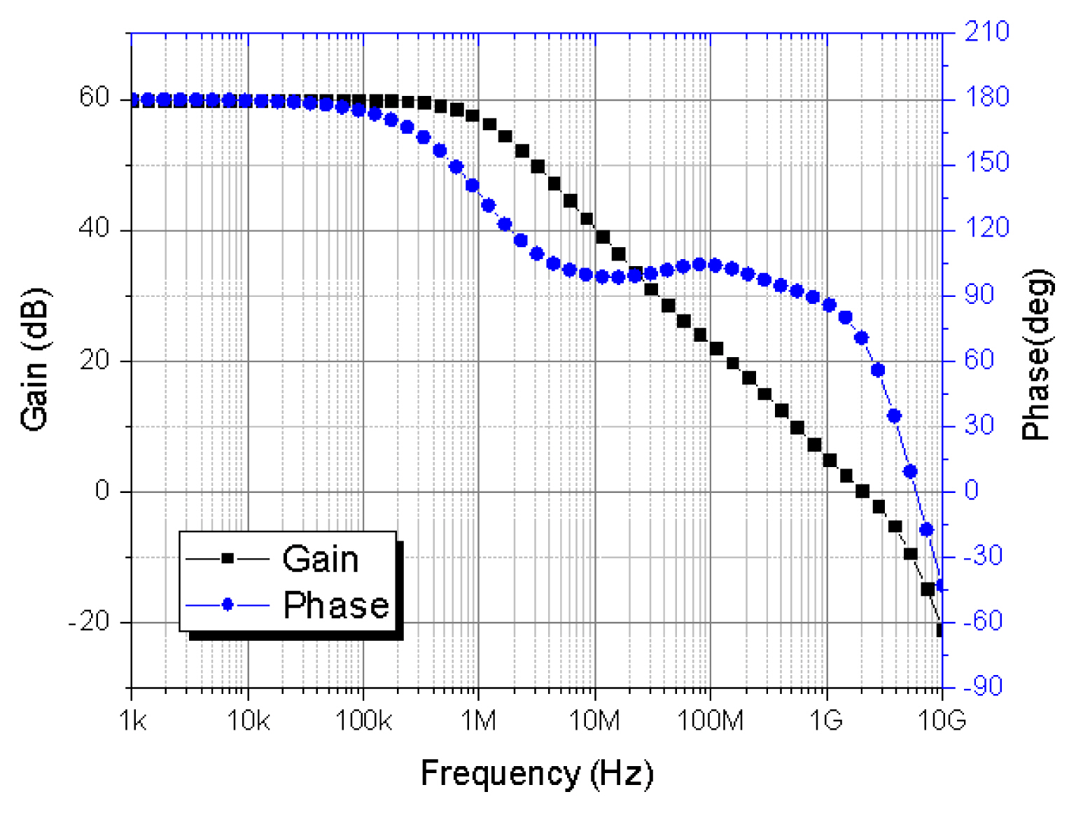
Proposed OPAMP transfer function.

CMFB loop stability.

OPAMP linearity.
3. Source Follower
The source follower is described in Fig. 14. The structure consists of two cascaded amplifiers, which are the current mirror load OTA (operational transconductance amplifier) and the common source with the diode connected load. Because of the diode-connected-load at the output node, the circuit is subject to low output impedance. The feedback path of 1 with feedback factor β makes the 3 dB frequency the same is the unit gain frequency; the output node of the OTA is the dominant pole. This is like a unit gain buffer with low output impedance. The SF also consists of a complementary structure. The P-type and N-type SF operate in other saturation regions (Fig. 15). The SF open-loop transfer function is shown Eq. (18).

Source follower schematic: (a) PMOS source follower and (b) NMOS source follower.
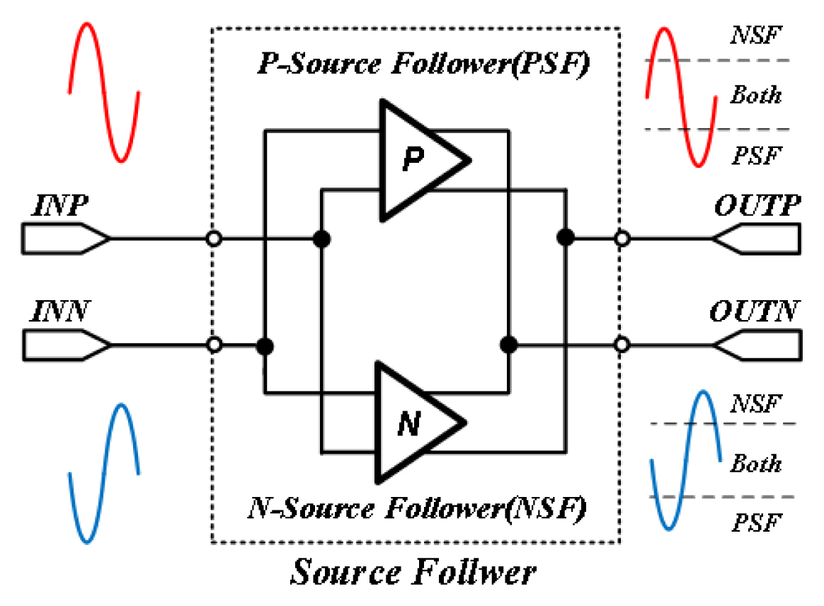
Complementary source follower block diagram.
where sωVp1 is the first pole at node V1.
Figs. 16 and 17 show the transfer functions (including that of the DC). The exact description of the SF has been explained elsewhere [10]. Table 6 presents the SF’s simulation results. Low output impedance driving causes two features. First, the output node pole is in the high frequency band. As a result, the SF has only single pole system in an operating frequency band. Second, the output node requires a 50 Ω driving current. The output's common mode voltage should maintain VDD/2 with 50 Ω load impedance. As a result, a large DC current is needed in circuit.
Simulated source follower transfer function.

Simulated source follower DC transfer function.

Simulation results of source follower
III. Simulation and Experiment Results
The filter is fabricated in a CMOS 65 nm process. The chip of the area is 0.18 mm2, as shown in Fig. 18(a). The measurements are implemented as follows:

(a) Die photo and (b) test environment for measurement.
- The designed filter is set by wire bonding on printed circuit board (PCB),as shown in Fig. 18(b).
- The differential input signal is made by a balun, which makes single to differential signal, this covers 6.5 MHz to 4 GHz.
- Input and output impedance are matched at 50 Ω by the R and, C elements on the PCB. The output node is connected to the spectrum analyzer (E4440A) and oscilloscope.
- Passed signal after balun is nominated input signal.
With the CMFB circuit, not only could the output DC of the two-stage differential OPAMP block unwanted noises from the supply or ground, but the output voltage will also follow a reference voltage, as shown in Fig. 19. The measured 3-dB frequency is 330–630 MHz. Compared with the simulated 3-dB frequency, there is a small difference (simulated result 384–681 MHz). The 3-dB frequency is tuned by tunable capacitor C (C=C1=C2, in Fig. 3) The simulated and measured transfer function is shown in Fig. 20. In the in-band area, the ripple is 2.5 dB. The filter 3-dB cutoff frequency does not seem to be degraded by the SF, because the SF's GBW which is 1.09 GHz, covers the filter’s transfer function. The linearity measurement is implemented at the main tone of 100 MHz and another tone of 110 MHz. The two-tone test measurement is shown in Fig. 21. The simulated OIP3 is 11.7 dBm, and the OP1dB is 0.7 dBm (differential zero to peak value). The measured OIP3 is 8.45 dBm and OP1dB is −1.3 dBm. The measured differences from simulation are 3.25 dB in OIP3 and 2 dB in OP1dB, because there are losses when implementing the mask layout and measurement environment.
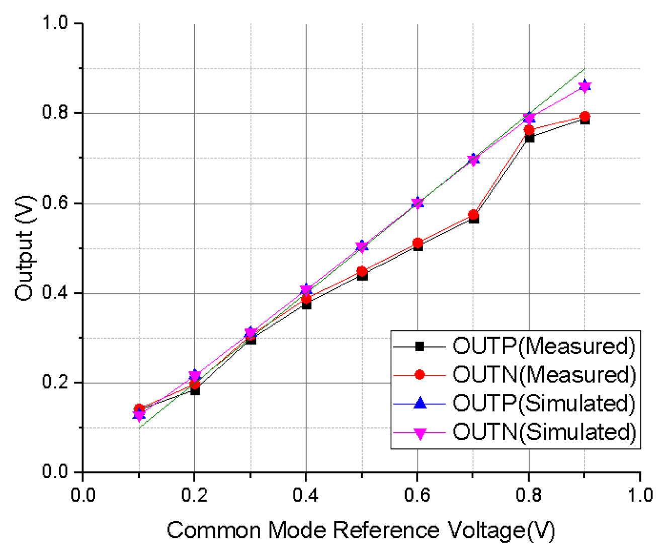
Reference voltage vs output DC voltage.
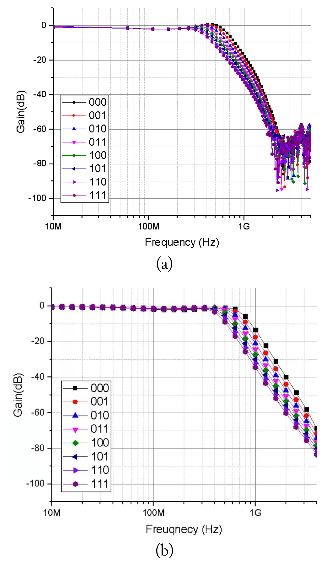
(a) Measured LPF transfer function and (b) simulated LPF transfer function.
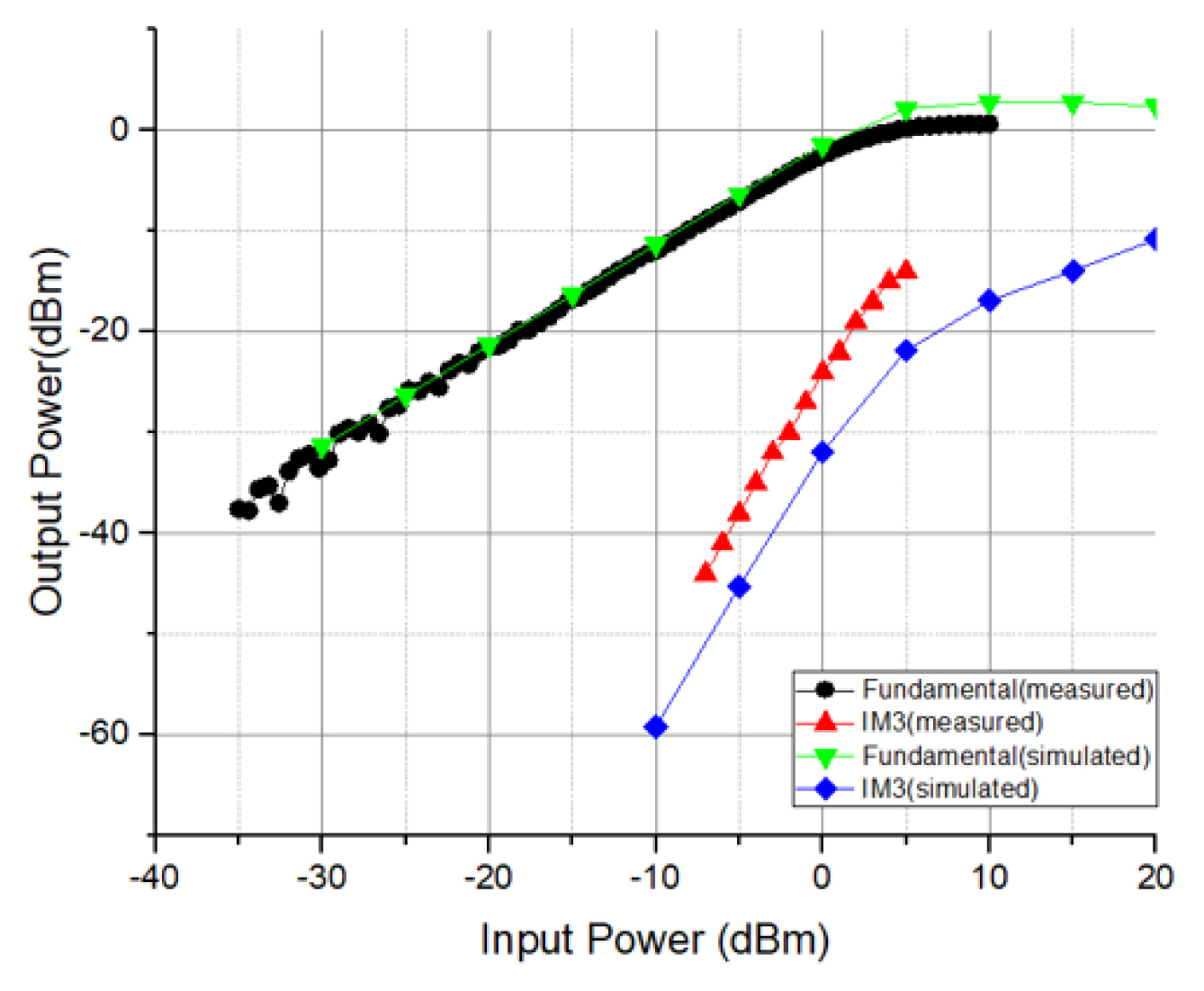
Linearity of the LPF.
Fig. 22 shows the output noise of the filter. Because the gain is 0 dB, the input referred noise (IRN) could be equal to the output noise, Fig. 23 shows the total harmonic distortion (THD); after the −10 dBm input signal at 50 MHz passes the LPF, the measured THD is −44.6 dB. Table 7 compares the specifications of this work with those of recently published papers [11–13].
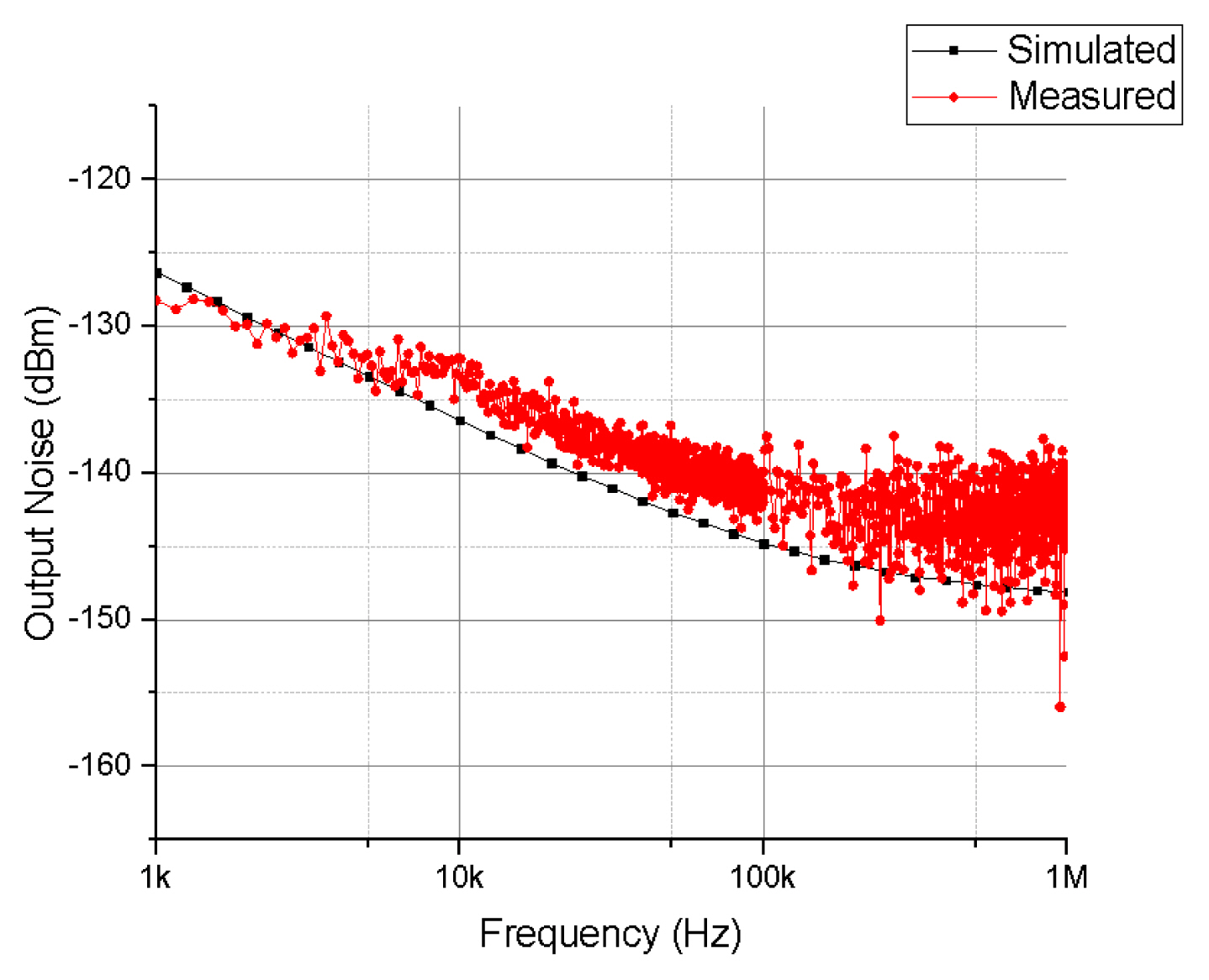
Output noise of the LPF.

THD measurement of the LPF.
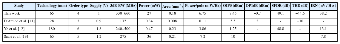
Summary of this work with recent other works
IV. Conclusion
As a wideband LPF for the new 5G standard needs to be designed, this paper presents a wideband active R-C LPF with large GBW and complementary structured OPAMP in a 65 nm CMOS process. In the active R-C filter design, the performance of OPAMP is the most crucial point. The GBW of the OPAMP should be much larger than the 3-dB frequency of the LPF. In this system, there is a trade-off between bandwidth and current consumption. Because of the complementary two-stage structure, the proposed filter has a larger input/output signal range. Also, because the sensitive output impedance of the LPF should be isolated from low output impedance, an SF circuit needs to be inserted into the circuit. However, because the SF drives 100 Ω impedance without degrading linearity, the current consumption of the SF is nearly 11 mA. If there is a condition to drive large impedance in some applications, the current of the SF can be significantly reduced. Without the SF, the filter current consumption is 16 mA. Another advantage of the proposed filter is a wide variable range from 330 MHz to 660 MHz with a low THD of −44.6 dB. Compare with recent papers, the proposed circuit operates at low supply voltage and wide bandwidth.
Acknowledgments
This work was supported by a Korea Institute for Advancement of Technology (KIAT) grant funded by the Korea government (MOTIE) (No. P0017124, The Competency Development Program for Industry Specialists), and the K-Sensor Development Program (No. RS-2022-00154729) funded by the Ministry of Trade, Industry, and Energy (MOTIE, Korea).
References
Biography

Chang-Kyun Noh obtained his B.S and M.S. degrees from the Department of Electrical Engineering, Korea Aerospace University, Goyang, Korea in 2022. His research interests include the design of RFIC and radar systems.

Hyun-Yeop Lee received his B.S. degrees from the Department of Electrical Engineering, Korea Aerospace University, Goyang, Korea in 2021. His research interests include the design of RFIC, data converters, and radar systems.

Ho-Jin Kang obtained his B.S and M.S. degrees from the Department of Electrical Engineering, Korea Aerospace University, Goyang, Korea in 2022. His research interests include the design of RFIC and radar systems.

Sung-Tae Kim received his B.S. degrees from the Department of Electrical Engineering, Korea Aerospace University, Goyang, Korea, in 2021. His research interests include the design of RFIC and radar systems.

Ho-Seon Baek received his B.S. degrees from the Department of Electrical Engineering, Korea Aerospace University, Goyang, Korea in 2021. His research interests include the design of RFIC and radar systems.

Young-Jin Kim received his B.S. degree in electrical engineering from Kyungpook National University in 1995. He received M.S. and Ph.D. degrees in electrical engineering from the Korea Advanced Institute of Science and Technology (KAIST) in 1997 and 2002, respectively. His Ph.D. dissertation focused on the transceiver architecture of image rejection and spurious rejection. In 2002, he joined Samsung Electronics Co. Ltd., Korea, as a Senior Engineer. Since then, he has participated in the design of CDMA and GSM/GPRS wireless mobile applications. Furthermore, he has designed an LNA and down-conversion mixer for multimode CDMA and GSM/GPRS. In 2006, he joined the School of Electronics and Information Engineering, Korea Aerospace University, Goyang, Korea.