


I. Introduction
Terahertz (THz) technology has been proposed as a new inspection tool in various fields [1, 2]. Particularly, for medicine, foods, security screening, and nondestructive testing, a new inspection method is required due to the limitations of the existing inspection technology [3ŌĆō7]. The transmission and absorption of THz waves for various materials, a high sensitivity to moisture, and low ionization energy are key to applying THz technology in these fields. Recently, the development of various high-power THz sources and high-sensitivity detectors has led to the expansion of THz technology into industrial applications.
For industrial applications of THz waves, THz imaging technology using compact continuous-wave (CW) high-power THz sources and high-sensitivity detectors is expected to be applied in many industrial fields requiring nondestructive, non-contact, and noninvasive methods [8, 9]. However, as the frequency increases, a dramatic decrease in the output of the THz source and a low detection sensitivity are obstacles to applying THz. For this reason, a THz source and a detector in the low-frequency region are preferred in many applications. A THz source in the low-frequency region has a high output power, so it has advantages in inspecting a thick sample or in scanning a large area. However, the low spatial resolution and diffraction due to the inherent wavelength make it difficult to apply the THz wave to an industrial field that requires a high resolution.
Recently, numerous studies on improving spatial resolution have been conducted [10, 11]. A resonant slit-type probe for the THz frequency range, which has a simple structure, high coupling efficiency, and linear polarization, has been proposed, and one with a slit height less than 1/10 of the wavelength and a slit width of approximately half the wavelength can easily achieve high spatial resolution [12, 13]. This is useful in applications where small defects or enclosed foreign objects must be detected.
In this study, THz technology was applied to industrial applications that require safe and high-resolution detection. For the latter, a resonant slit probe operated at 200 GHz was designed and manufactured, and it was applied to the inspection of voids in a multistack semiconductor, which is an issue in the semiconductor field. In addition, it was applied to the inspection of foreign objects that are frequently mixed in the tablet manufacturing process in the pharmaceutical field.
II. Resonant Slit-type Probe with A Rounded Matching Structure
According to BabinetŌĆÖs principle, the impedance (Zs) of a slit antenna is
where ╬╗0 is the free-space wavelength and w and h are the width and height of the slit antenna, respectively [14].
Assume that a narrow slit is attached to the end of a waveguide. The maximum transmission occurs when the waveguide impedance and slit impedance match. If the width and height of the waveguide are a and b and the width and height of the slit are aŌĆ▓ and bŌĆ▓, then from Eq. (1),
and
In other words, the slit becomes transparent under the above conditions [15]. In Eq. (3), if bŌĆ▓ approaches 0 (zero), then this equation is satisfied at ╬╗=2a. This means that if the width of the slit is half the wavelength, then the height of the slit can be infinitely reduced. That is, electromagnetic waves of a specific frequency according to the above conditions can pass without loss through a very narrow slit.
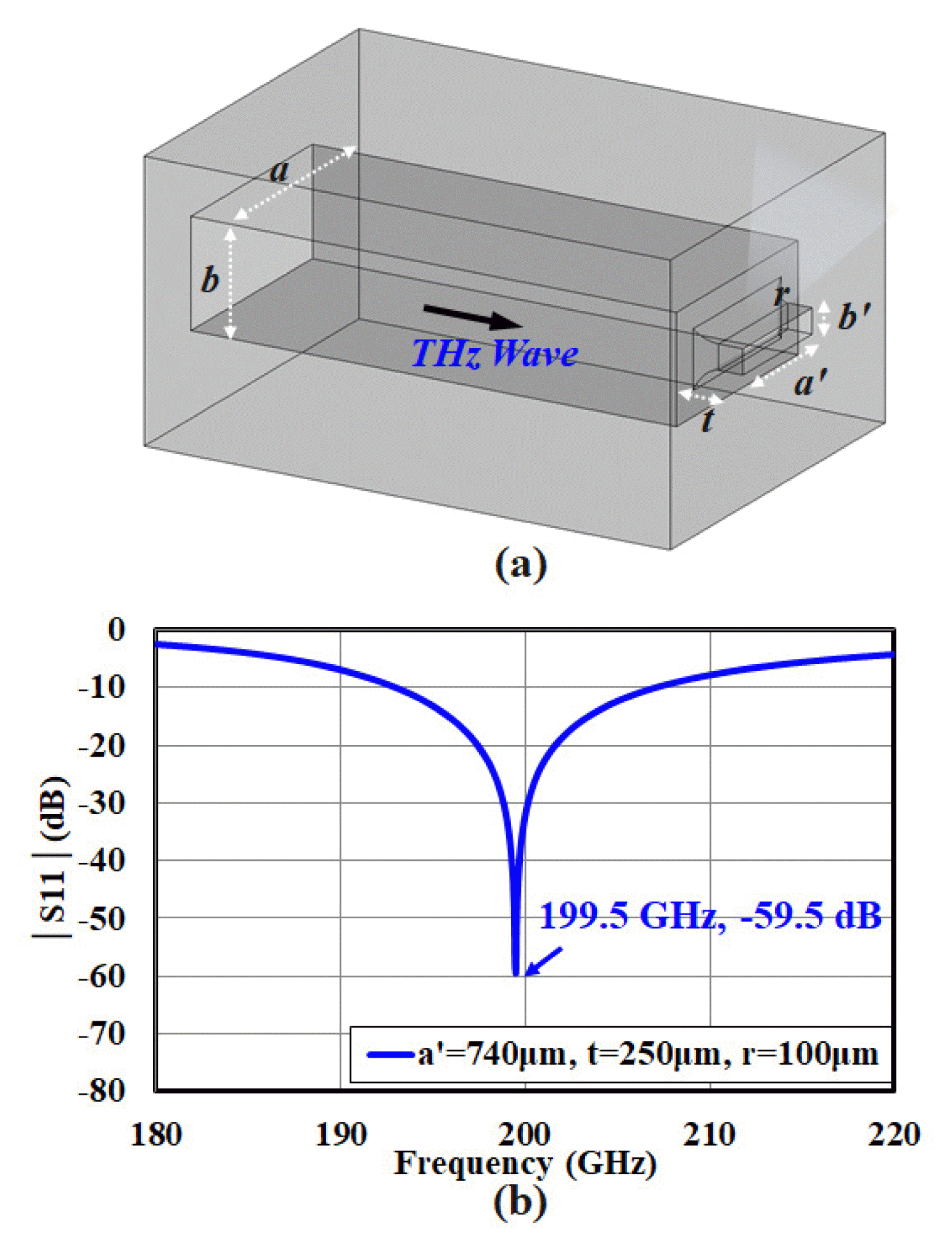
Figure 1(a) shows a schematic diagram of a resonant slit probe with a rounded matching structure for impedance matching. The proposed structure is optimized to have a resonant frequency at 200 GHz using CST simulation. The designed slit structure has a slit width of 740 ╬╝m (~╬╗/2) and a slit thickness of 250 ╬╝m, and the radius of the matching structure is 100 ╬╝m. The slit height is fixed at 150 ╬╝m (=╬╗/10). Fig. 1(b) shows the frequency response characteristics of the designed resonant slit probe. The resonant frequency is 199.5 GHz, and the return loss at the resonant frequency is calculated as 59.5 dB.
III. Void Inspection in A Multistack Semiconductor using the Resonant Slit Probe
In recent years, such devices as mobile phones and laptops have been expected to offer high-speed processing technology while exhibiting compact and lightweight characteristics. To solve this problem, in recent semiconductor technology, multistack semiconductors, in which chips are multistacked by a chip packaging method, have been widely used. In the stacking method, die attach film (DAF) is commonly used. The bonding method using DAF has the advantage of the easy application of a certain amount and a simple bonding process [16, 17]. However, a problem arises due to voids occurring between the film and the chip in the bonding process. Internal voids larger than a certain size expand when the temperature of the device rises, causing cracks in the chips. Therefore, it is important to be able to detect voids in a multistack semiconductor in the chip packaging process.
The ultrasonic inspection method has been used to inspect voids in multistack semiconductors [18,19]. However, in underwater ultrasonic inspection, the semiconductor cannot be used after inspection due to the invasiveness issue. In addition, infrared (IR) inspection [20] cannot be used due to the high absorption rate of DAF polymer materials, and X-rays cannot be applied due to ionization of semiconductor materials under high X-ray energy. The THz wave is the most ideal light source for semiconductor inspection because it has high transmittance through silicon and polymers, which are semiconductor materials, and it does not ionize semiconductor materials with low photon energy.
Figure 2 shows a photograph of the void inspection system for a multistack semiconductor using the resonant THz slit probe. The complex metal pattern on the top of the semiconductor chip makes it difficult to transmit the THz wave through the chip. In contrast, polypropylene (PP) is mainly used as a DAF material for semiconductor lamination, so THz waves can easily pass through the films because PP has a small absorption coefficient of less than 5 cmŌłÆ1 in the THz region. Therefore, we built an inspection system using the lateral scan method on the side of the multistack semiconductor. In addition, the slit probe was applied to the front end of the detector to identify the positions of the voids in the multistack semiconductor.
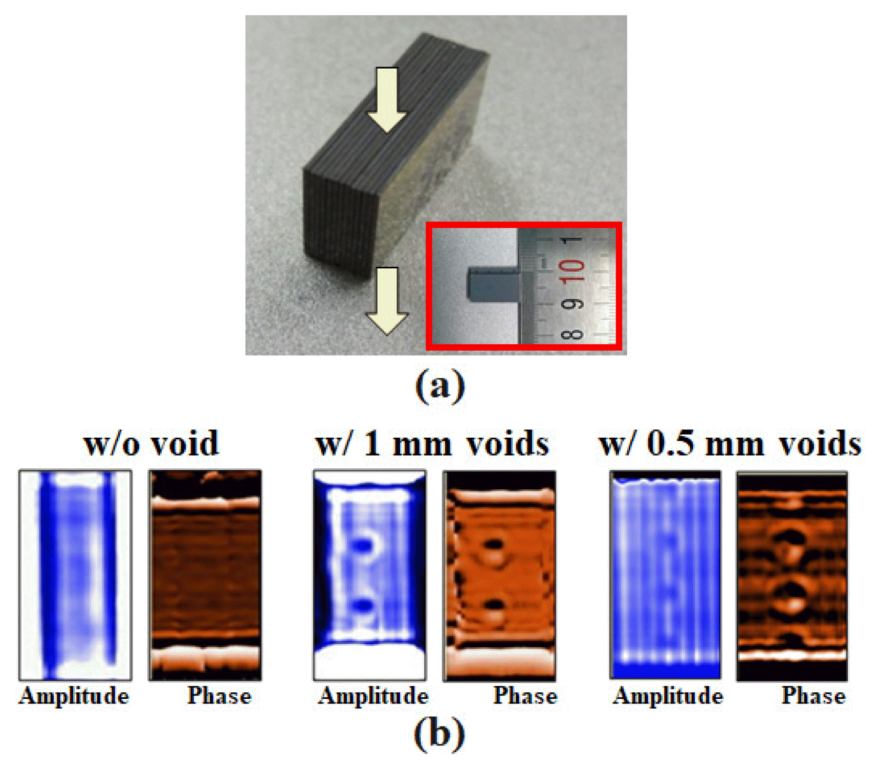
A photograph of a multistack semiconductor package is shown in Fig. 3(a). The number of stacked chips is 13, and the chip thickness in the transmission direction is 8.6 mm. Chips with void diameters of 1 mm and 0.5 mm were fabricated and placed in stacked semiconductors. Fig. 3(b) shows THz images of the amplitude and phase of the measured signal for a package sample without voids and package samples with 1 mm and 0.5 mm voids.
As shown in the figure, even though a light source of 200 GHz (╬╗=1.5 mm) was used, even voids with a diameter of 0.5 mm, smaller than the wavelength, were detected. Particularly, small voids are easier to detect in the phase image than in the amplitude image because the attenuation of the amplitude at the small-diameter voids is small, but diffraction of the THz wave easily occurs in the voids due to the short wavelength. In addition, the positions of the voids could be distinguished because the height of the slit probe used was less than the height of the DAF. Because the signal range detected with the long slit length was measured to be wider than the void diameter, accurately determining the size of the voids was difficult. However, void inspection using THz waves was verified as a possible solution for detecting voids larger than a certain size.
IV. Inspection of Foreign Objects in A Tablet using the THz Probe
In the pharmaceutical field, X-ray inspection is mainly used for foreign body inspection, but it is avoided because of concerns about the harm caused by high energy. In addition, detecting foreign objects, such as rubber and plastics, is difficult because of the low detection sensitivity of X-rays for soft materials. The photon energy of THz waves is approximately one million times less than that of X-rays, making them an ideal light source for applications requiring safe inspection [21]. Recently, a laser-based THz inspection system was developed [22], but it has not been applied to manufacturing due to the limitation of the inspection speed.
To improve the detection speed, we applied high-speed lock-in amplifier technology using TTL modulation of a semiconductor-based CW THz source. The applied high-speed lock-in amplifier can perform signal processing even under the high-speed modulation of several tens of kHz, so it can detect signals with a high signal-to-noise ratio (SNR) even under high-speed scanning of several tens of cm/s.
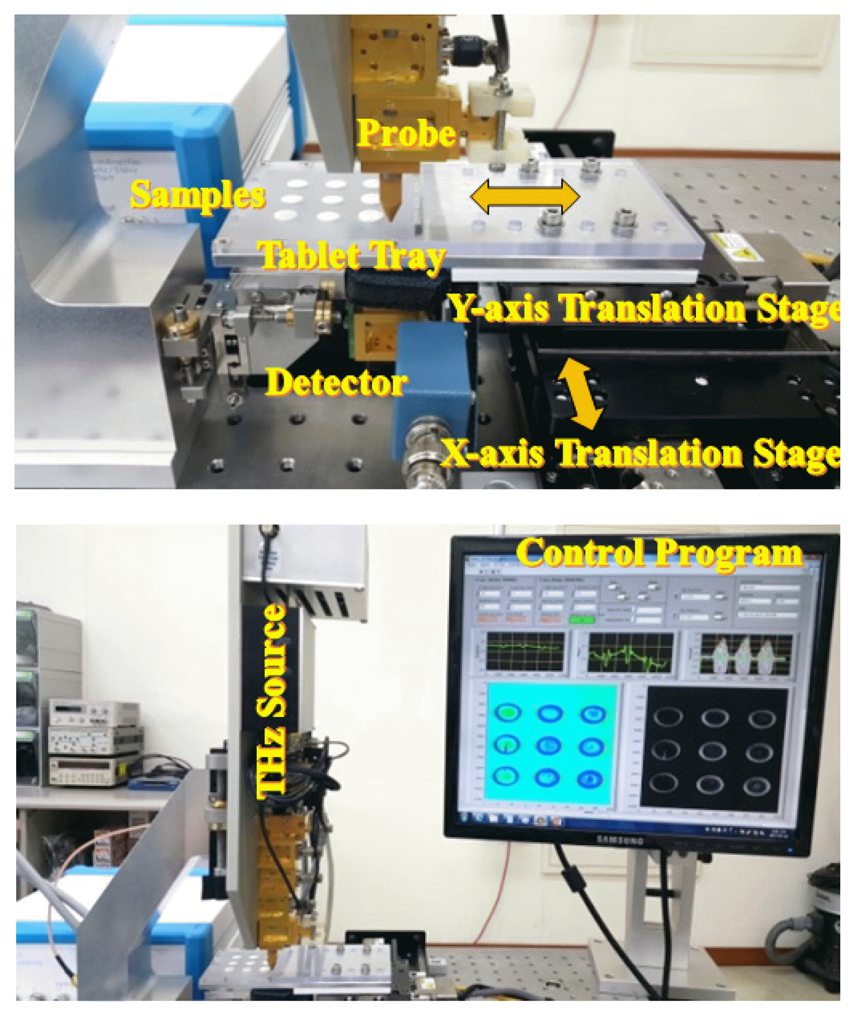
Figure 4 shows the THz system and control program for the inspection of foreign objects in tablets based on CW THz waves. The samples were placed in the holes of a tablet tray made of plastic. For 2D scanning, the tablet tray was fixed to an XY translation stage, and the source and detector were installed close to either side of the tablet tray. The THz signal transmitted through the tablets was displayed to identify foreign objects in the tablets.
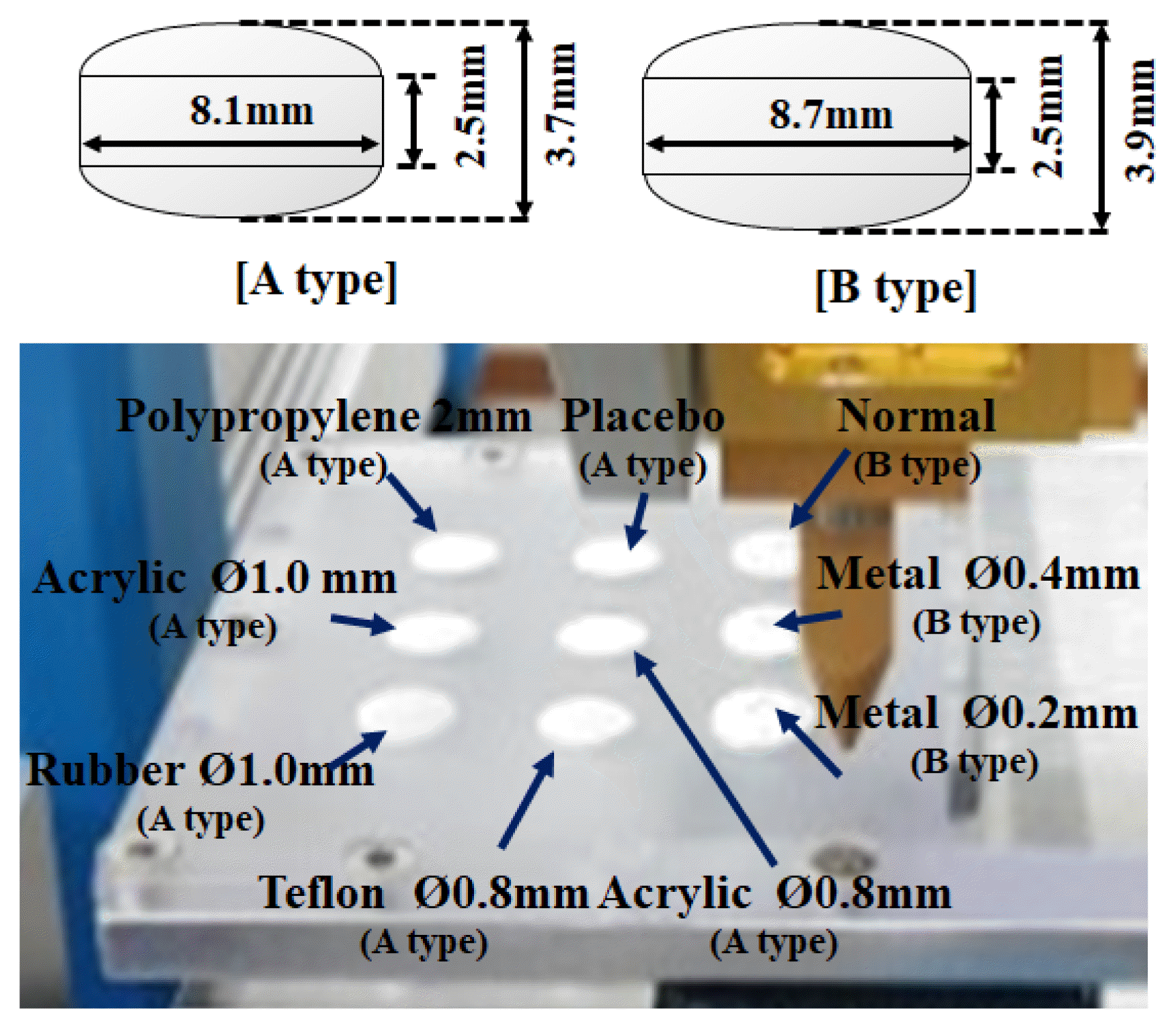
Structure diagrams of the tablet samples are shown in Fig. 5(a). The samples were of two types: a round tablet with a diameter of 8.1 mm and a height of 3.7 mm (A-type) and a round tablet with a diameter of 8.7 mm and a height of 3.9 mm (B-type). Considering the applications of THz inspection, the tablet structures commonly encountered in pharmacies were selected. For A-type tablets, a PP piece, an acrylic piece of 1.0 mm or 0.8 mm, a rubber piece of 1.0 mm, or a Teflon piece of 0.8 mm was included in the manufacturing process. The foreign object included in the B-type tablets was a small metal rod with a diameter of 0.4 mm or 0.2 mm.
Figure 6(a) shows the transmitted THz image for the samples in Fig. 5, and Fig. 6(b) shows the X-ray image for comparison. Comparing the THz image with the X-ray image, most foreign objects were detected in the THz image, whereas only metal rods, PP, and the Teflon piece were detected in the X-ray image. First, rubber was not detected in the X-ray image because of the low sensitivity of X-ray to soft materials. Second, although acrylic is a polymer, similar to PP and Teflon, it was not detected by X-ray inspection. An X-ray image is an image produced according to the attenuation coefficient. The attenuation coefficient of acrylic according to the X-ray energy is located between those of PP and Teflon [23]. From the X-ray image, the reason the acrylic object in the tablet was not detected in the X-ray image can be determined to be the similarities in the attenuation coefficients of the tablet and acrylic. In contrast, THz images contain various information, such as the dielectric constant, absorption rate, and diffraction and refraction of materials. In the measured THz image, the amplitude of the THz signal decreased in all the foreign object regions in the tablets because, as in many studies, diffraction occurs at small foreign objects in the path of THz waves.
V. Conclusion
In this study, the industrial applicability of THz inspection technology was verified. THz probe-based inspection technology was applied to the semiconductor and pharmaceutical inspection fields, which require safe, high-resolution inspection. In semiconductor inspection using THz waves, voids with a diameter of 500 ╬╝m were detected in stacked semiconductors. Moreover, by using the resonance-type slit probe, even the positions of the voids in the stacked structures were distinguished. In the tablet inspection, all foreign objects in the prepared tablet samples were detected. In contrast, some plastics and rubber, a soft foreign object, were not detected in the X-ray inspection, as a comparison. From the results, the THz inspection technique can be confirmed applicable as a new inspection tool in areas where X-ray inspection is avoided.