


I. Introduction
The rapid erosion of coastal areas leads to cracks in the located foundations of houses in coastal areas and the loss of the white sand beach area. Moreover, coastal erosion increases the risk of coastal accidents, leading to a decline in tourism, which significantly affects the local economy. Therefore, continuous monitoring of the different forms of local coastal erosion is important. One available monitoring system is the ocean current observation sensor system. However, it is expensive and difficult to set up because it needs to be installed and operated underwater. Another drawback is its difficult handling due to the frequent loss of sand caused by the movement of underwater sand produced by strong currents. This necessitates a wave-only monitoring system that detects and analyzes wave information. Such a system can detect valuable information about waves, such as wave height, wave direction, and wave period. To obtain precise wave characteristics, a wave monitoring radar system has been researched and developed [1, 2]. The frequency band of a commercially available wave monitoring radar is conventionally X-band, which makes processing real-time big data signals difficult. To solve the problem of real-time big data signal processing, the authors propose high-gain antennas for a wave monitoring radar system operated at relatively high-frequency bands, such as the Ku-band [3, 4]. These antennas provide high resolving power and high resolution. Considering these factors and requirements, slotted waveguide array antennas are the best candidates for a required radar system. The characteristics of slotted waveguide array antennas vary depending on the shape, size, and arrangement of the resonance slots. The larger the number of resonance slots, the larger the size of the slot openings, providing better characteristics.
This study proposes a technique for designing a high-gain slotted waveguide array antenna to obtain a wave monitoring radar system for real-time big data signal processing. A 1 × 26 slotted waveguide array antenna is developed and then extended to a 6 × 26 array antenna.
The proposed antenna is designed using a high-frequency structure simulator, which is a three-dimensional simulation program based on the finite element method. To improve the gain, a waveguide with a guided wavelength greater than that of a standard waveguide is developed. In addition, the broad and narrow walls of the WR-51 standard waveguide are recalculated to control the beamwidth of the elevation and to select an azimuth suitable for this radar system. The lengths of the designed broad and narrow walls of the waveguide are 11.33 mm and 5.67 mm, respectively. The target frequency bandwidth ranges from 17.25 GHz to 17.75 GHz, with a center frequency of 17.5 GHz. The parametric characteristics and design processes are presented in detail in Section II, and the production and measurement results of the proposed antenna are given in Section III.
II. Antenna Design
1. 1 × 26 Slotted Waveguide Array Antenna
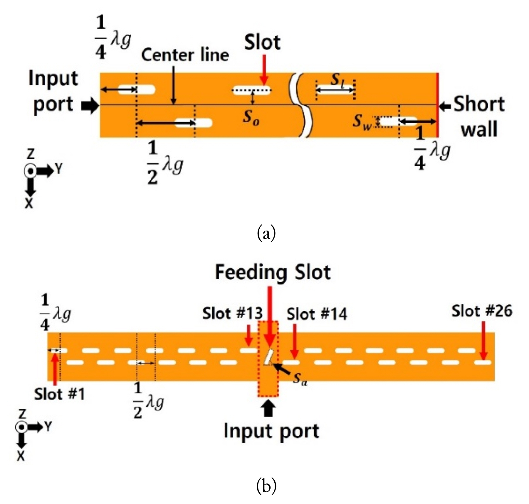
Fig. 1 illustrates the 1 × 26 slotted waveguide array antenna, highlighting the slots and the location of the feeding front. To investigate the change in the frequency band and gains with respect to the feeding position, the properties of the two antennas are compared by designing single-layer, as shown in Fig. 1(a), and double-layer structures, as shown in Fig. 1(b). In the single-layer structure, the feeding slot is designed to charge the plane waves at the location marked as the input port. The structure of the feeding slot is simple, but because it is located on the same layer as the feeding position, the complete planar feed-off is extremely difficult, leading to a large phase difference between slots [5]. Moreover, a strong current flows from the nearby slots to the feeding structure, restricting an even current distribution in all slots. Fig. 1(b) shows the double-layer antenna separating the feeding (lower layer) and radiating slots (upper layer). The feeding slot is placed as the lower layer at the center of the radiating slot array antenna. It is designed to charge a plane wave to the input port at the centralized feeding slot, allowing the current to be evenly distributed from the feeding slot to the resonance slots placed on both sides of the radiating slot [6, 7], thereby overcoming the drawbacks of the single-layer structure and achieving the required broadband characteristics by minimizing the change in imaginary impedance due to stacking. More benefits can be obtained across the broadband because of the symmetry of the radiating structure. The total electrical length of the single-layer antenna is 340.6 mm. As shown in Fig. 1, the distance between an input port and the first slot and between a short slot and the last slot are λg/4, respectively. The spacing between slots is equal to λg/2 to have the same phase [8]. The slot length (Sl) affects the resonance frequency; thus, iterative calculations are made to obtain the desired resonance frequency. Considering the slot width (Sw), the slot length is optimal in the range of λg/3 – 3λg/8. The width of the slot also affects the resonance frequency, but its contribution is lower than that of the slot length. To obtain the optimum resonant slot parameters through iterating calculations, the optimal width is in the range of λg/15 – λg/8 [9]. The slot offset (So) affects the real part of the impedance; thus, there is a small frequency shift. It is designed to have a greater effect on the reflection coefficient. The length, width, and offset of the resonance slots are accurately calculated. For the double-layer antenna, the total electrical length of the waveguide is 353.7 mm. The slots are placed as in the single-layer antenna. The size and slot angle (Sa) of the feeding slot are obtained using iterative calculations based on the reflection coefficients at a resonance frequency. The parameter values for the two antennas are listed in Table 1. The length and width of the feeding slot are designed to be the same as those of the resonance slot.
2. Analysis of the Reflection Coefficients
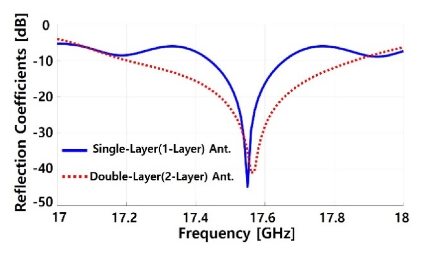
Fig. 2 shows a comparison of the reflection coefficients of the 1 × 26 slotted waveguide array antennas in Fig. 1 obtained through simulations. The solid blue line represents the reflection coefficients of the single-layer antenna. The simulated reflection coefficient is −30 dB at 17.5 GHz, and the bandwidth is 220 MHz when the reference level of the reflection coefficient is −10 dB. The red dotted line represents the reflection coefficients of the double-layer antenna. The reflection coefficient is −30 dB at 17.5 GHz, and the frequency bandwidth is 670 MHz when the reference level of the reflection coefficient is −10 dB. Therefore, the bandwidth of the double-layer antenna is wider than that of the single-layer antenna. The former satisfies the target bandwidth.
3. Analysis of Surface Current Distribution
Fig. 3 compares the surface current distribution of the 1 × 26 slotted waveguide array antennas in Fig. 1 simulated at a center frequency of 17.5 GHz. Fig. 3(a) and 3(b) show the surface current distribution of the single-layer and double-layer antennas, respectively. The surface current distribution is stronger for the double-layer antenna than for the single-layer antenna at 17.5 GHz. The result that the gain of the double-layer antenna is higher than that of the single-layer antenna is expected.
4. Analysis of the Radiation Patterns
Fig. 4 compares the radiation patterns of the 1 × 26 slotted waveguide array antennas in Fig. 1. The red solid line and the red dotted line represent the XZ-plane and the YZ-plane of the radiation pattern of the double-layer antenna, respectively. The solid blue line and the blue dotted line represent the XZ-plane and the YZ-plane of the radiation pattern of the single-layer antenna, respectively. The beam geometry of the radiation pattern of the antennas at each frequency is similar, and the resulting value of the antenna gain is higher for the double-layer antenna. This is due to the surface current distribution of the double-layer antenna being more concentrated than that of the single- layer antenna. Table 2 shows the peak gain of the antennas according to the radiation patterns shown in Fig. 4. The edge frequencies of the target bandwidth, 17.25 GHz and 17.75 GHz, exhibit higher gain characteristics for the double-layer antenna than the center frequency of 17.5 GHz.
5. Analysis of the Peak Gain
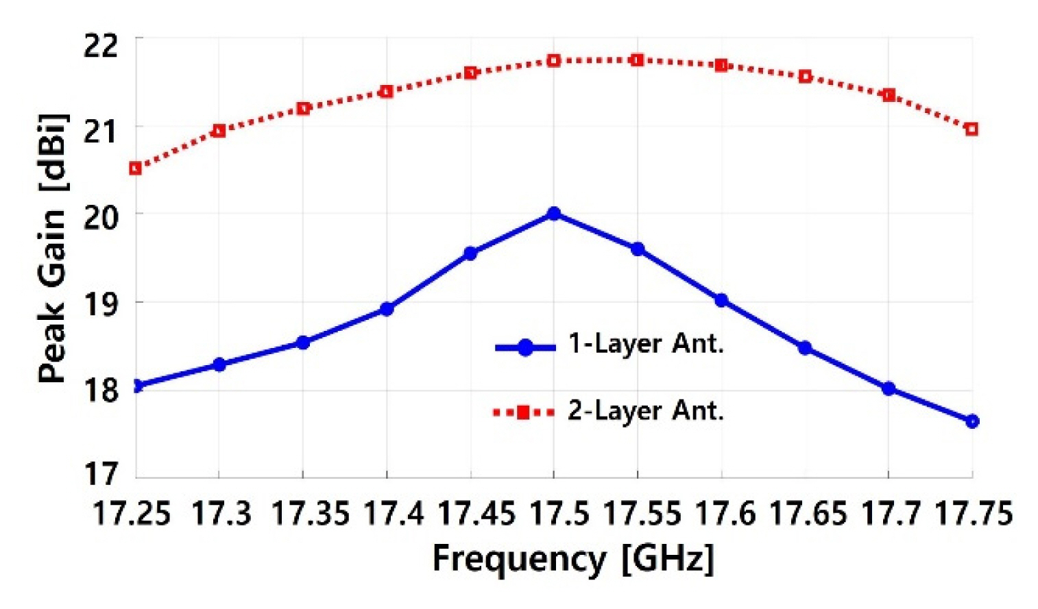
Fig. 5 shows a simulation comparison of the peak gains versus the frequency of the 1 × 26 slotted waveguide array antennas in Fig. 1. The blue solid line and the red dotted line represent the peak gain versus the frequency of the single-layer and double-layer antennas, respectively. Even though the simulated gains of the two antennas with different layers are calculated to be approximately above 20 dBi at a center frequency, the peak gain of the double-layer antenna is higher than that of the single-layer antenna in the target frequency band. As shown in Fig. 2, this is due to the frequency bandwidth of the double-layer antenna being broader than that of the single-layer antenna. Therefore, in this paper, the double-layer antenna is used because it has a better frequency bandwidth and gain to optimize the 6 × 26 slotted waveguide array antennas.
6. 6×26 Slotted Waveguide Array Antenna
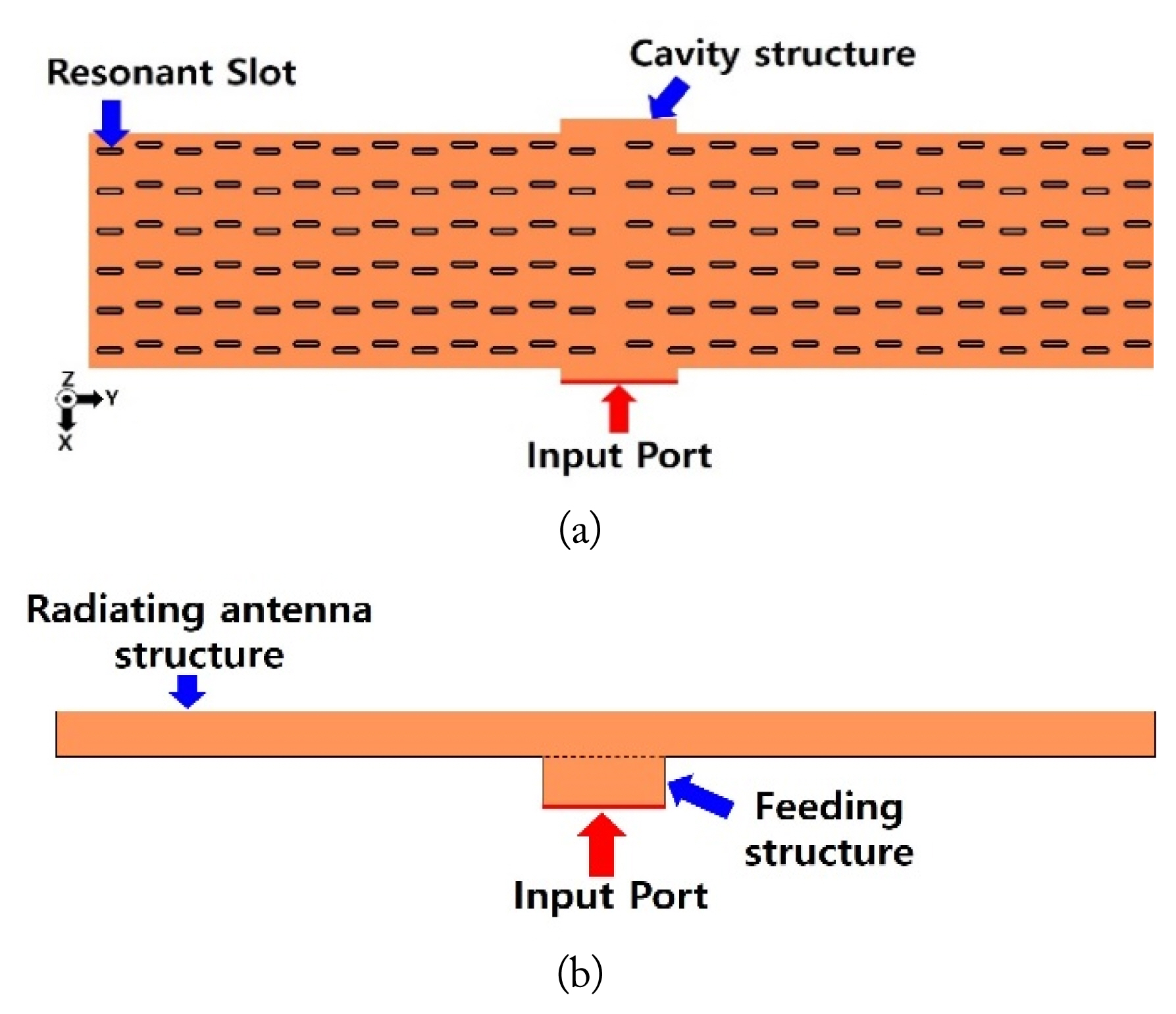
Fig. 6(a) illustrates the structure of the 6 × 26 slotted waveguide array antenna for the wave monitoring radar system that operates in the Ku-band frequency. Fig. 6(b) shows a side view of the combined feeding structure.
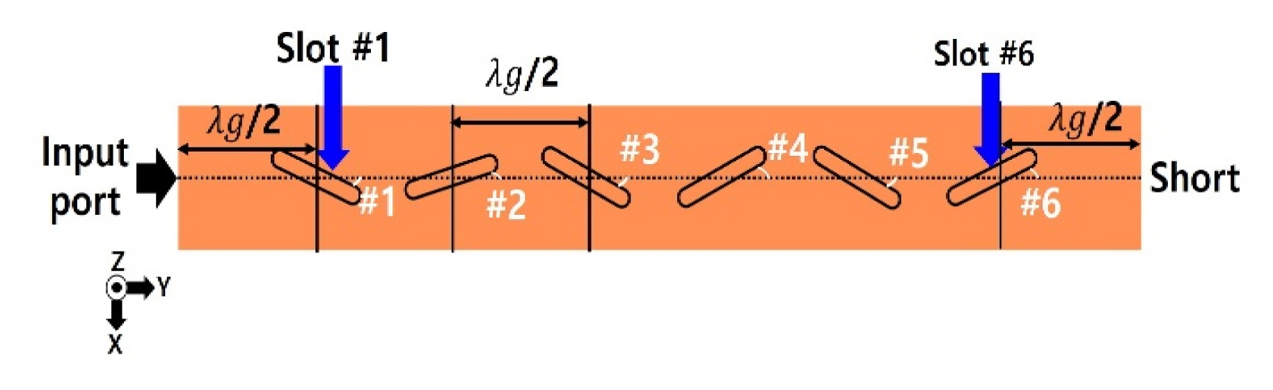
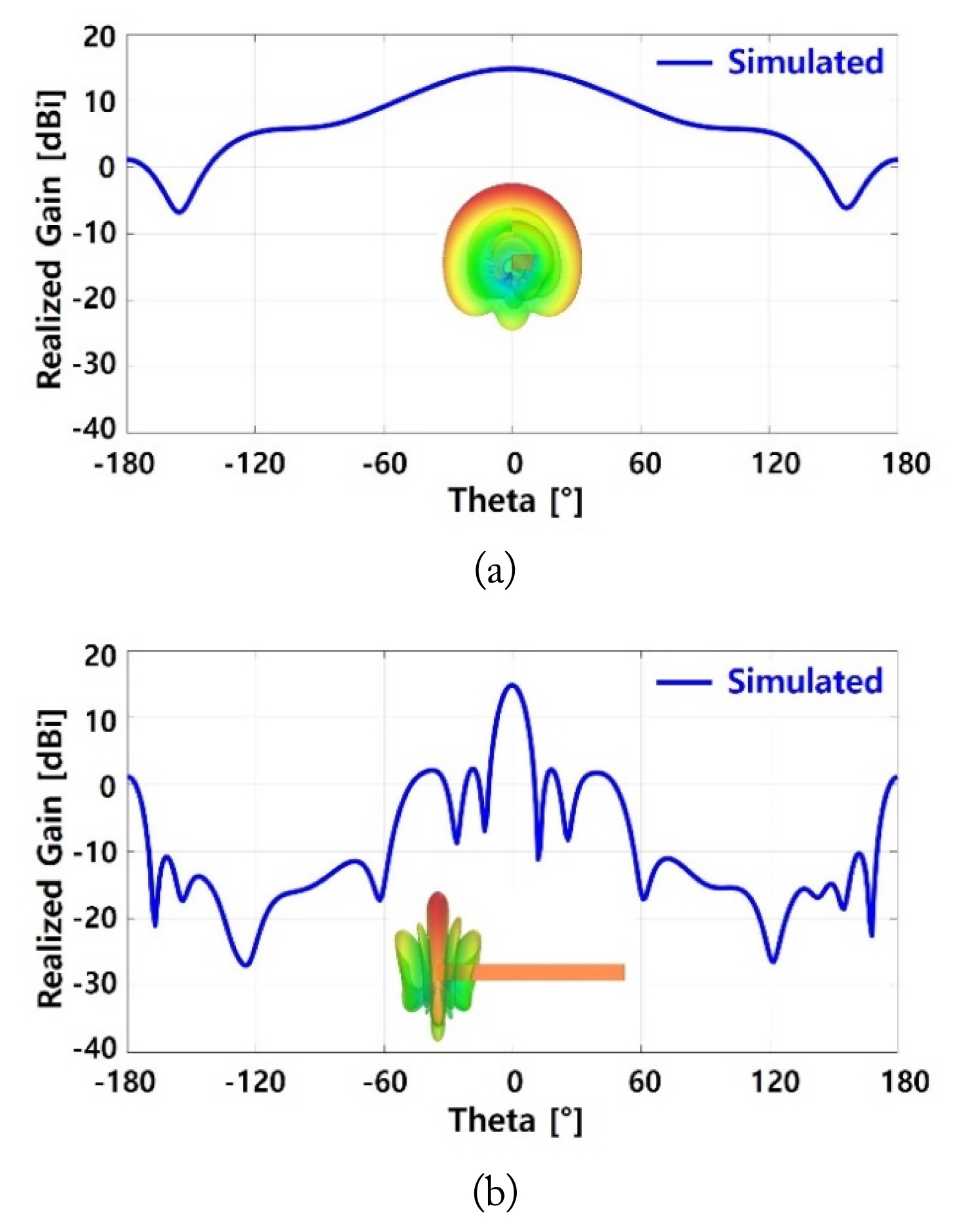
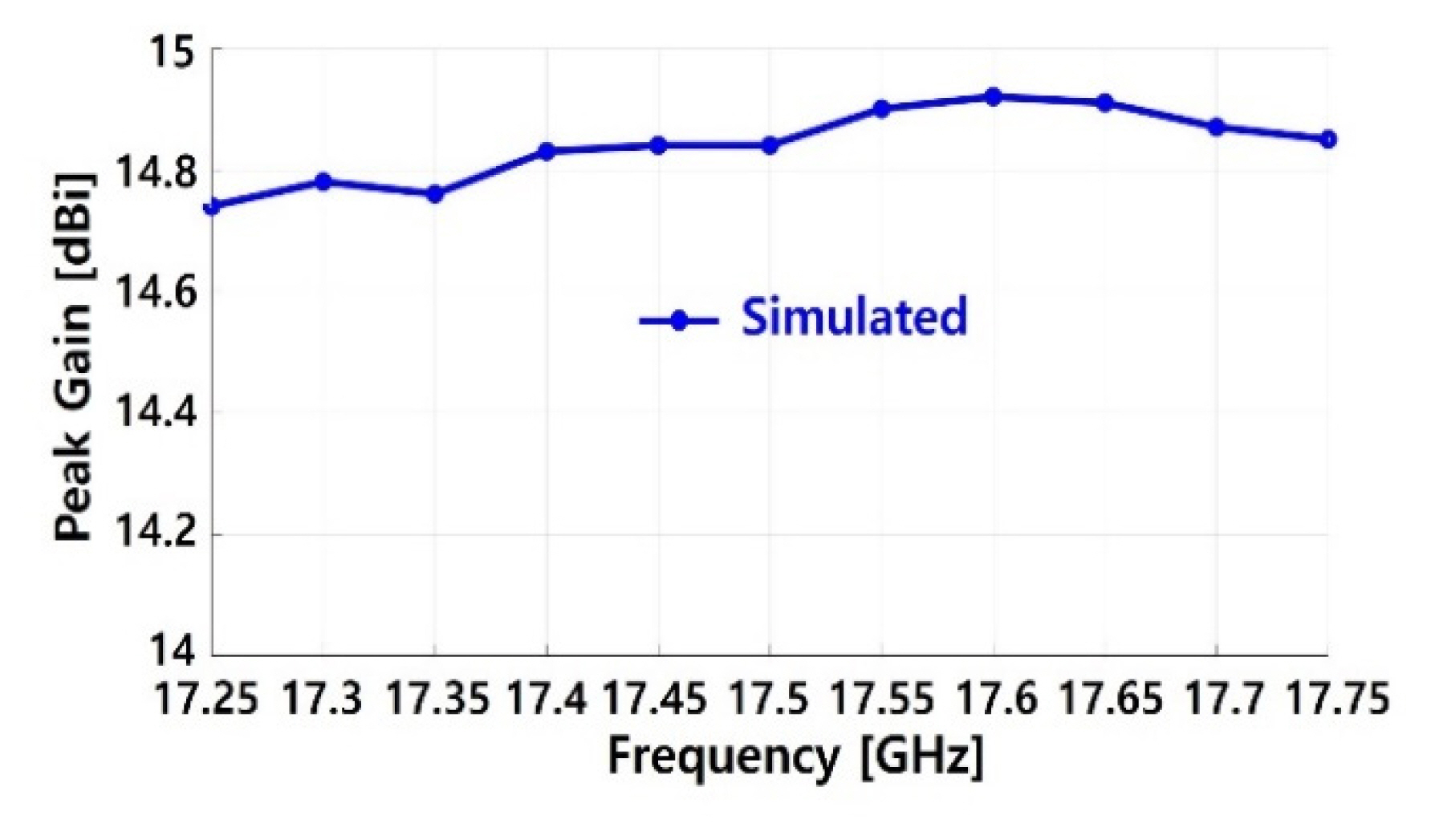
The proposed 6 × 26 array does not have a single-layer structure but rather a double-layer structure. For the proposed double-layer 6 × 26 slotted waveguide array antenna, the length of the broad and narrow walls of the waveguide are recalculated from 11.33 mm to 11.025 mm and from 5.67 mm to 6 mm, respectively, to control the beamwidth of the elevation and azimuth. Fig. 7 shows the structure and parameter information of the feeding slotted array antenna with a cavity structure. The design is optimized to minimize the coupling between the slots and to obtain an isotope by slanting the feeding slots. Phase control improves the frequency bandwidth and gain by minimizing the change in the imaginary part of the impedance. The structure in Fig. 7 allows the current to be evenly distributed from one slot placed at the front of the center to the 13 resonance slots placed symmetrically around it in the radiation field. Table 3 lists the slot parameters for the feeding slotted waveguide array antenna with a cavity structure. The sizes of all slots placed at the front of the station are the same in length (Sl) and width (Sw). The distance between the slots (Ss) is consistent, and the rotational angles of the six slots are denoted as #1, #2, #3, #4, #5, and #6. Fig. 8 illustrates the results of the voltage standing wave ratio (VSWR) simulated experiments for the feeding slotted waveguide array antenna with a cavity structure. The simulated VSWR obtains good properties of approximately 1.5 or less in the target frequency band. The VSWR results are good because they reduce the phase difference by minimizing the interconnection of the feeding slots. Fig. 9(a) shows the XZ-plane radiation pattern of the feeding slotted waveguide array antenna simulated at 17.5 GHz, with a peak gain of 14.84 dBi at 0° and a half-power beamwidth (HPBW) of 80.22°. Fig. 9(b) shows the YZ-plane radiation pattern of the feeding slotted waveguide array antenna simulated at 17.5 GHz, with a peak gain of 14.84 dBi at 0° and an HPBW of 11.12°. Fig. 10 illustrates the peak gain versus frequency of the feeding slotted waveguide array antenna, which exhibited high-gain characteristics of about 14.7 dBi or more in the target frequency band. This is a good VSWR characteristic in the target frequency band. Therefore, this structure shows a high-gain characteristic broadband, even when combined with a radiating antenna structure.
III. Fabrication and Measurement
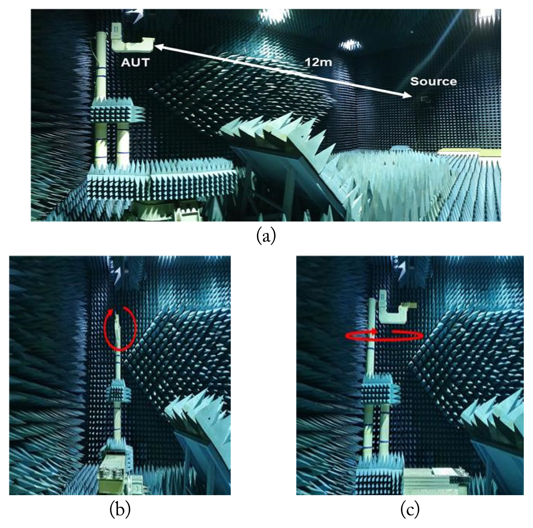
Based on the design results of the feeding slot array waveguide antenna and the radiating antenna structure, the 6 × 26 slotted waveguide array antenna was fabricated, as shown in Fig. 11. Fig. 12 shows photographs of the anechoic chamber and the measurement of the fabricated antenna.
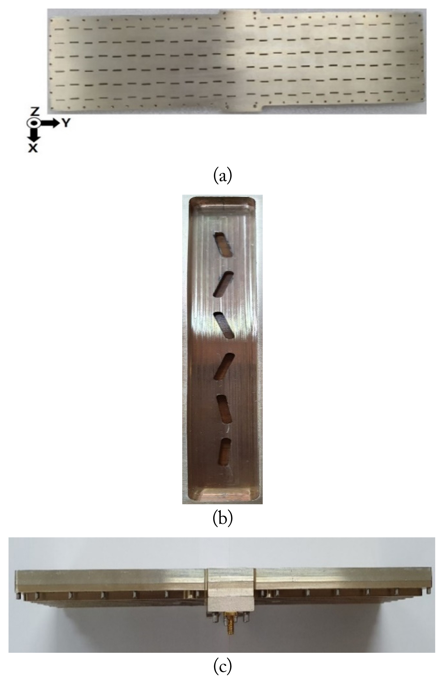
Fig. 11(a), 11(b), and 11(c) show the fabricated radiating antenna of the 6 × 26 slotted waveguide array antenna, the fabricated feeding antenna, and the side view of the 6 × 26 slotted waveguide array antenna having a total electrical length of 353.7 mm, respectively.
Fig. 12(a) shows the interior of the anechoic chamber (16 m × 11 m × 9.5 m) for the antenna measurement, particularly the source and the antenna under test (AUT) installed therein. This chamber has a measurable frequency bandwidth of 400 MHz–24.5 GHz. Fig. 12(b) and 12(c) show the setup for the measurement of the AUT. The red arrow indicates the positioner’s rotating direction for measuring the XZ-plane and the YZ-plane of the radiation pattern.
1. Measurement of the VSWR
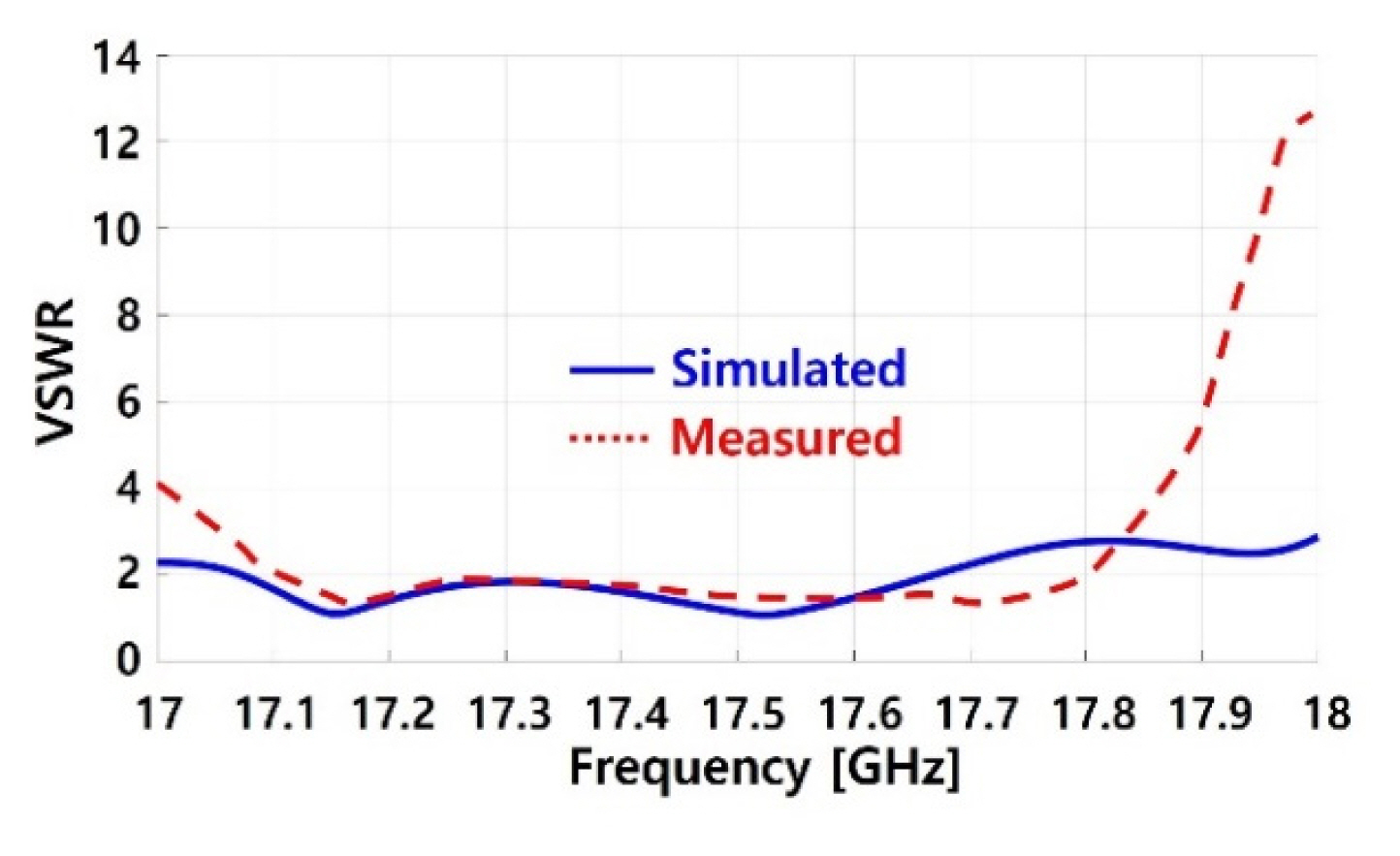
Fig. 13 compares the simulated and measured VSWRs of the fabricated 6 × 26 slotted waveguide array antennas built using vector network analyzers. The blue solid line and the red dotted line represent the simulation and measurement results, respectively, indicating a good match between the two. The VSWR is measured at less than 2 at the target frequency band of 17.25–17.75 GHz, showing excellent characteristics. This result indicates that the proposed structure can exhibit excellent properties even when combined with a radiating antenna because of the excellent VSWR characteristics of the feeding antenna designed by simulation, resulting in low feed loss.
2. Measurement of Radiation Patterns
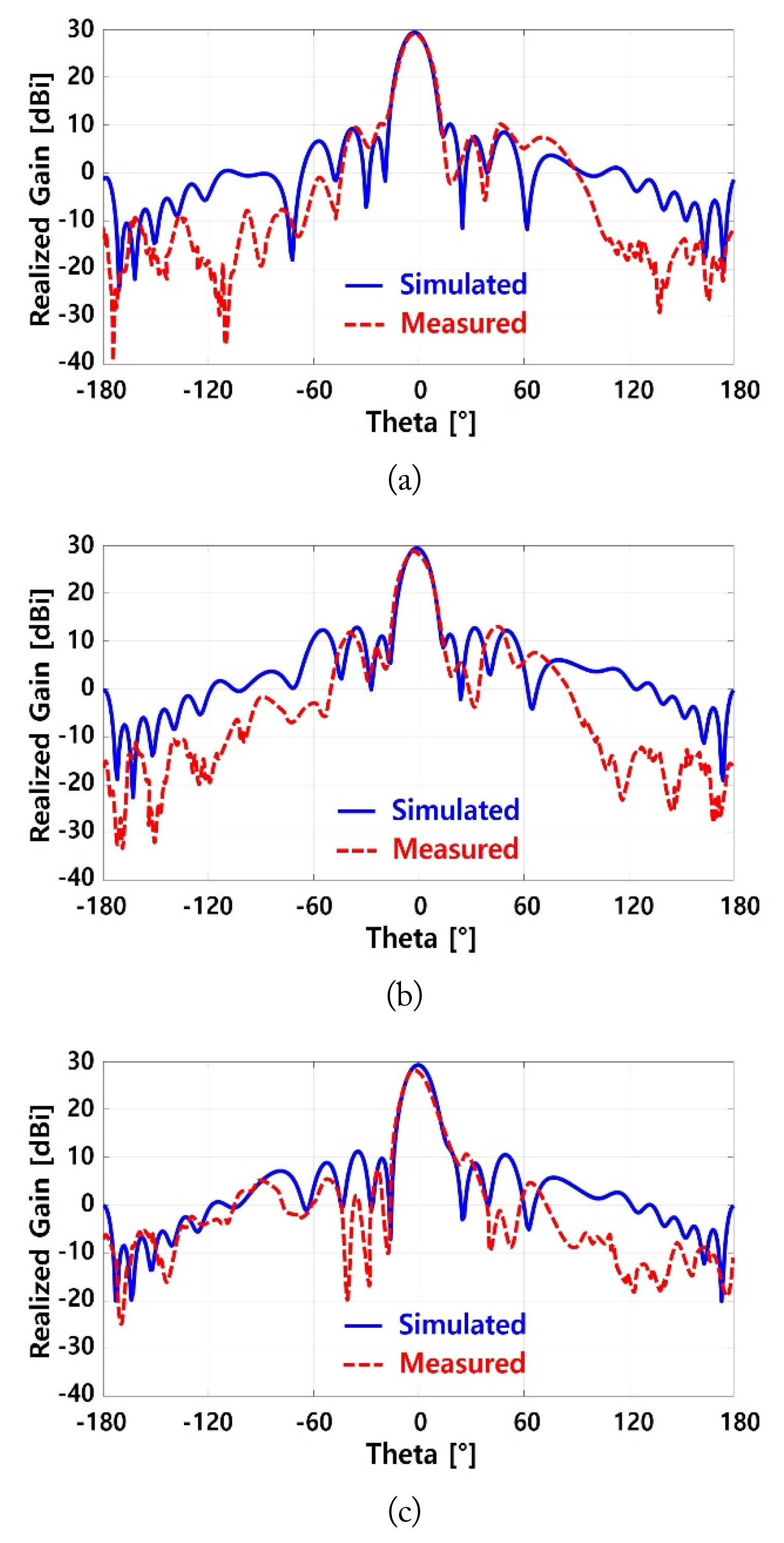
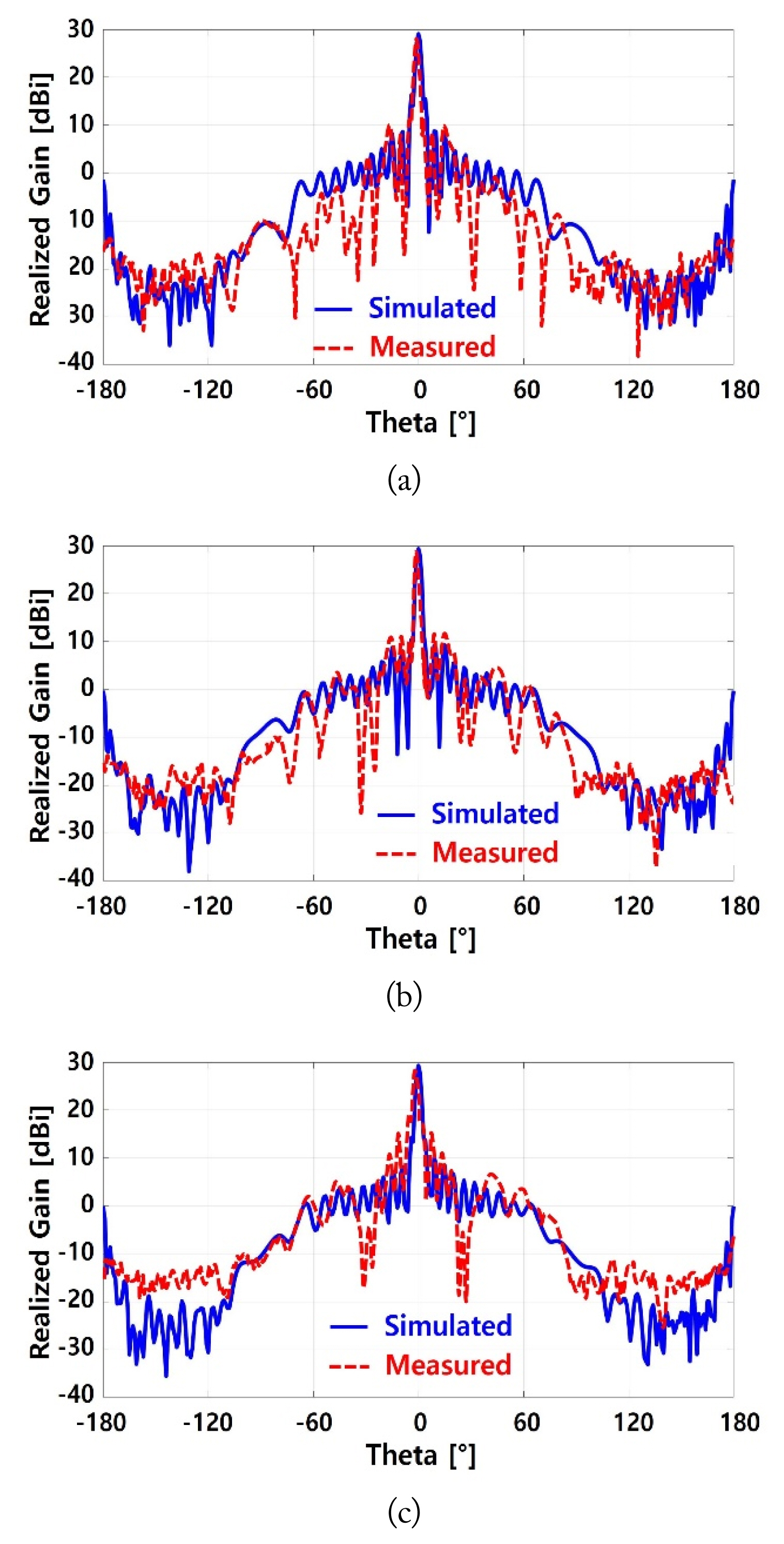
Figs. 14 and 15 compare the radiation patterns on the XZplane and the YZ-plane, respectively, of each frequency band of the 6 × 26 slotted waveguide array antenna measured by the anechoic chamber. The magnitude of the measured gain value is converted to that of the absolute gain value.
Fig. 14 shows the radiation patterns on the XZ-plane measured for each frequency. The elevation (XZ-plane) is wide because of the nature of the wave monitoring radar system, which detects the exact height of the waves moving up and down in real time. Fig. 14(a) shows the peak gain of the beam measured at 17.25 GHz, with a peak gain of 28.79 dBi at −1°. The HPBW is 13.86°, and the sidelobe level is 19.44 dB.
Fig. 14(b) shows the radiation patterns measured at 17.5 GHz, with a peak gain of 28.92 dBi at −1°. The HPBW is 13.75°, and the sidelobe level is 20.07 dB. Fig. 14(c) shows the radiation patterns measured at 17.75 GHz, with a peak gain of 28.14 dBi at −2°. The HPBW is 13.86°, and the sidelobe level is 21.23 dB.
Fig. 15 shows the radiation pattern with the azimuth direction on the YZ-plane. For the wave monitoring radar system, an antenna is designed to have a narrow azimuth relative to the elevation, as it rotates 360°. Fig. 15(a) shows the radiation patterns on the YZ-plane measured at 17.25 GHz, with a peak gain of 28.48 dBi at −1°. The HPBW is 2.42°, and the sidelobe level is 15.69 dB. Fig. 15(b) shows the radiation patterns measured at 17.5 GHz, with a peak gain of 28.67 dBi at −1°. The HPBW is 2.78°, and the sidelobe level is 17.46 dB. Fig. 15(c) shows the radiation patterns measured at 17.75 GHz, with a peak gain of 28.12 dBi at −1°. The HPBW is 2.41°, and the sidelobe level is 8.69 dB. Table 4 shows a comparison of the peak gain results between the measured and simulated radiation patterns. Figs. 14 and 15 show that the measured and simulated radiation patterns matched well at the location of the main beam.
3. Comparison of Peak Gain
Fig. 16 shows a comparison of the simulated and measured peak gains at the target frequency band of 17.25–17.75 GHz at a 50-MHz interval. The blue solid line and the red dotted line represent the simulated and measured peak gain values for the fabricated antenna. For the fabricated antenna, the measured gain is over 28 dBi, which is 1 dBi lower than that of the simulation result. This difference is due to the fine mechanical errors that occur in the length, width, offset, and spacing between the slots, resulting in differences between the overall theoretical and actual results. This results in a large difference of about 1 dBi in the high-frequency band. Nevertheless, the measured gain results are good, considering that they are maintained at a value higher than 28 dBi.
IV. Conclusion
In this paper, a 17-GHz band 6 × 26 slotted waveguide array antenna was designed. To obtain a broad frequency bandwidth and high-gain characteristics, the first step was to design a 1 × 26 slotted waveguide array antenna with a double-layer structure. Then, a 6 × 26 slotted waveguide array antenna with recalculated lengths of the broad and narrow walls of the waveguide for elevation and azimuth control was designed, fabricated, and analyzed. The fabricated antenna’s VSWR achieved excellent properties of approximately 2.0 or less, which is within the target bandwidth of 500 MHz, and the measured radiation patterns agreed well with the simulated patterns. Specifically, the HPBW values of the XZ-plane and the YZ-plane were 13.75° and 2.78°, respectively. The peak gain of the measured and simulated antennas showed similar characteristics. The measured gain remained higher than 28 dBi at a center frequency of 17.5 GHz. These results are expected to play a major role in the development of wave monitoring radar antennas and in the safe and economic operation of autonomous vessels in the future.