Design of a 0.5–18 GHz Wideband Switching Matrix Box for Electronic Support Measurement
Article information
Abstract
In this paper, we design and fabricate a broadband switching matrix box with low-noise figure, flat gain characteristics, and reliability by applying the chip-and-wire process using a bare-type MMIC device. To compensate for the mismatch among many components, the limiter, switch, amplifier, and power divider, which are suitable for sub-band frequency characteristics, are designed and applied to the matrix box. The matrix box has three submodules that are phase-matched for each frequency band and one built-in test (BIT) submodule to select the BIT path for calibration. Phase-matched RF semi-rigid cables of different lengths are used to connect to the external interface of the matrix box. The main RF line is a dielectric substrate, RT/Duroid 5880, with a relative dielectric constant of 2.2 and a dielectric thickness of 0.127 mm. The BIT path is a dielectric substrate, ceramic alumina (AI2O3), which has a relative dielectric constant of 9.8 and a dielectric thickness of 0.254 mm. In the wideband switching matrix box, the gain is from −1.71 dB to −2.69 dB at LB (input frequency, 0.5−2 GHz), with a flatness of 1.0 dB. The gain is from +14.8 dB to +12.4 dB at MB (input frequency, 1−6 GHz), with a flatness of 2.4 dB. The gain is from +12.6 dB to +9.4 dB at HB (input frequency, 6−18 GHz), with a flatness of 3.2 dB. The measured values of the noise figure are 2.69 dB at low band, 4.4 dB at medium band, and 5.95 dB at high band with a maximum value. The measured value of phase matching at high band is 7° with a maximum value.
I. Introduction
Electronic warfare is largely classified into three categories: electronic support, electronic attack, and electronic protection. The electronic support field of electronic warfare is a function that identifies the electromagnetic energy emitted by the enemy, such as search, tapping, and direction detection. To detect the fine signal of the target, all frequencies should be received and analyzed as much as possible. In other words, it is necessary to search for and analyze all the frequencies used in the satellite frequency and the group from the mobile communication frequency that is used commercially. In the future, electronic support equipment will be developed into various platforms, such as portable and remote control. This is expected to change such characteristics as frequency use, digital modulation, and data coding. Therefore, techniques such as miniaturization, weight reduction, and broadband search processing are required [1].
Electronic support (ES) equipment for electronic intelligence requires receivers with a multi-octave bandwidth, and the receivers required for most electronic warfare system (EW systems) have very strict performance requirements.
In addition, each component is connected using a microstrip line or a short RF cable for fabrication and testing. Additional tuning is also required to reduce mutual mismatching [2–4]. As previously discussed, the broadband switching matrix module connected to the rear end of the antenna in the electronic support equipment system is a key element determining the overall system performance.
In this paper, we designed and implemented a sub-unit module in which the frequency of 0.5–18 GHz is divided into three bands of LB (low band, 0.5–2 GHz), MB (medium band, 1–6 GHz), and HB (high band, 6–18 GHz). The design approach and contents proposed in this paper are as follows.
First, the switching matrix module for receiving multiple antenna signals individually consists of four channels in each band. Each channel is designed to have three input ports and one output port; therefore, each channel needs 12 antenna connections.
Second, to improve the overall noise figure characteristics through a low-noise amplifier (LNA) for MB and HB except LB, we used a bare-type switch and low-loss PCB to minimize loss to the LNA front end.
Third, a broadband distributor (1:4) was designed to select the first switch to check whether each channel is operating normally. In this case, the distributor is located at the center of the module so that the built-in test (BIT) signal can be supplied to the same position in each channel. To secure high reliability in a high-frequency band, alumina material was used having a high permittivity (ɛr = 9.8).
The direction of arrival is determined using a point in which a received signal has a phase difference according to a distance from a reference antenna. In this case, self-phase matching in a plurality of channels existing in a receiver should be performed [5]. The requirements of the electronic warfare system and the specifications proposed in the paper are shown in Table 1.
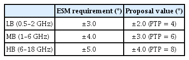
Comparison table between the ESM system and the proposed system
II. Wideband Switching Matrix Structure
Fig. 1 shows the configuration of a broadband switching matrix box required for ES systems, including switches, limiters, and LNAs. As shown in the diagram, it is designed to collect radio waves from low band to high band, and it is possible to correct the RF line and the box part (BIT PATH) to separately secure the built-in test equipment port [6].

Block diagram of the switching matrix box.
The product to be studied is a broadband switching matrix box, which is designed and implemented by dividing the frequency of 0.5–18 GHz into three submodules (LB, MB, and HB). Each submodule is connected to the back of an antenna. Each port is defined as follows:
All J ports are connected to the antenna.
All P ports are connected to a filter bank except for P13 and J4.
The ports of P13 and J4 are for receiving signals from an external synthesizer.
Each submodule operates according to an external control command. For example, when a command to select an antenna path is received, all bands move equally.
It is necessary to amplify and select a path, and the phase-matching characteristic should be excellent for each path. Each submodule has four RF channels, and each channel has three RF input ports and one BIT port.
The reason for separating the submodules (LB, MB, and HB) in the box is that the antennas connected in the system units are divided into sub-bands rather than into designing and manufacturing broadband (0.5–18 GHz). In addition, phase matching is required for each channel until the analog-to-digital converter is taken by the corresponding path in addition to the front-end (FE) module in the ES system. Fig. 2 shows the phase-matching calculation between the FE module for the four paths on the system side and each corresponding path (matrix box) on the downstream side, including the RF cable required for connection. What is important here is that even if the system phase matching can be adjusted to 4° or less, the phase matching of the antenna path itself must also be matched within 5° (matrix box; a 20° difference is not acceptable).
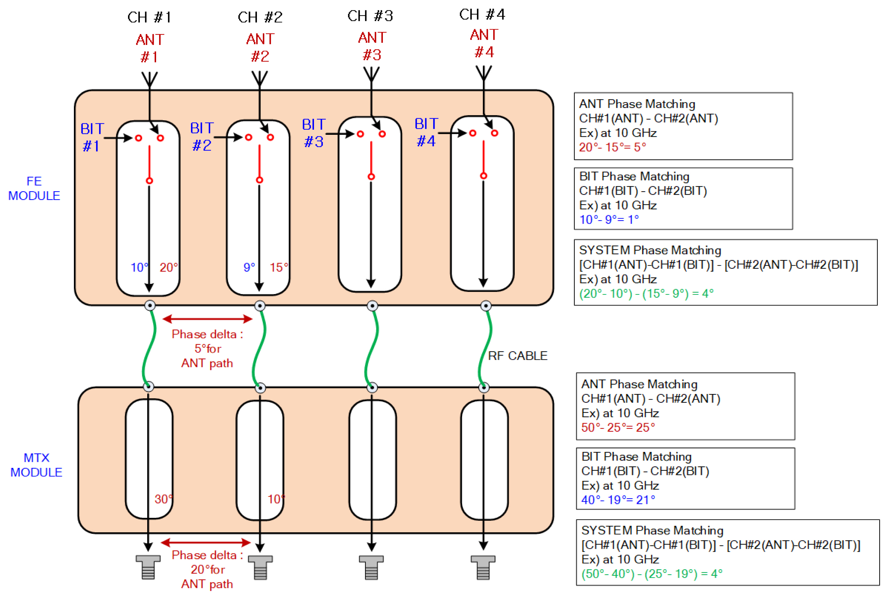
Block diagram for the phase-matching calibration from the FE module to the MTX (matrix) module.
III. Design and Simulation
1. Feed-thru Design for the H Structure
In the module form of an H structure (upper layer is RF line; lower layer is power supply circuit), a glass bead (signal connector) is used to prevent loss and impedance mismatch in the upper layer (RF path). The signal should be supplied vertically [7]. Fig. 3 shows the design of the feed-through in the vertical structure for the simulation. As a result of the simulation in Fig. 4, the insertion loss is 0.13 dB at 18 GHz, and the return loss is 23.9 dB or less.
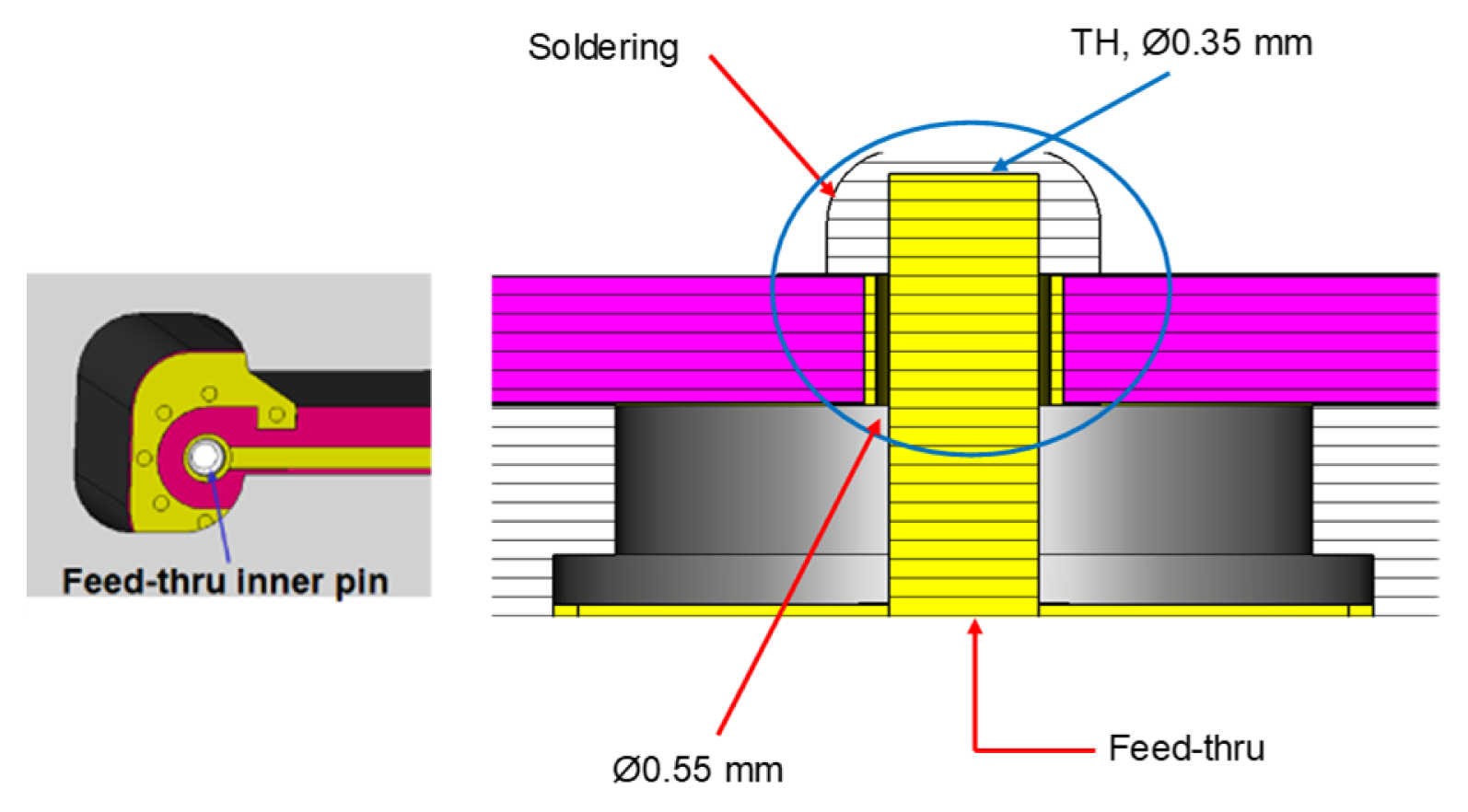
Side image of the vertical structure using feed-through.
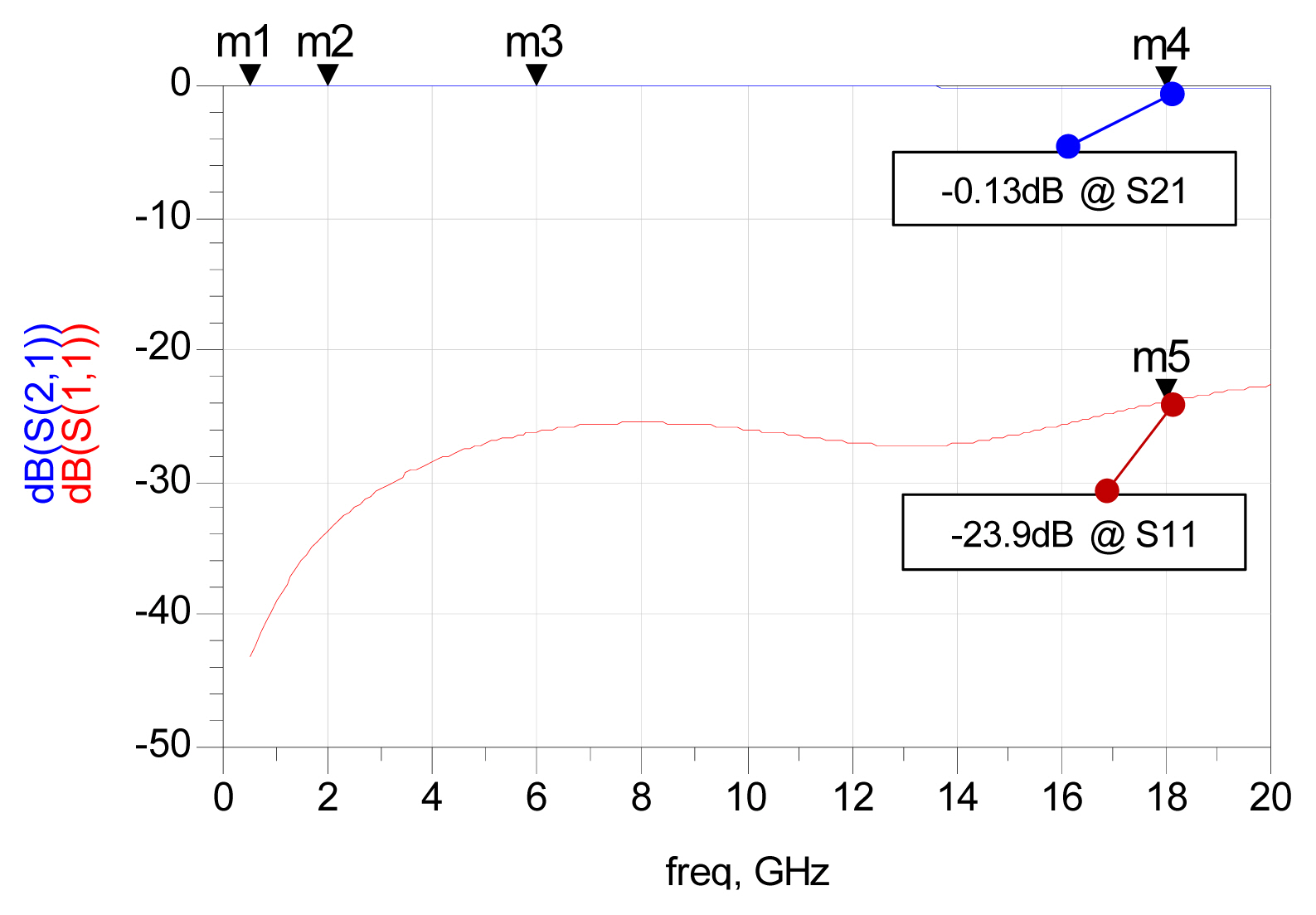
Simulation results in the vertical structure using feed-thru.
2. Limiter Design for the MB (1–6 GHz) Frequency
Among the RF signals received from the antenna, a limiter is designed and applied to the MB (1–6 GHz) submodule to protect the LNA part located at the beginning of the module when a high signal is applied. The limiter circuit, including the inductor and the PIN diode, uses the inductor to remove the minute current while operating the PIN diode when the PIN diode (MG20T47) receives high power. Figs. 5 and 6 show the simulation circuit, including the PCB artwork and a graph of the leakage power, according to the input power of the limiter circuit. The input power increases linearly up to the input of +10 dBm, and the output power is suppressed little by little from the input power. When the input power is +30 dBm, the output leakage amount is about +16.6 dBm. The results show that the internal LNA components can be protected even if unwanted external signals are introduced up to +30 dBm.
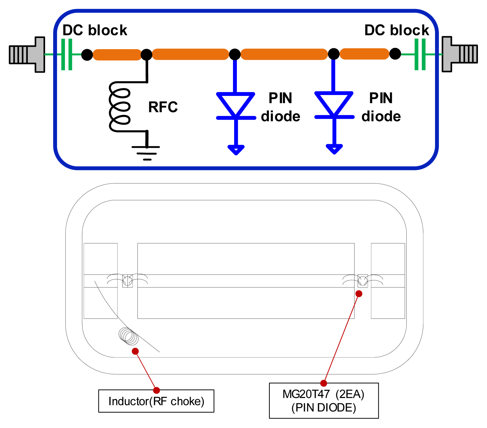
Simulation circuit (top) and PCB artwork (bottom) including the inductor and the PIN diode.

Simulation result for the limiter circuit.
3. Wideband Power Combiner Design
A broadband two-way power combiner is needed to branch the BIT signal from the box to multiple channels. This is necessary to obtain normal RF presence and calibration. In addition to using a typical 3-dB Wilkinson power divider, a multistage circuit is used to operate the wideband frequency [8].
In the MB (1–6 GHz) frequency, the quarter wavelength is difficult to apply to a submodule with a limited size.
Therefore, a thin film resistor is designed as an R divider with 18 Ω, which can be applied to an alumina PCB. Fig. 7 shows the artwork designed with an alumina PCB—based on a ceramic alumina (AI2O3) of 0.508 mm with a specific inductive capacity of 9.8—to distribute one input to four using the three-stage power combiners. As shown in the simulation result of the power combiner structure in Fig. 8, the insertion loss is about 11.8 dB, and the return loss is less than 22.7 dB at the maximum frequency of 6 GHz for MB.

PCB artwork for the three-stage power combiner.
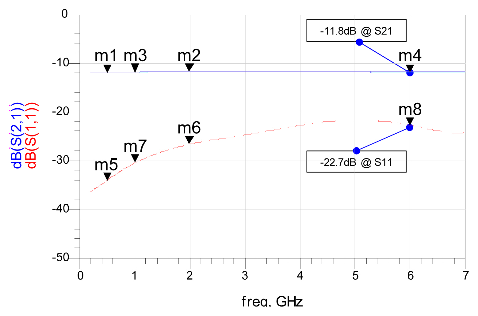
Simulation results for the three-stage power combiner.
4. Wire Bonding Analysis
To make mutual connections among numerous transmission lines and parts in the very wide ultra-high-frequency range up to 18 GHz without any loss or impedance mismatching, the design should meet the requirements for PCB spacing and the number and angles of wire bonding. As the PCB types required for wideband receiver modules are the RT/Duroid 5880 (Rogers Corp., Chandler, AZ, USA) 0.127 mm (specific inductive capacity = 2.2) and alumina-based ceramic alumina (AI2O3) 0.508 mm (specific inductive capacity = 9.8), the insertion loss and standing wave ratio characteristics vary within the operating frequency (0.5–18 GHz) band according to the spaces between the PCBs.
Fig. 9(a) shows a 3D structure modeling according to different PCB spacings (left side, 150 μm; right side, 380 μm) between the alumina and the Duroid PCB. Bonding is commonly applied to two places. Fig. 9(b) shows the results of a simulation conducted when the PCB spacing is 380 μm on the right side. A maximum insertion loss of −0.41 dB is shown at 18 GHz and a maximum return loss of −10 dB at 15.7 GHz.

(a) Different PCB spacing structures (380 μm on the right side). (b) Simulation results when the PCB spacing is 380 μm on the right side.
Fig. 10(a) and (b) illustrate the 3D structure and simulation that narrows the interval on the right side, with a low insertion loss (−0.34 dB at 18 GHz) and a good return loss (−15 dB at 15.7 GHz). Therefore, the signals can be transmitted within the band without a large signal loss. This result shows the minimum gap to secure the performance up to 18 GHz operated by checking the characteristic difference according to the PCB spacing when connecting PCBs of different materials using wire bonding.

(a) Different PCB spacing structures (150 μm on the right side). (b) Simulation results when the PCB spacing is 150 μm on the right side.
IV. Fabrication and Measurement
A GaAs MMIC chip was mounted on a gold-plated substrate to provide good grounding. A high-frequency Duroid PCB was placed around the chip to connect the DC bias, and input and output lines were wire-bonded using the chip-and-wire process [9].
A broadband switching matrix box was made with 36 RF input ports (0.5–18 GHz), 12 output ports (0.5–18 GHz), and 1 external BIT input port. We also designed and manufactured an RF cable (semi-rigid type) to transmit the submodules inside. Each submodule was assembled by submodule units. Each submodule used a bare-type MMIC and RT/Duroid 5880 (thickness, 0.127 mm) PCB to achieve miniaturization and weight reduction [8]. The frequency of the −18 GHz band was transferred through the transmission line so that the signal was transmitted without loss or distortion. To overcome the low frequency and narrow bandwidth limitations of existing products, instead of fabrication using general package components, bare-type MMIC devices with high operating frequency and wide bandwidth were used to directly mount the components to the housing. The chip-and-wire process was applied to minimize mismatch.
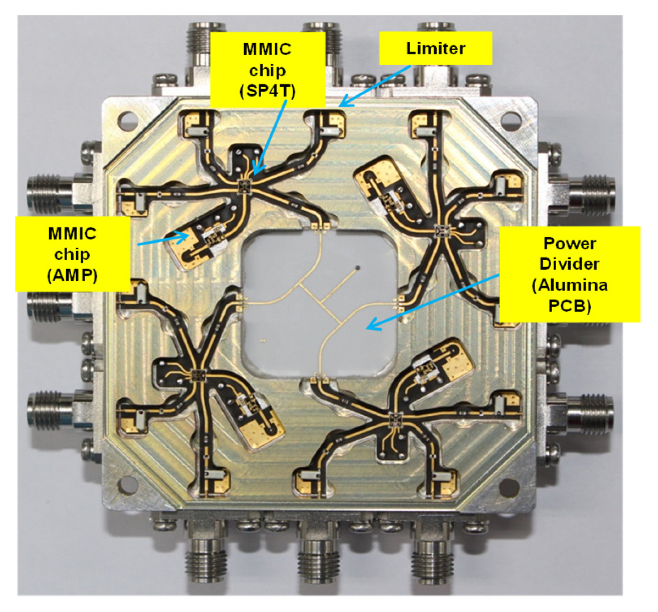
Fig. 11 shows the assembled inner figure of the whole box with four submodules (LB, MB, HB, and BIT), the control board, and the RF semi-rigid cable. Many cables are needed to connect the ports of the inner submodule to the interface of the outer box. Figs. 12–14 show the inner shape of each submodule.
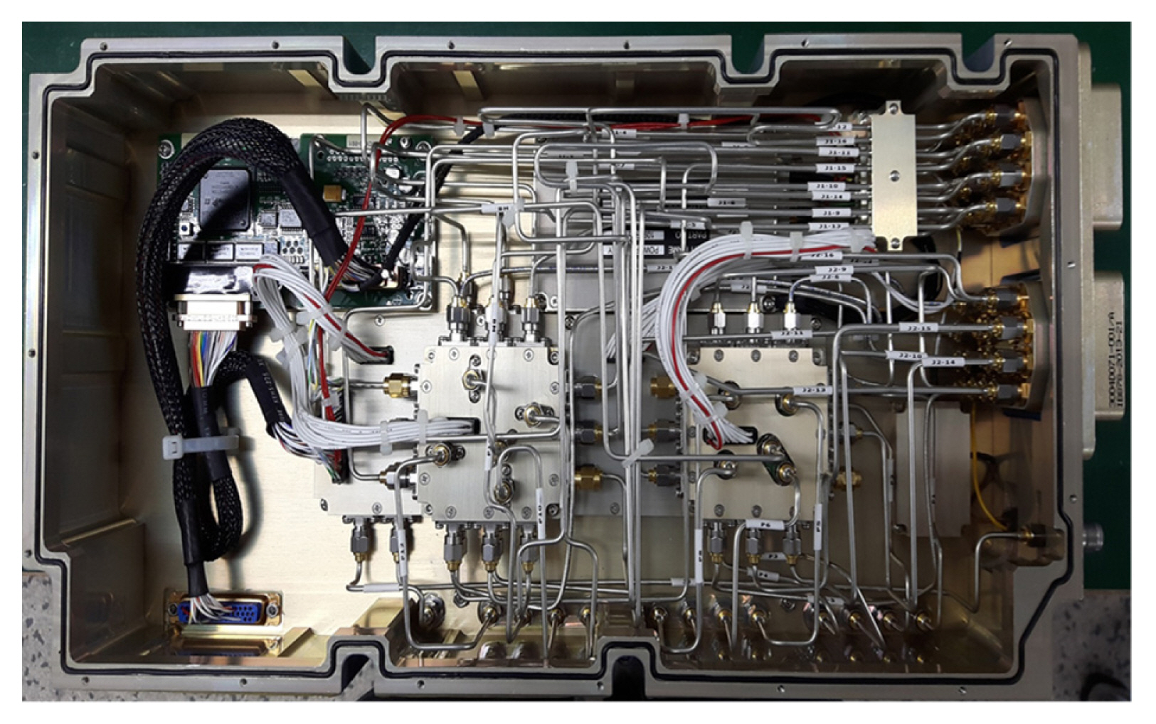
Photograph of the broadband switching matrix box (0.5–18 GHz).
Photograph of the LB submodule (0.5–2 GHz).
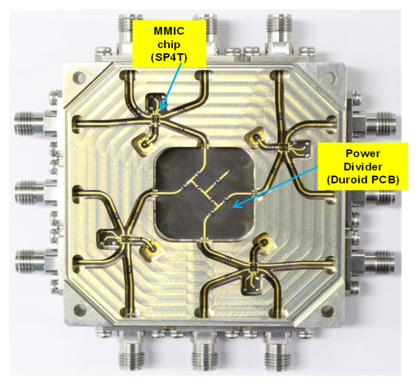
Photograph of the MB submodule (1–6 GHz).

Photograph of the HB submodule (6–18 GHz).
To perform phase matching between the submodules, the corresponding paths were tuned individually using the tuning pad, the reference channel was normalized, and the phase difference of the other channels was determined. Fig. 15 shows a photograph of the tuned form.
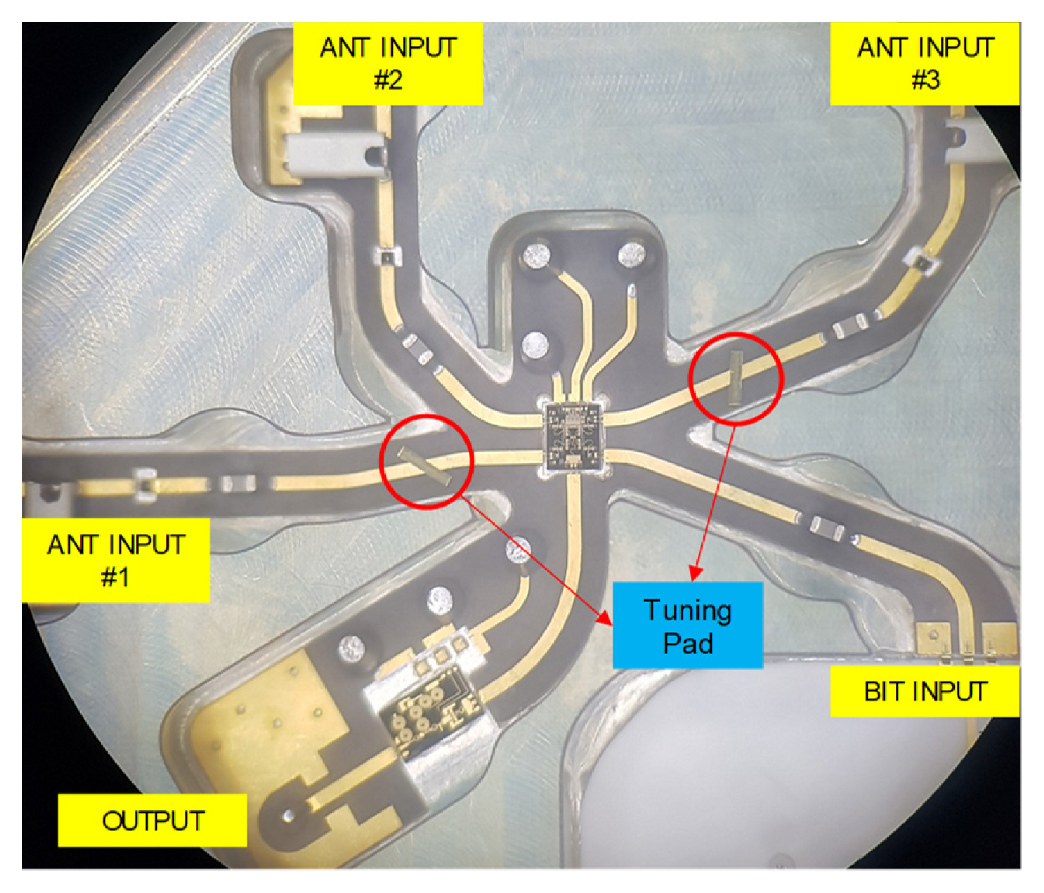
Photograph of the tuned photos for the MB submodule (1–6 GHz).
1. GAIN and Return Loss Measurement Results
Fig. 16 shows the gain and reflection coefficient graphs for the LB path (frequency, 0.5–2 GHz), with a gain of at least −2.69 dB in the band, a gain flatness of 1.0 dB at maximum, and an input reflection coefficient of −15.8 dB.
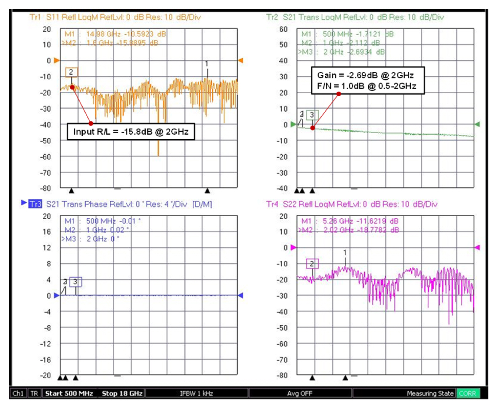
Results of the measurement of gain and return loss (LB).
Fig. 17 illustrates the gain and reflection coefficient graphs for the MB path (frequency, 1–6 GHz), with a gain of at least +12.4 dB in the band, a gain flatness of 2.4 dB at maximum, and an input reflection coefficient of −12.0 dB.
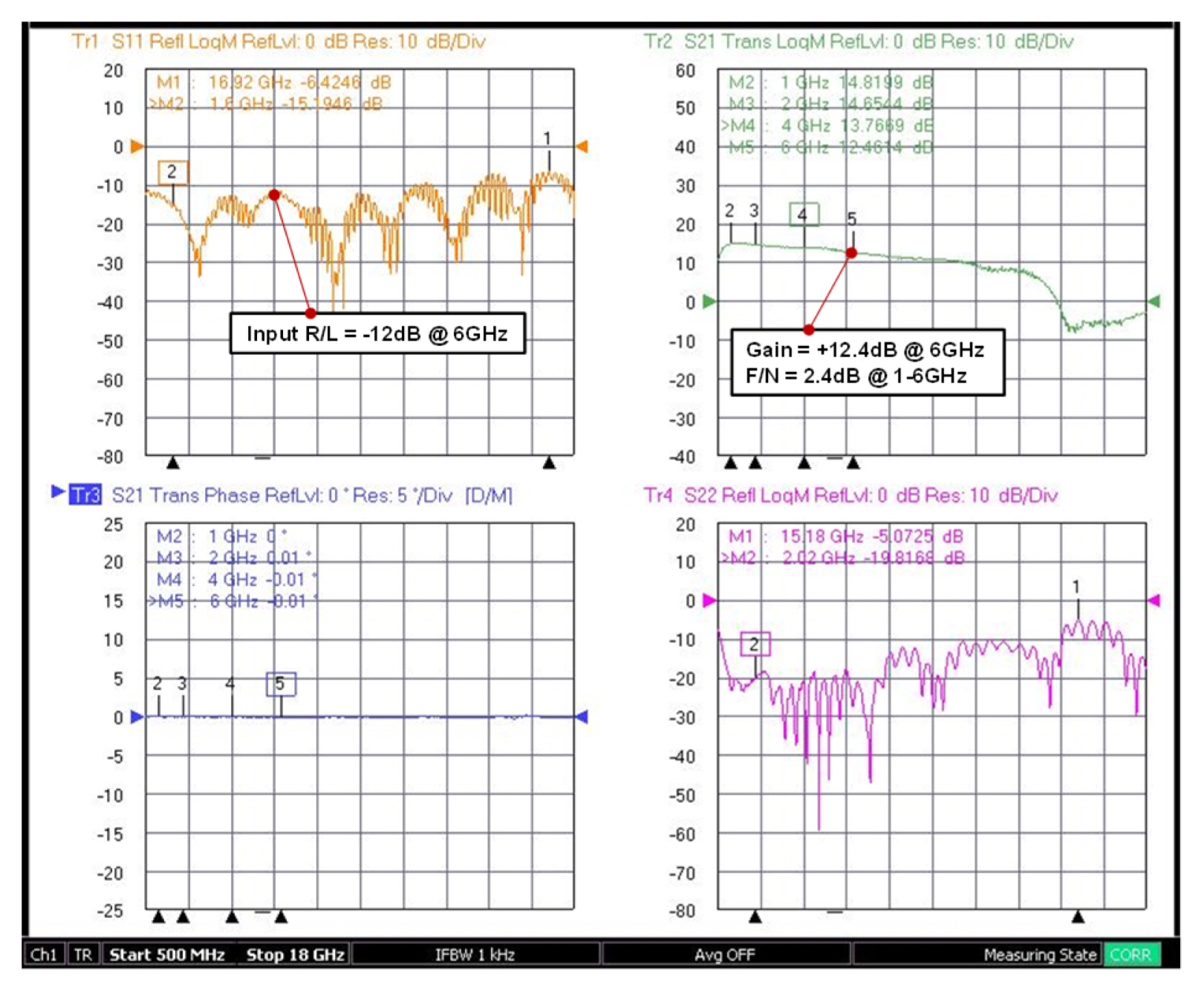
Results of the measurement of gain and return loss (MB).
Fig. 18 shows the gain and reflection coefficient graphs for the HB path (frequency, 6–18 GHz), with a gain of at least +9.4 dB in the band, a gain flatness of 3.2 dB at maximum, and an input reflection coefficient of −13.8 dB.
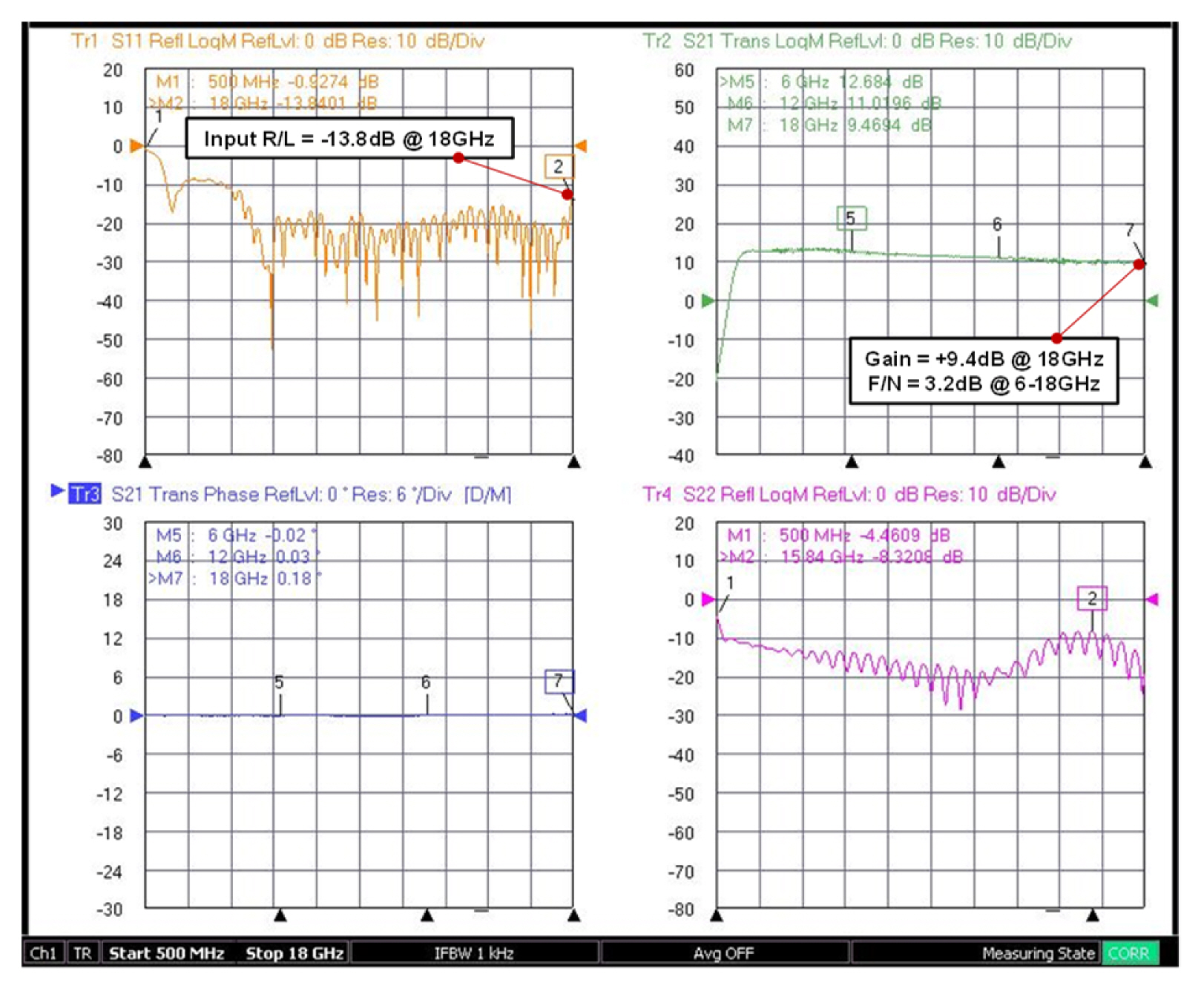
Results of the measurement of gain and return loss (HB).
Figs. 16–18 show the input R/L, gain and gain flatness, and output R/L characteristics in each band as a whole test result after mounting the submodules in the matrix box.
The measured results of each path are shown in Table 2.
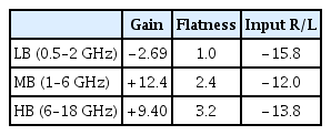
Summarized values of the main items for each frequency band (unit: dB)
2. NF Measurement Results
The noise figure of the receiver, which is the most important index, was measured as a pure insertion loss of 2.69 dB because there was no LNA in the RF line in the 0.5–2 GHz (LB) band. Figs. 19 and 20 show the noise figures of MB and HB at 4.4 dB in the 1–6 GHz band and 5.95 dB in the 6–18 GHz band.
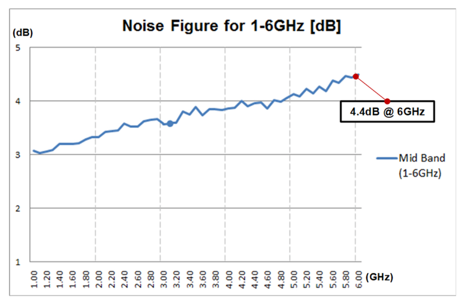
Results of the measurement of noise figure (MB).

Results of the measurement of noise figure (HB).
3. Phase Matching Measurement Results
Figs. 21–23 show the phase-matched measurements for each path for each sub-band. After normalizing antenna #1 to the reference path, the phase difference from the other paths (#2, #3, and #4) was measured. LB (0.5–2 GHz) was −2.3°, and MB (1–6 GHz) was from −2.2° to 5.0°. HB (6–18 GHz) showed the measurement results within 7°. This was the measurement result in the box unit, including the RF cable, which proved to be excellent in the broadband frequency.

Results of the measurement of phase matching (LB).
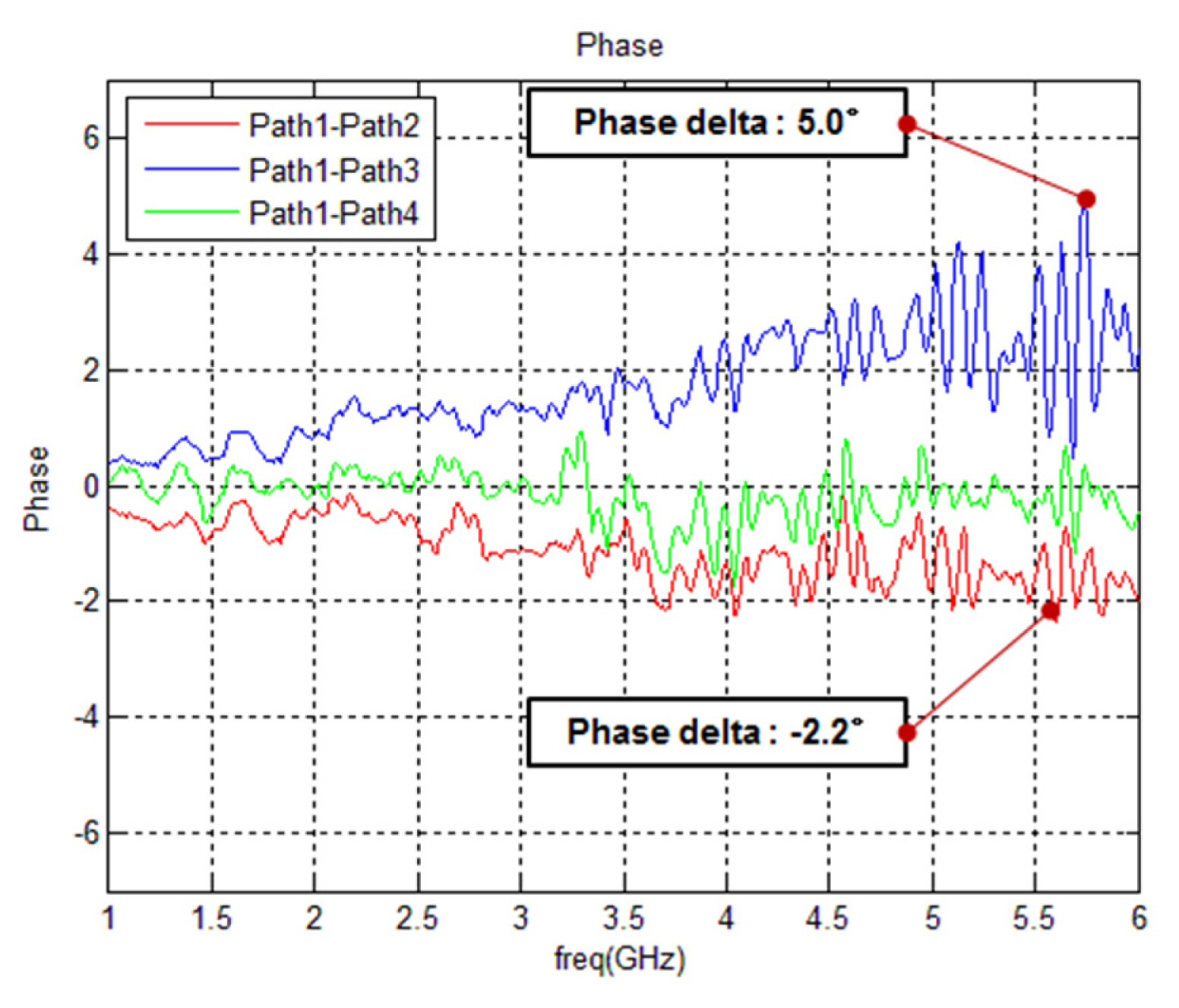
Results of the measurement of phase matching (MB).

Results of the measurement of phase matching (HB).
V. Conclusion
In this paper, we designed and fabricated a broadband switching matrix box with low-noise figure, flat gain characteristics, and reliability by applying the chip-and-wire process using a bare-type MMIC device. To compensate for the mismatch among many components, the limiter, switch, amplifier, and power divider suitable for sub-band frequency characteristics were designed and applied to the matrix box. The matrix box had three submodules that were phase-matched for each frequency band and one BIT submodule to select the BIT path for calibration. Phase-matched RF semi-rigid cables of different lengths were used to connect to the external interface of the matrix box.
The main RF line was a dielectric substrate (RT/Duroid 5880) with a relative dielectric constant of 2.2 and a dielectric thickness of 0.127 mm. The BIT path was a dielectric substrate, ceramic alumina (AI2O3) from ATC Co. (USA), and it had a relative dielectric constant of 9.8 and a dielectric thickness of 0.254 mm.
In the switching matrix box, the gain was from −1.71 dB to −2.69 dB at LB (input frequency, 0.5–2 GHz), with flatness about 1.0 dB. The gain was from +14.8 dB to +12.4 dB at MB (input frequency, 1–6 GHz), with flatness of 2.4 dB. The gain was from +12.6 dB to +9.4 dB at HB (input frequency, 6–18 GHz), with flatness of 3.2 dB.
The measured noise figure value was 2.69 dB with a maximum value at LB, 4.4 dB with a maximum value at MB, and 5.95 dB with a maximum value at HB.
The measured phase-matching value was −2.3° within the bandwidth at LB, from −2.2° to 5.0° within the bandwidth at MB, and 7° within the bandwidth at HB.
The proposed 0.5–18 GHz broadband switching matrix box can be applied to the switching matrix, which requires path selection at the back of the antenna of the ESM system.
References
Biography

Yuseok Jeon obtained his B.S. degree in electronic communication engineering from Chungju University, Chungju, Korea, in 2000, his M.S. degree in electronic engineering from Chungbuk National University, Cheongju, Korea, in 2004, and his Ph.D. in electronic and electric engineering at Dankook University, Yongin, Korea, in 2018. He worked as a director in the R&D division of Broadern Inc., Hwaseong, Korea, from 1999 to 2020. His research interests include the development of transceivers, receivers, and synthesizers using chip-and-wire processes for EW and radar system applications. He received the Korean Engineer Award in 2018 and the presidential citation for Science Day Government Rewards Science and Technology Promotion Section in 2020.

Jaejin Koo obtained his B.S. degree in electronic engineering from Soonchunhyang University, Asan, Korea, in 2006 and his M.S. degree from the Department of Electrical and Communication Engineering, Soonchunhyang University, Asan, Korea, in 2008. He worked as a general manager in the R&D division of Broadern Inc., Hwaseong, Korea, from 2008 to 2020. His research interests include the development of transceivers and receivers using chip-and-wire processes for EW and radar system applications.