


I. Introduction
Several nondestructive testing (NDT) techniques can be used to detect surface cracks in metal materials. These techniques include eddy current testing, AC (alternating current) field measurement, acoustic emission testing, and ultrasonic testing [1ŌĆō3]. Cracks in metal that are concealed by paint, composite laminates, corrosion protection substances, and rust can be detected easily using microwave techniques compared with other techniques. Studies have shown that nondestructive surface crack detection at the microwave and mm-wave frequencies is capable of detecting and sizing surface cracks in metals [4ŌĆō9]. In [4], an open-ended waveguide operating at 20 GHz was utilized as a sensor to detect smaller surface cracks, such as fatigue cracks from changes in the reflection coefficient. However, it can easily be affected by noise, air gap, and other factors [5]. To resolve this problem, several critical parameters of the open-ended waveguide technique have been investigated [6, 7]. To obtain a higher spatial resolution, the open-ended waveguide technique needs to be used at higher frequencies [8]. Alternatively, open-ended coaxial probes have also been examined [9]. Recently, resonant probes have been reported to design near-field sensors for crack detection in metallic materials [10]. Resonant probes provide many advantages compared with other probes based on measureing changes in the reflection coefficient. Several technologies with resonant probes for crack detection have been reported, including a microstrip linear resonator, a quarter-wavelength microstrip line, a dual-behavior resonator filter, and a complementary split-ring resonator [11ŌĆō14]. A more general review of state-of-the-art NDT techniques using microwave technologies is described in [15]. These techniques require a vector network analyzer (VNA), which makes the application of these types of probes difficult from a practical standpoint.
Conversely, cutoff cavity probes using forced resonance have been utilized for crack detection in metallic materials [16]. This method is called the forced resonance microwave method (FRMM). The advantage of this method is that VNA is not required, and thus the crack detection system can be established at low cost. FRMM consists of two stages: preparation and detection. It uses the current deviation from the resonance state for the cutoff cavity probe without a crack (corresponding to the preparation stage) and with a crack (corresponding to the detection stage). Therefore, knowledge of the current characteristics and the forced resonance modes of the cutoff-cavity probe in the preparation stage is needed as a reference to obtain the crack signals.
This paper presents the current states of the forced resonance of the cutoff cavity applied to crack detection using FRMM. The cutoff-cavity probe produces forced resonance by adjusting a control element. There are two kinds of forced resonance: series resonance (SR) and parallel resonance (PR). The SR causes a maximum current, and the PR and the region surrounding it produce sluggishly gradient currents. The steepest gradient currents occur around the SR. The minimum current occurs at non-resonance (NR) using the control element. Therefore, there are four types of current states in FRMM: maximum current (at the SR), minimum current (at the NR), rapidly changing current (around the SR), and slowly changing current (at the PR and around it). These current characteristics have been classified. The FRMM mainly uses SR, but PR and NR can also be used for crack detection. However, PR and NR are not as advantageous as SR. To verify the current state inside the cutoff cavity, the experimental results are compared with the theoretical results.
II. System Description
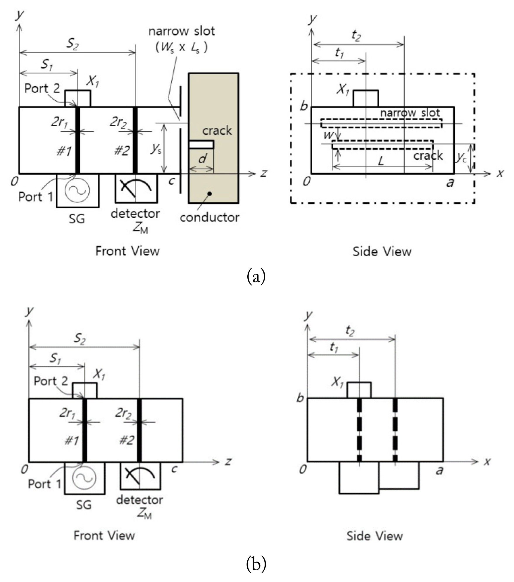
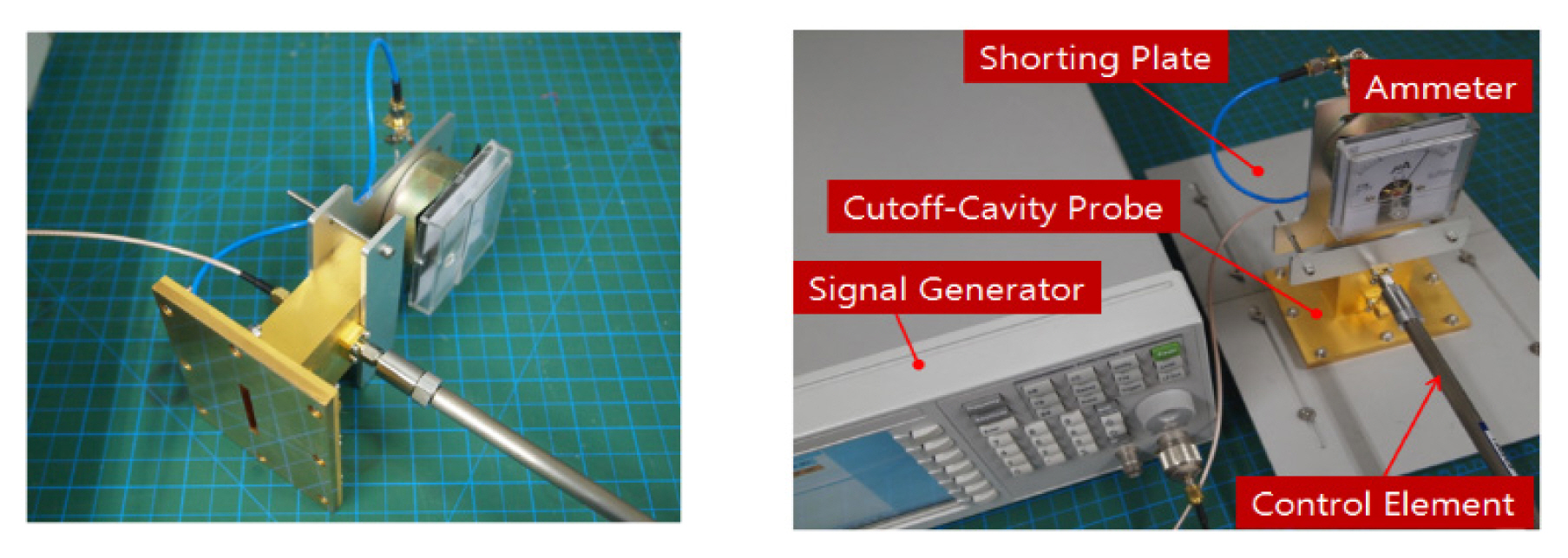
The geometry of the surface crack detection system is shown in Fig. 1. The detection system consists of four parts: (1) the cutoff cavity-backed narrow slot probe with internal posts #1 and #2, (2) the external control element jX1 for cavity resonance control, (3) the signal generator, and (4) the detector for reading the current states on post #2 and the crack signals. A voltmeter or an ammeter can be used as a detector. In Fig. 1(a), the probe and metal are presented separately, but in actual detection, they are in perfect contact. In the preparation stage, the slot is short, and the probe becomes a perfect cavity, as shown in Fig. 1(b).
The probe dimensions are chosen such that the cross-section a ├Ś b of the cavity corresponds to the cutoff condition for the waveguide of the same cross-section when the cavity is empty. For this reason, it is called a cutoff cavity. In the probe, a feed post (#1) of radius r1 is located at x = t1 and z = s1. The external control element jX1 acts as a reactance element and is connected to the top of the feed post. A detector is connected to the bottom of the parasitic post (#2) of radius r2 at x = t2 and z = s2. The detector is used to check the desired forced resonance or non-resonance currents and to measure the output crack signals. Each parameter referenced in Fig. 1 is listed in Table 1.
To obtain the forced resonance and non-resonance current characteristics, GalerkinŌĆÖs method of moments (MoM) is used to solve the integral equations for the current distributions on the two posts inside the probe. For the evaluation of the forced resonance characteristics, a two-port network representation is used with admittance parameters to derive the deterministic equation for the length of the control element, as described in Section III-2.
III. Theoretical Analysis of FRMM
1. Integral Equations
As shown in Fig. 1(b), for the preparation stage, the probe with a metal shorting plate in the absence of a crack resonates forcefully in the cutoff cavity using the control element jX1 connected to the top of feed post #1. The voltage V1 is applied at y = 0, x = t1, and z = s1. The detector is also connected to the bottom of parasitic post #2 at y = 0, x = t2, and z = s2.
If the cutoff cavity is fed by a delta gap generator as a voltage source, the integral equations for the unknown electric currents J̄1 and J̄2 on feed post #1 and parasitic post #2 can be respectively written as follows:
where
K ¯ ¯ e e i j I
To solve the simultaneous integral equations for the unknowns, J̄1 and J̄2 are expanded as follows:
where a1k and a2l are complex expansion coefficients. The integral equations are solved by applying GalerkinŌĆÖs MoM. Once the current distributions on the internal posts are obtained, the forced resonance characteristics can be considered for the probe by adjusting the control element.
2. Forced Resonance of Cutoff Cavity
When the probe is short-circuited with a shorting plate, we can obtain the forced resonance characteristics by treating the cutoff cavity as a two-port network, with a voltage applied at port 1 and the control element at port 2, as shown in Fig. 1. The relations between the terminal voltages and currents at each port can be expressed using admittance parameters yij (i, j = 1, 2):
The terminal voltage at port 2 can be expressed as i2 = ŌłÆ(1/jX1)v2 = ŌłÆY1v2, as a reactance element is connected to port 2. Therefore, by putting this relationship in (5), we can obtain the input impedance at the driving point in the following form:
If the above impedance expression is used, the resonant condition of the cutoff cavity is
The short-circuited transmission line with the characteristic impedance Z0 and length h1 constitutes the control element (reactance element). Therefore, the expression for the reactance is jX1 = jZ0tan(kh1), where k is the propagation constant of the two parallel wires.
The reactance of the control element that forcibly resonates the cutoff cavity can be obtained from (7). Thus, the length of the reactance that resonates with the cutoff cavity can be expressed as:
where
IV. Theoretical Results and Classification of Current States
1. Forced Resonance Characteristics
The dimensions of the cutoff cavity probe used in the numeric calculation are a = 40 mm, b = 20 mm, c = 80 mm, s1 = 30 mm, s2 = 60 mm, t1 = t2 = a/2, and r1 = r2 = 1 mm. The operating frequencies are 1 GHz and 2 GHz, and the dimension a = 40 mm (cutoff frequency 3.75 GHz) meets the cutoff conditions for these frequencies. An ammeter is used as a detector, but a voltmeter can also be used. The ammeter and a diode detect the crack signals rectified by the high-frequency diodes (1SS99; NEC Corp., Tokyo, Japan) connected to parasitic post #2. Their impedance is ZM =5.23 k╬® [5 k╬® (ammeter) + 230 ╬® (diode)].
The probe can resonate forcefully in SR or PR by adjusting the control element according to (8), and SR is used for crack detection [16]. This paper presents the current states of the forced resonance of the cutoff cavity for crack detection using FRMM.
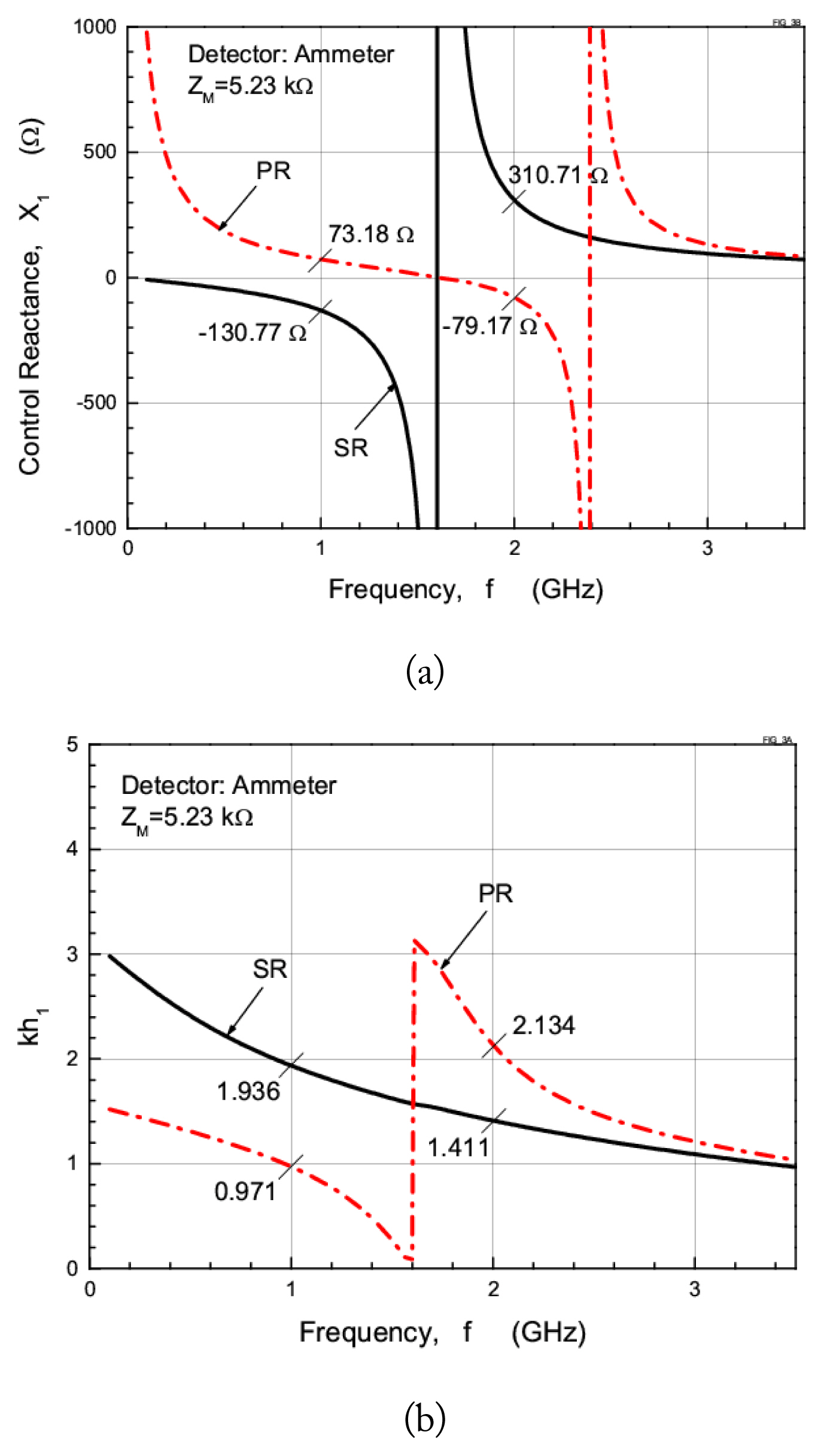
Fig. 2 shows the frequency characteristics of the length of the control element, jX1 = jZ0tan(kh1), which occurs with forced resonance from (8) when the cutoff cavity probe resonates forcefully from adjusting the control element for the ammeter (ZM = 5.23 k╬®) connection. For the ammeter connecttion at 1 GHz, SR and PR occur at kh1 = 1.936 (X1 = ŌłÆ130.77 ╬®) and kh1 = 0.971 (X1 = 73.18 ╬®), respectively. At 2 GHz, SR occurs at kh1 = 1.411 (X1 = 310.71 ╬®), and PR occurs at kh1 = 2.134 (X1 = ŌłÆ79.17 ╬®). These resonance modes are summarized in Table 2.
As shown in Fig. 2, the cutoff cavity probe generates SR or PR at given frequencies by adjusting the control element jX1 for the ammeter connection. The PR for the ammeter connection occurs at kh1 Ōēł 0 (X1 Ōēł 0 ╬®) at around 1.60 GHz, as shown in Fig. 2. The frequency of 1.60 GHz is critical for determining the resonance. The vicinity of 1.60 GHz is sensitive when obtaining the resonance by adjusting the control element and should not be in the crack detection using FRMM. The characteristics of a voltmeter connection are almost the same as those of the ammeter connection. As mentioned previously, the forced resonances other than those at 1.60 GHz are useful for crack detection by the FRMM. It is necessary to analyze the current states of the cutoff cavity probe at the resonance and around it. Knowledge of the input impedance characteristic of the cutoff cavity and the detector current (the ammeter connection point current) is needed to check the types of resonance.
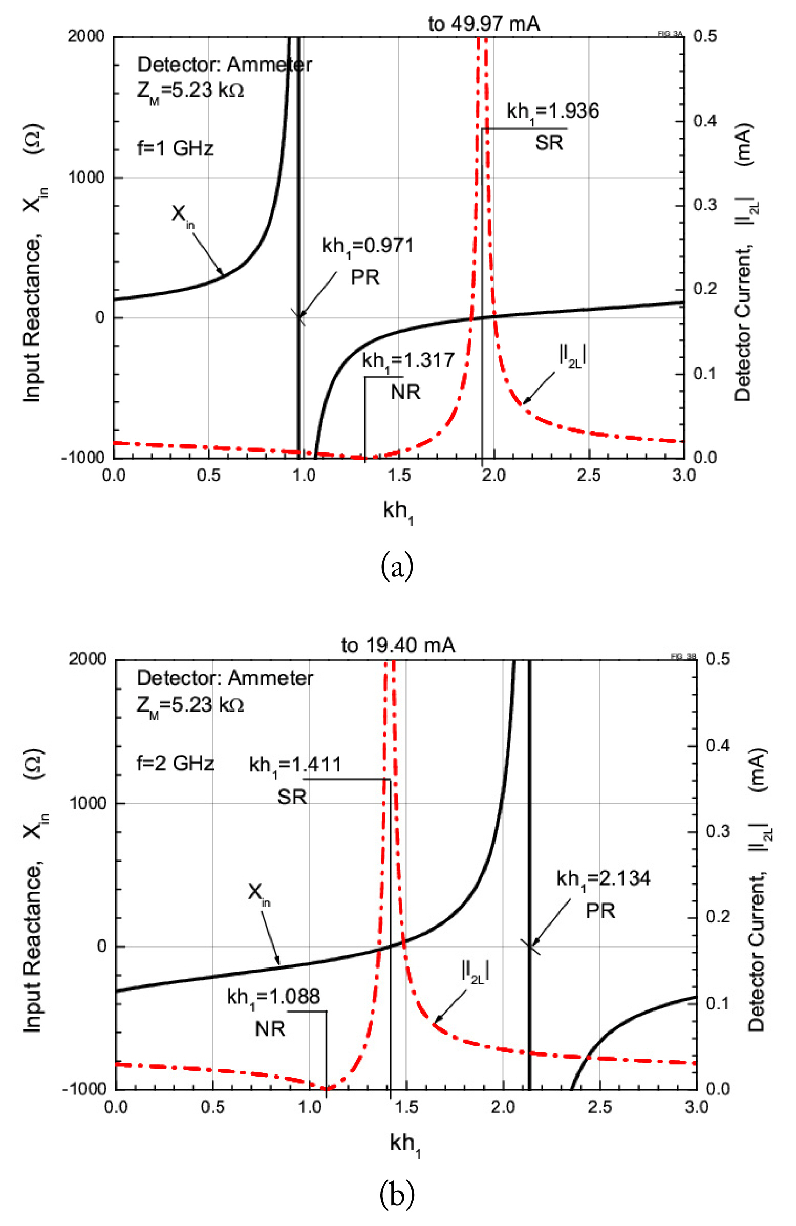
Fig. 3 shows the detector current and input reactance versus the length of the control reactance when the operating frequency is fixed at 1 GHz and 2 GHz as an example. To determine whether SR or PR is occurring, it also shows the input reactance of the cutoff cavity probe. As shown in Fig. 3(a), for the ammeter connection at 1 GHz, SR occurs when kh1 = 1.936 (X1 = ŌłÆ130.77 ╬®). The maximum current state also occurs. PR occurs when kh1 = 0.971 (X1 = 73.18 ╬®), and the current state slowly changes. The minimum current (Ōēł 0 mA) appears when kh1 = 1.317 (X1 = 192.76 ╬®), which is the NR state. For the ammeter connection at 2 GHz shown in Fig. 3(b), SR occurs when kh1 = 1.411 (X1 = 310.71 ╬®), and the input reactance, Xin, changes from capacitive to inductive. The maximum current state occurs. PR occurs when kh1 = 2.134 (X1 = ŌłÆ79.17 ╬®), and the input reactance changes from inductive to capacitive. The current state slowly changes. The detector current also appears to be minimized (Ōēł 0 mA) at kh1 = 1.088 (X1 = 95.39 ╬®), which is the NR state.
2. Classification of Current States
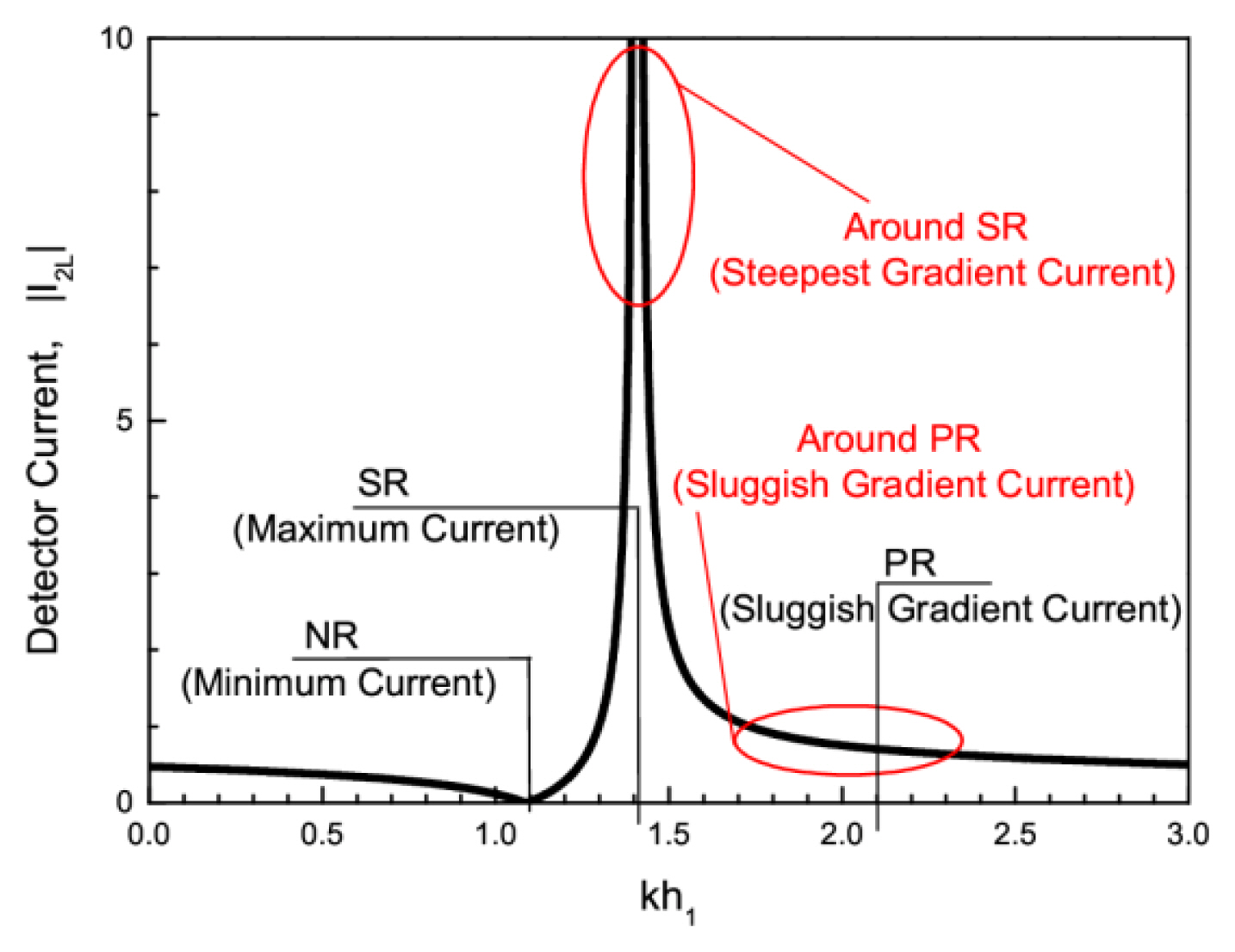
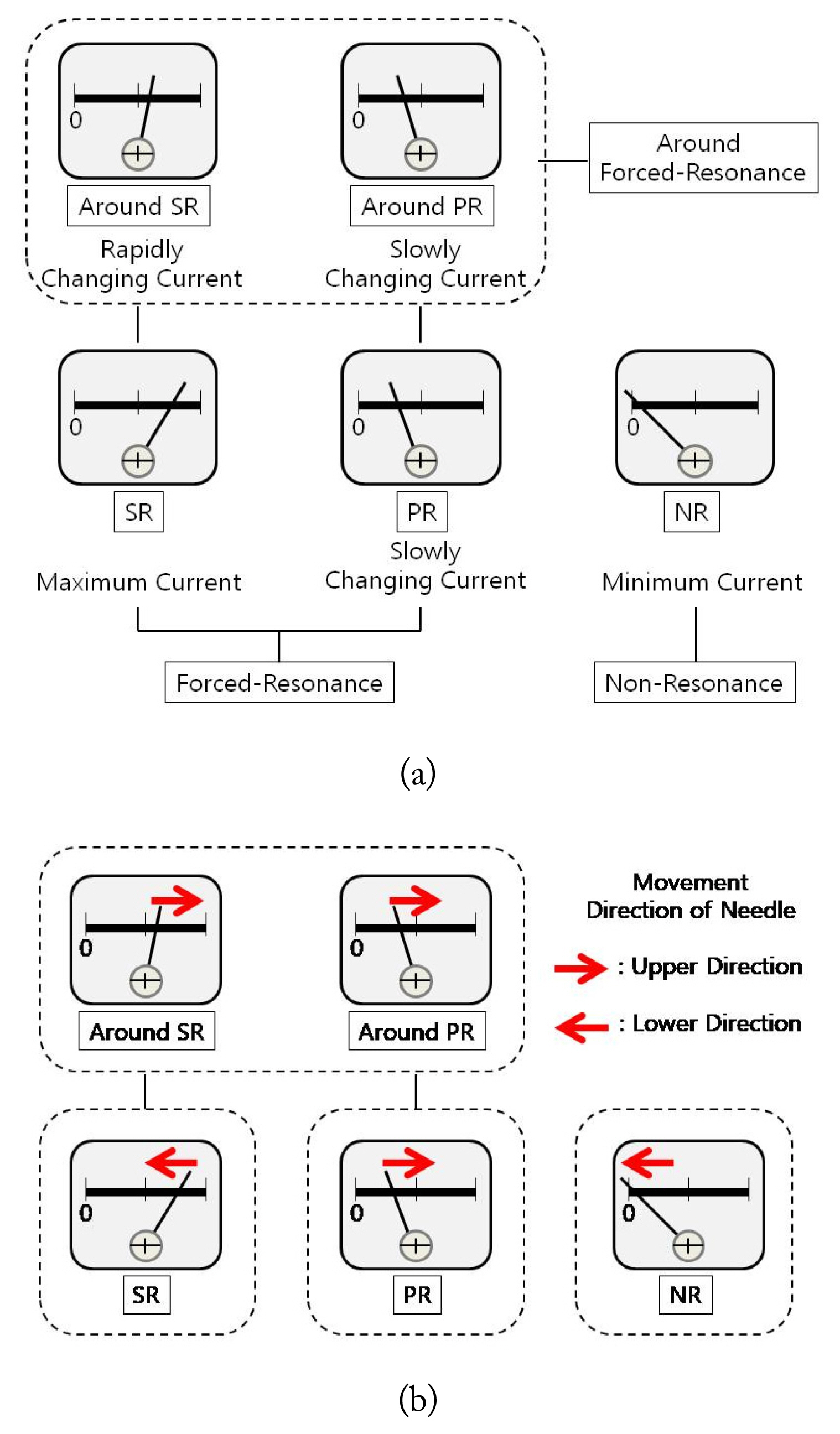
Based on the current states for the ammeter connection in Fig. 3, the current states of the cutoff cavity probe have a maximum current (at SR), minimum current (at NR), rapidly changing current (around SR), and slowly changing current (at PR and around it). These detector current states and resonant types are illustrated in Fig. 4. There are four kinds of current states: (1) SR with maximum current, (2) PR and the surrounding region, which has a slowly changing current, (3) NR with minimum current, and (4) region around the SR with a rapidly changing current. These current states are applicable to crack detection using FRMM. One of the four current states can be used for more sensitive crack detection when setting the reference current in the preparation stage. Crack signals are detected from the deviations of the reference current.
Fig. 5 shows the classification of resonant types and directions of the detector needle movement as the crack signal appears with the four current states in the crack detection stage. Fig. 5(a) shows the three types of resonance: (1) forced resonance (SR and PR), (2) NR, and (3) region around the forced resonance. As mentioned previously, SR has the maximum current, NR has the minimum current, PR and the surrounding region have a slowly changing current, and the region around the SR has a rapidly changing current, as shown in Fig. 4. For these current states, the directions of the needle movement are shown in Fig. 5(b). The needle moves in the lower or upper direction depending on the state of crack at a given frequency. The needle movement direction should be discussed in detail at the crack detection stage. However, this paper presents only one example. The needle movement directions for the crack of W = 1 mm and d = 1 mm are shown in Fig. 5(b). In this case, when the probe scans a crack in the detection stage, the needle moves in the lower directional movement if we use SR (maximum current) and NR (minimum current). For PR (slowly changing current), the needle moves in the upper direction. Using the region around SR (rapidly changing current) and around PR (slowly changing current), the needle also moves in the upper directions when the probe scans a crack. To check the needle movement shown in Fig. 5(b), the experimental results for the crack of W = 1 mm and d = 1 mm at 1 GHz are shown in Table 3. As a future study on the detection stage, more detailed research on the movement direction of the needle for various crack dimensions is needed.
As a result, using SR and the region around SR leads to the best sensitivity for crack detection, as the current changes have the steepest gradient. PR and the region around the PR can be used for crack detection, but sensitivity is lower than that of the region around the SR. Using NR is also possible, but sensitivity will be even lower. Therefore, PR and NR can also be used for crack detection, but they are not as advantageous as SR.
V. Experiments
To validate the forced resonance and non-resonance currents of the probe, the calculated resonant currents were compared with the measured currents. The cutoff cavity was made with copper using electroforming technology and plated with gold, and a coaxial sliding short (Model 1909C2 at 0.8ŌĆō4 GHz; Maury Microwave Corp., Ontario, CA, USA) was used as a control element. The dimensions of the cutoff cavity used in the experiments are a = 40 mm, b = 20 mm, c = 80 mm, s1 = 30 mm, s2 = 60 mm, t1 = t2 = a/2, and r1 = r2 = 1 mm. An NEC 1SS99 diode and ammeter (20 ╬╝A range) were connected to the parasitic post. The operating frequency used was 1 GHz, and the length of the control element was adjusted to obtain the forced resonance in the cutoff cavity.
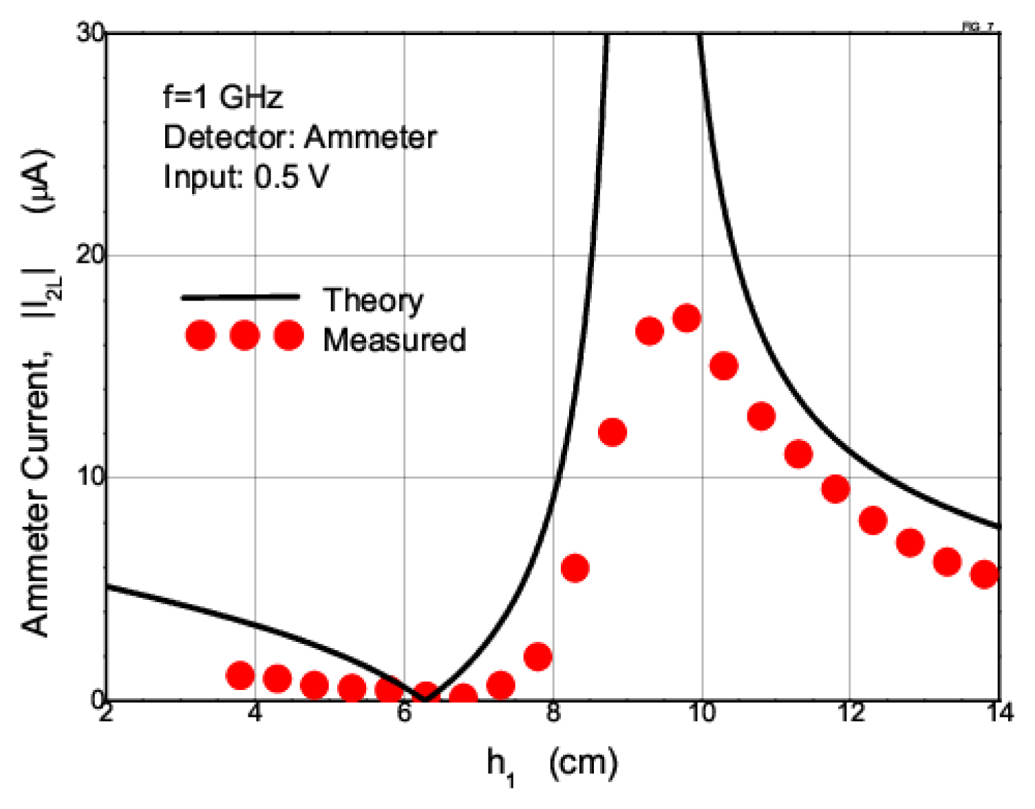
Fig. 6 shows a photograph of the manufactured cutoff cavity probe with the control element and experimental setup. Fig. 7 shows the calculated and measured resonance currents for the ammeter connection. The calculated currents showed a reasonable agreement with the experimental results. The deviation could be due to the losses of the cutoff cavity and the control element and the effect of fabrication errors.
VI. Conclusion
This study considered the forced resonance characteristics of a cutoff cavity probe that could be applied to crack detection using FRMM. There were four kinds of current states: maximum current (at the SR), minimum current (at the NR), rapidly changing current (around the SR), and slowly changing current (at the PR and around the PR). These current characteristics were classified. The SR (maximum current) and the region around SR were the most applicable current states. The NR, PR, and the region around PR are also available for crack detection, but their sensitivity is lower than that of SR and the surrounding region. The actual crack detection using these current states can be examined in future works.