J. Electromagn. Eng. Sci Search

CLOSE


J. Electromagn. Eng. Sci > Volume 20(4); 2020 > Article
Ali, Wang, Yun, Lee, and Park: Compact Slot Antenna Integrated with a Photovoltaic Cell

Abstract

This paper presents a compact low-profile slot antenna integrated with a photovoltaic cell. The photovoltaic cell consists of a top metal grid, gallium arsenide substrate, and metallic bottom contact. The metallic bottom contact was used as a ground plane where the slot was etched for resonance. A second substrate was placed under the ground plane, and a 50 Ω microstrip line was printed on its bottom side to excite the slot. A chip inductor was used as a radio frequency (RF) choke in the alternating current blocking circuit to suppress RF current leakage towards the photovoltaic cell. Hence, the proposed antenna has a unique feature of functioning simultaneously as a photovoltaic cell and an antenna. The overall dimensions––25 mm × 31.75 mm × 0.893 mm (0.48λo × 0.61λo × 0.017λo at 5.77 GHz)––of the photovoltaic cell-integrated slot antenna structure can be used effectively with Internet of Things devices.

I. Introduction

The approach of designing an antenna and a photovoltaic cell on the same substrate is useful for reducing costs. However, designing them separately is inefficient for reducing the size and weight of an Internet of Things (IoT) system. Many recent studies have explored the integration of photovoltaic cells with antennas because of the potential advantages of wireless communication. An effective approach is stacking or overlying to reduce the size and weight. The challenge in this approach is to increase sunlight exposure when the antenna is placed on top of the photovoltaic cell [14].
Several techniques, such as the use of a mesh antenna [2, 3] and transparent material [5], have been employed to increase sunlight exposure. Usually, when the antenna and photovoltaic cell are integrated, they are independent of each other [612]. In some cases, however, the photovoltaic cell is a part of the antenna and thus enhances the performance of the antenna. An aluminum layer in the solar cell is used as a ground plane for the antenna [13] to provide a reduced footprint, and the solar cell metasurfaces are used to obtain enhanced bandwidth characteristics [14, 15]. Researchers have designed state-of-the-art photovoltaic cell-integrated antennas that are large in size with complex geometries. Given the advances in the application of IoT technologies, simple and compact low-profile photovoltaic built-in antennas that can be easily attached to IoT devices are needed.
In this paper, a compact single-device photovoltaic cell-integrated antenna is proposed for IoT applications. Typically, the antenna and the photovoltaic cell are used separately, thereby occupying substantial real estate. The need for small low-profile devices that can be easily integrated into IoT devices was a consideration. The designed antenna has a low profile and small size; therefore, it can save crucial real estate when used with IoT devices. The designed photovoltaic cell-integrated antenna has 100% sunlight exposure and exhibits excellent antenna characteristics (impedance bandwidth, gain, and radiation pattern). In addition, the photovoltaic cell-integrated slot antenna has an omnidirectional radiation pattern, which is valuable for IoT applications.

II. Photovoltaic Cell-Integrated Antenna Geometry

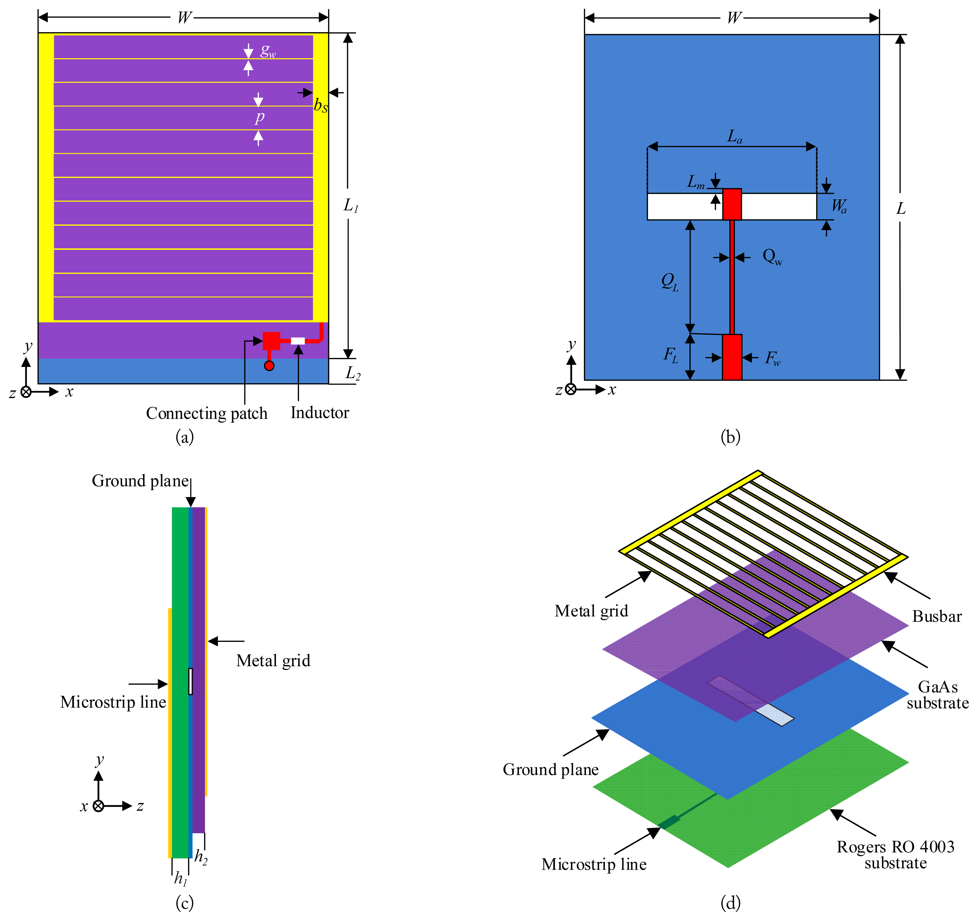
Fig. 1 shows the geometry of the photovoltaic cell-integrated slot antenna. A photovoltaic cell made of GaAs was used for integration with the slot antenna. The thickness of the GaAs layer (ɛr = 12.9 and tanδ = 0.0004) was h2 = 0.385 mm. The photovoltaic cell was configured as follows: a metal grid lined with two bus bars was printed on the top side of the GaAs layer. The grid lines were spaced at a distance of p = 1.975 mm apart. The values for the width of the grid line and bus bar were gw = 0.1 mm and bs = 1 mm, respectively. A metallic bottom contact is placed under the GaAs layer. The metallic bottom contact of the photovoltaic cell also served as a ground plane for the slot antenna. For resonance, a slot was cut in the bottom contact of the photovoltaic cell. An alternating current (AC) blocking circuit implemented with a 59 nH inductor was used to prevent the flow of radio frequency (RF) current towards the solar cell. A connecting patch was used to connect one inductor terminal to the antenna ground plane. The other inductor terminal was connected to the bus bar. Fig. 1(a), (c), and (d) show the top, side, and three-dimensional (3D) views, respectively, of the photovoltaic cell-integrated slot antenna. The detailed structure and characteristics of the photovoltaic cells used in this work were presented in [16] and [17].
Fig. 1(b) illustrates the detailed geometry of the slot antenna, which comprises a microstrip feedline, substrate, and ground plane. A simple slot structure was used so that there would be a minimal effect on the performance of the photovoltaic cell. Moreover, slot antennas are smaller in size, low profile, and they can be easily integrated into planar and/or non-planar surfaces. To design the slot antenna, a Rogers RO4003 substrate with a dielectric constant of ɛr = 3.38 and a loss tangent of tanδ = 0.0027 was used. The size of the substrate was L × W and a thickness of 0.508 mm. The metallic bottom contact for the photovoltaic cell, which had a slot size of La × Wa, was also used as the ground plane. The dimensions of the slot controlled the resonance frequency of the slot antenna. A 50 Ω microstrip feedline was placed under the substrate to excite the slot. A quarter-wavelength transformer with a size of QL × Qw was introduced between the slot and the microstrip feedline to improve impedance matching. The designed photovoltaic cell-integrated slot antenna was simulated with an ANSYS high-frequency structure simulator. The final parameter values for the designed photovoltaic cell-integrated slot antenna are as follows: h1 = 0.508 mm, h2 = 0.385 mm, W = 25 mm, L = 31.75 mm, L1 = 29.5 mm, L2 = 2.25 mm, La = 12.5 mm, Wa = 2.1 mm, Qw = 0.25 mm, QL = 11.7 mm, Fw = 1.3 mm, FL = 4.25 mm, and Lm = 0.25 mm.

III. Measured and Simulated Results

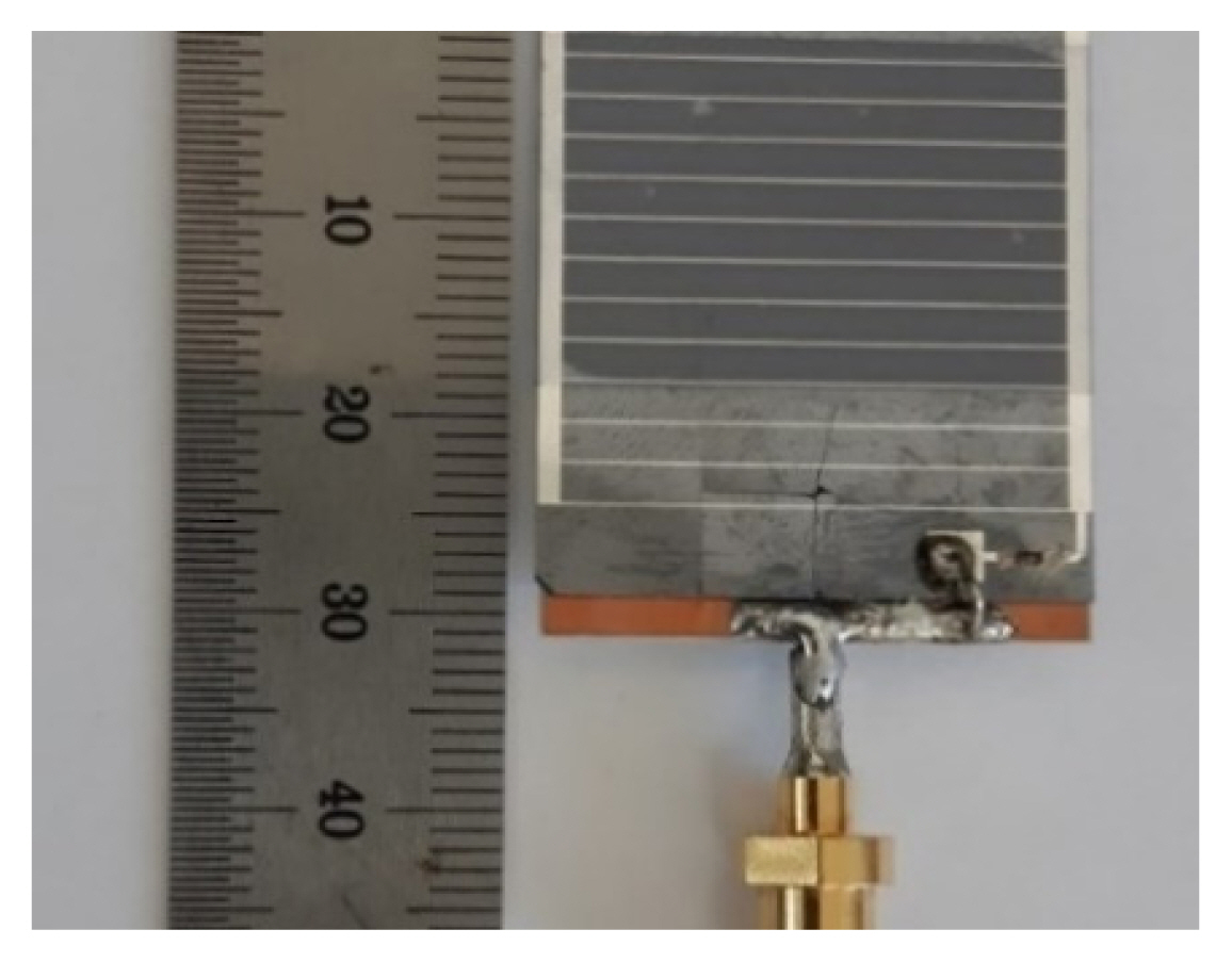
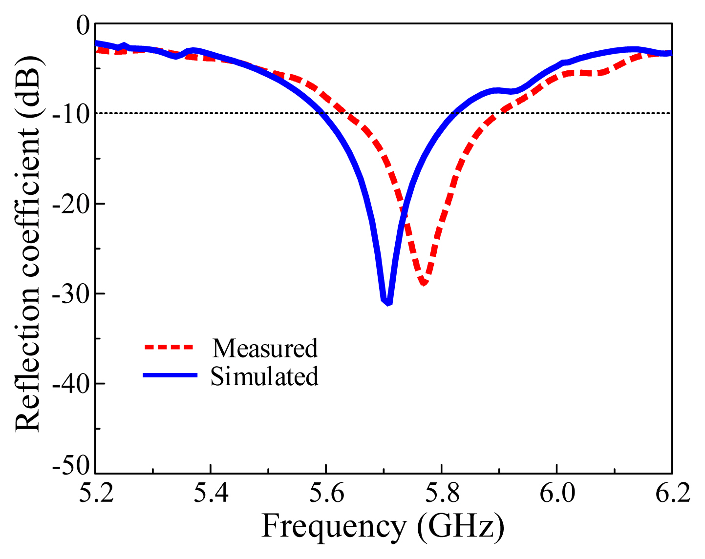
A prototype of the proposed photovoltaic cell slot-integrated antenna was fabricated and measured to verify the simulation results regarding the reflection coefficient and radiation properties. A photograph of the fabricated prototype is presented in Fig. 2. The reflection coefficient of the fabricated photovoltaic cell slot integrated antenna was measured with a R&S ZVA67 network analyzer (Rohde and Schwarz, Munchen, Germany). The measured and simulated reflection coefficients are presented in Fig. 3. The figure indicates that acceptable agreement was found between the simulated and measured reflection coefficients. The measured impedance bandwidth of the fabricated pro-totype was 270 MHz, from 5.63 GHz to 5.9 GHz, with an increase of 40 MHz as compared to a simulation result that was 230 MHz, from 5.59 GHz to 5.82 GHz.
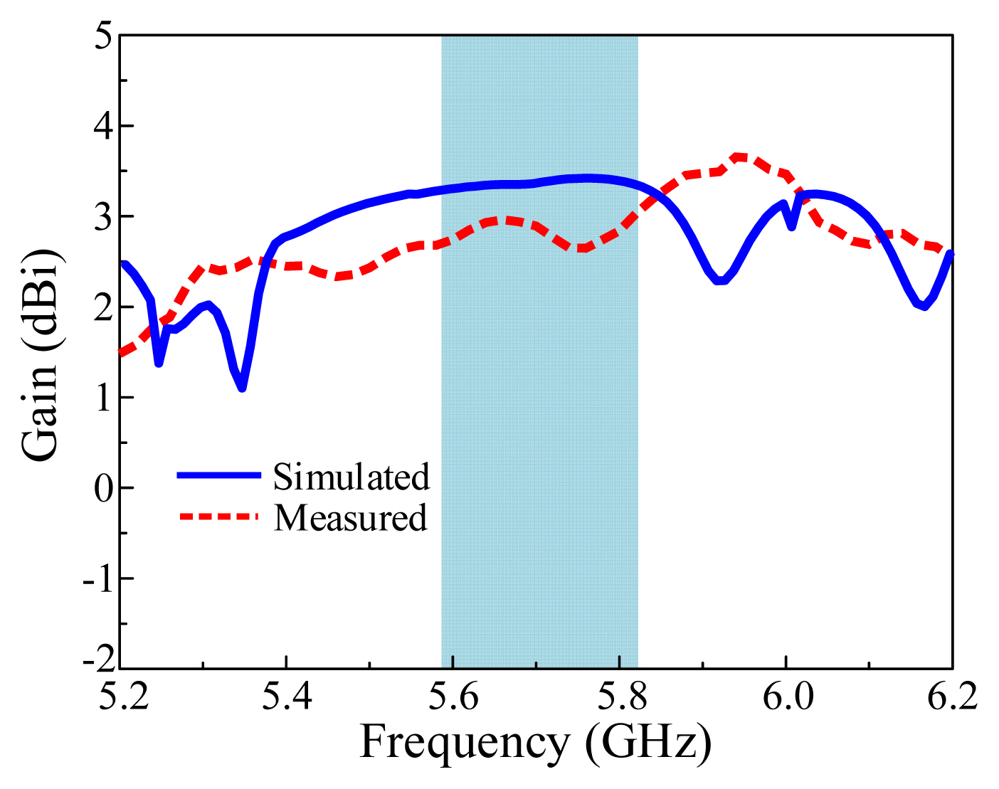
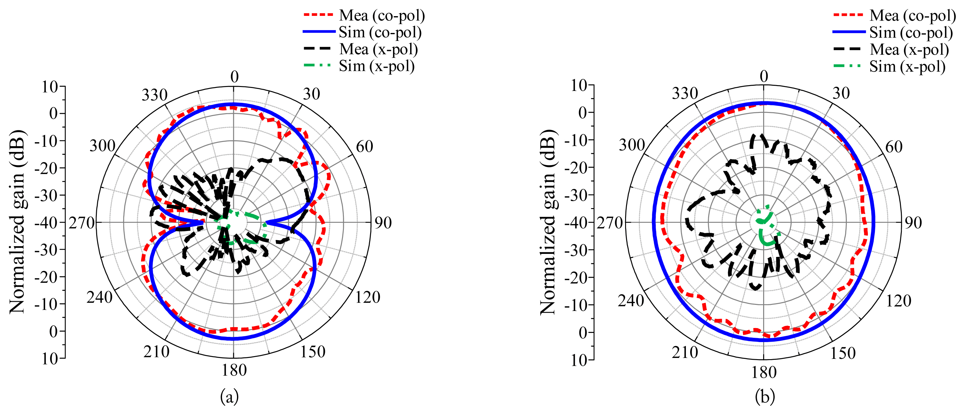
The measured and simulated gain values are illustrated in Fig. 4. The maximum simulated gain was 3.41 dBi; however, it fell slightly to a maximum of 3 dBi within the impedance bandwidth. This reduction could be attributed to the measurement setup; thus, it is more likely to have been a measurement error. The designed photovoltaic cell-integrated slot antenna has a dipole-like omnidirectional radiation pattern. Its radiation characteristics did not change in the presence or absence of the photovoltaic cell. The radiation characteristics were measured in a full anechoic chamber at the RFID/USN Center, Incheon, Republic of Korea. The size of the full anechoic chamber was 15.2 m (W) × 7.9 m (L) × 7.9 m (H). A horn antenna was used as a transmitter, and the fabricated photovoltaic cell antenna was used as a receiver. The transmitter and receiver were separated by a distance of 10 m. The photovoltaic cell antenna was moved circularly from −180° to 180° while the horn antenna was fixed. The measured and simulated radiation patterns of the designed photovoltaic cell-integrated slot antenna at 5.70 GHz are shown in Fig. 5. The illustration reveals that the measured and simulated radiation patterns were in relatively good agreement in both the E- and H-planes. The measured results showed that there were some fluctuations in both planes. These fluctuations could have resulted from using tape and foam rack in the measurement setup. A performance comparison of the proposed photovoltaic cell antenna with other designs is presented in Table 1.

IV. Conclusion

A compact low-profile photovoltaic cell-integrated slot antenna has been presented for IoT applications. The metallic bottom contact of the photovoltaic cell was used as a ground plane for the antenna, and a slot was etched on it for resonance. An AC blocking circuit was used to limit the RF current flow towards the solar cell. Therefore, the proposed photovoltaic cell-integrated slot antenna can function simultaneously as an antenna and a photovoltaic cell. In addition, the antenna exhibited excellent gain performance and a stable omnidirectional radiation pattern within the impedance bandwidth. The low profile, compact size, 100% exposure to light, and good performance of the proposed antenna make it suitable for use as an on-board power source for low-power IoT applications and sensor technologies.

Acknowledgments

This work was supported in part by the National Research Foundation (NRF) of Korea grant funded by the Korean government (MSIT) (No. 2018R1D1A1A02086071); in part by the “Human Resources Program in Energy Technology” of the Korea Institute of Energy Technology Evaluation and Planning (KETEP)-granted financial resources from the Ministry of Trade Industry & Energy, Republic of Korea (Project No. 20184030292220); and in part by the Ajou University research fund.

Fig. 1
Antenna geometry: (a) top view, (b) ground plane with a slot and a feed line, (c) side view, and (d) three-dimensional view.
jees-2020-20-4-248f1.jpg
Fig. 2
Fabricated prototype.
jees-2020-20-4-248f2.jpg
Fig. 3
Measured and simulated reflection coefficients.
jees-2020-20-4-248f3.jpg
Fig. 4
Measured and simulated gain.
jees-2020-20-4-248f4.jpg
Fig. 5
Measured and simulated radiation patterns at 5.70 GHz: (a) E-plane and (b) H-plane.
jees-2020-20-4-248f5.jpg
Table 1
Performance comparison of proposed and other photovoltaic cell antennas
[1] [2] [4] [18] [19] Proposed
Size (λ03) 1.27 × 1.27 × 0.056 0.62 × 1.03 × 0.06 0.60 × 0.72 × 0.34 1.19 × 1.15 × 0.067 1.10 × 1.10 × 0.076 0.48 × 0.61 × 0.017
BW (%) 3.35 4 4.3
3.5
4.32 4 4.6
OT (%) 94.7 70 87 100 100 100
Gain (dBi) 3.5 3a 6.05
7.61
7.8 4.1a 3
Rad. type Uni Uni Uni Uni Omni Omni

OT=optical transparency.

a Realize gain.

References

1. O O’Conchubhair, P McEvoy, and MJ Ammann, "Integration of antenna array with multi crystalline silicon solar cell," IEEE Antennas and Wireless Propagation Letters, vol. 14, pp. 1231–1234, 2015.
crossref
2. SK Podilchak, D Comite, BK Montgomery, Y Li, VGG Buendia, and YMM Antar, "Solar-panel integrated circularly polarized meshed patch for CubeSats and other small satellites," IEEE Access, vol. 7, pp. 96560–96566, 2019.
crossref
3. TW Turpin and R Baktur, "Meshed patch antennas integrated on solar cells," IEEE Antennas and Wireless Propagation Letters, vol. 8, pp. 693–696, 2009.
crossref
4. F Nashad, S Foti, D Smith, M Elsdon, and O Yurduseven, "Ku-band suspended meshed patch antenna integrated with solar cells for remote area applications," Progress in Electromagnetics Research C, vol. 83, pp. 245–254, 2018.
crossref
5. S Zarbakhsh, M Akbari, M Farahani, A Ghayekhloo, TA Denidni, and AR Sebak, "Optically transparent sub-array antenna based on solar panel for CubeSat application," IEEE Transactions on Antennas and Propagation, vol. 69, no. 1, pp. 319–328, 2020.
crossref
6. O Yurduseven and D Smith, "A solar cell stacked multi-slot quad-band PIFA for GSM, WLAN and WiMAX networks," IEEE Microwave and Wireless Component Letters, vol. 23, no. 6, pp. 285–287, 2013.
crossref
7. Y Zhang, S Shen, CY Chiu, and R Murch, "Hybrid RF-solar energy harvesting systems utilizing transparent multiport micromeshed antennas," IEEE Transactions on Microwave Theory and Techniques, vol. 67, no. 11, pp. 4534–4546, 2019.
crossref
8. R Caso, A D’Alessandro, A Michel, and P Nepa, "Integration of slot antennas in commercial photovoltaic panels for stand-alone communication systems," IEEE Transactions on Antennas and Propagation, vol. 61, no. 1, pp. 62–69, 2012.
crossref
9. O Yurduseven, D Smith, N Pearsall, and I Forbes, "A solar cell stacked slot-loaded suspended microstrip patch antenna with multiband resonance characteristics for WLAN and WiMAX systems," Progress in Electromagnetics Research, vol. 142, pp. 321–332, 2013.
crossref
10. T Yekan and R Baktur, "Conformal integrated solar panel antennas: two effective integration methods of antennas with solar cells," IEEE Antennas and Propagation Magazine, vol. 59, no. 2, pp. 69–78, 2017.
crossref
11. EH Lim, KW Leung, CC Su, and HY Wong, "Green antenna for solar energy collection," IEEE Antennas and Wireless Propagation Letters, vol. 9, pp. 689–692, 2010.
crossref
12. Y Al-Adhami and E Ercelebi, "Plasmonic metamaterial dipole antenna array circuitry based on flexible solar cell panel for self-powered wireless systems," Microwave and Optical Technology Letters, vol. 59, no. 9, pp. 2365–2371, 2017.
crossref
13. SV Shynu, MJR Ons, P McEvoy, MJ Ammann, SJ McCormack, and B Norton, "Integration of microstrip patch antenna with polycrystalline silicon solar cell," IEEE Transactions on Antennas and Propagation, vol. 57, no. 12, pp. 3969–3972, 2009.
crossref
14. SX Ta and I Park, "A circularly polarized antenna integrated with a solar cell metasurface for CubeSat," In: Proceedings of 2018 Asia-Pacific Microwave Conference (APMC); Kyoto, Japan. 2018, pp 696–698.
crossref
15. SX Ta and I Park, "A circularly polarized antenna integrated with metasurface solar cells," In: Proceedings of 2017 IEEE-APS Topical Conference on Antennas and Propagation in Wireless Communications (APWC); Verona, Italy. 2017, pp 120–122.
crossref
16. SX Ta, JJ Lee, and I Park, "Solar-cell metasurface-integrated circularly polarized antenna with 100% insolation," IEEE Antennas and Wireless Propagation Letters, vol. 16, pp. 2675–2678, 2017.
crossref
17. S Moon, K Kim, Y Kim, J Heo, and J Lee, "Highly efficient single-junction GaAs thin-film solar cell on flexible substrate," Scientific Reports, vol. 6, article no. 30107, 2016.
crossref pmid pmc pdf
18. O Yurduseven and D Smith, "Solar cell stacked dual-polarised patch antenna for 5.8 GHz band WiMAX network," Electronics Letters, vol. 49, no. 24, pp. 1514–1515, 2013.
crossref
19. S Liu, D Yang, Y Chen, X Zhang, and Y Xiang, "Compatible integration of circularly polarized omnidirectional metasurface antenna with solar cells," IEEE Transactions on Antennas and Propagation, vol. 68, no. 5, pp. 4155–4160, 2020.
crossref

Biography

jees-2020-20-4-248f6.jpg
Ahmed Ali received an M.S. degree in electrical engineering with a specialization in telecommunication engineering from COMSATS University Islamabad, Attock, Pakistan in 2019. He is currently pursuing a Ph.D. degree in the Department of Electrical and Computer Engineering at Ajou University, Suwon, Republic of Korea. His current research interests include developing metasurface antennas and photovoltaic cell-integrated antennas for IoT applications.

Biography

jees-2020-20-4-248f7.jpg
Heesu Wang received B.S. and M.S. degrees in electrical and computer engineering from Ajou University, Suwon, Republic of Korea, in 2018 and 2020, respectively. He is currently studying for his Ph.D. degree in the Department of Electrical and Computer Engineering at Ajou University. His research interests include the design of patch antennas, printed antennas, small antennas, and metasurface antennas for wireless communication applications.

Biography

jees-2020-20-4-248f8.jpg
Yeojun Yun received a B.S. degree in electrical and computer engineering from Ajou University, Suwon, Republic of Korea, in 2014. He is currently studying for his Ph.D. degree in the Department of Electrical and Computer Engineering at Ajou University. His research interests include the design of flexible III–V photovoltaic cells, high-quality periodic nanostructures, and fabrication processes for flexible optoelectronic nanodevices.

Biography

jees-2020-20-4-248f9.jpg
Jaejin Lee received B.S. and M.S. degrees in physics education from Seoul National University, Republic of Korea, and a Ph.D. degree in electrical engineering from the Northwestern University, USA. He is currently a professor in the Department of Electrical and Computer Engineering at Ajou University, Suwon, Republic of Korea. He was a visiting scholar in the Department of Electrical and Computer Engineering at the University of Wisconsin at Madison, USA. His research interests include the metalorganic chemical vapor deposition (MOCVD) growth of III–V compound semiconductor heterostructures, high-efficiency III–V solar cells, LEDs, and semiconductor diode lasers. He has authored and co-authored more than 100 refereed journal articles and conference papers. He holds more than 20 patents.

Biography

jees-2020-20-4-248f10.jpg
Ikmo Park received a B.S. degree in electrical engineering from the State University of New York at Stony Brook, and M.S. and Ph.D. degrees in electrical engineering from the University of Illinois at Urbana–Champaign. He joined the Department of Electrical and Computer Engineering at Ajou University in 1996. He previously worked at the Device & Materials Laboratory at the LG Corporate Institute of Technology, Seoul, Republic of Korea, where he was engaged in the research and development of antennas for personal communication systems, wireless local area networks, and direct broadcasting systems. He has authored and co-authored more than 300 technical journal articles and conference papers. He holds more than 40 domestic and international patents. He is a member of the board of directors of the Korea Institute of Electromagnetic Engineering and Science (KIEES). He is a member of the editorial boards of the International Journal of Antennas and Propagation and MDPI’s Electronics and an associate editor of IET’s Electronics Letters. He serves as chair, organizer, and member of the program committees for several conferences, workshops, and short courses related to electromagnetics. His current research interests include the design and analysis of microwave, millimeter-wave, terahertz-wave, and nano-structured antennas.

ABOUT
ARTICLE CATEGORY

Browse all articles >

BROWSE ARTICLES
AUTHOR INFORMATION
Editorial Office
#706 Totoo Valley, 217 Saechang-ro, Yongsan-gu, Seoul 04376, Korea
Tel: +82-2-337-9666    Fax: +82-2-6390-7550    E-mail: admin-jees@kiees.or.kr                

Copyright © 2024 by The Korean Institute of Electromagnetic Engineering and Science.

Developed in M2PI

Close layer
prev next