


I. Introduction
In recent years, omnidirectional array antennas with the following characteristics have become necessary for wireless communication systems: (1) wide bandwidth to cover various frequency bands, (2) dual polarization for durable communication in complex environments, and (3) low gain variation in the horizontal plane for omnidirectional coverage [1, 2]. Various omnidirectional antennas satisfying the above characteristics have been reported. Most of these antennas have dual polarizations and low gain variations in the horizontal plane. However, their bandwidths are quite limited, reaching only 25% [3] or 30% [4]. Antennas with an extended bandwidth in the vertical polarization of over 110% have been proposed [5ŌĆō7], but their bandwidths in the horizontal polarization are still limited to below 65%.
The tightly coupled dipole array (TCDA) proposed by Munk [8] can achieve ultra-wideband because of the compensation between the coupling capacitance of the neighboring dipole antennas and the inductance of the ground plane at low frequencies. Various types of dual-polarized TCDAs with very broad bandwidths have been introduced, for example, 5:1 [9], 3:1 [10], 7.35:1 [11], and 6:1 [12]. In developing various TCDA radiation patterns, a one-dimensional TCDA with a fan-shaped beam has also been presented [13, 14]. However, studies on TCDA antennas have been limited to planar arrays for achieving pencil or fan beams.
In this study, we propose a cylindrical TCDA (C-TCDA) design for an omnidirectional radiation pattern, which has a wide bandwidth and dual polarization compared with conventional omnidirectional antennas. In Section II, we analyze the proposed C-TCDA and verify that it has similar impedance characteristics to planar TCDAs. The dual-polarized omnidirectional TCDA antenna design and its performances are introduced in Section III. The conclusions are presented in Section IV.
II. Theory of the C-TCDA
In this section, the equations for the C-TCDA and its equivalent circuit are presented. We approach the C-TCDA analysis in a similar manner as the analysis of a planar TCDA. The cylindrical coordinates (Žü, Žå, z) are used, with the cylinder being parallel to the z-axis and the direction of wave propagation being along the Žü-axis. Two types of C-TCDA with elements arranged in the Žå-direction (horizontal polarization) and the z-direction (vertical polarization) are analytically solved. The cylindrical and planar TCDAs are then compared.
1. Horizontally Polarized C-TCDA
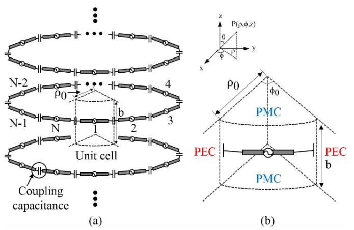
A schematic of the horizontally polarized C-TCDA is shown in Fig. 1(a). The horizontally polarized N elements of the TCDA are arranged in the Žå-direction with a period of Žå
0 = 2ŽĆ/N and repeated in the z-direction with a period of b. According to WheelerŌĆÖs current sheet array theory, a two-dimensionally periodic dipole array located in a plane can be equated to a unit dipole in a hypothetical wave-guide that has a perfect electric conductor (PEC) and a perfect magnetic conductor (PMC) boundary conditions [15]. Similar to a planar array in Fig. 1(a), the cylindrically infinite dipole array is equivalent to the unit dipole inside the hypothetical waveguide, as shown in Fig. 1(b). We assume that the medium inside the waveguide is filled with an isotropic, homogeneous, and lossless dielectric material with a permittivity ╔ø and permeability ╬╝
0. The boundaries parallel to the z-axis are PEC, and the other boundaries orthogonal to the z-axis are PMC. Therefore, the boundary conditions are written as
The field components inside the waveguide can be obtained by solving the Helmholtz wave equation using the separation-of-variables technique [15]. The current of the dipole flows in the Žå-direction, and thus the magnetic wave modes transverse to the Žå-direction exist. For the magnetic modes transverse to Žå that propagate only in the +Žü-direction (radiation direction), the vector potential satisfying the boundary conditions in Eqs. (1) and (2) can be written as
with
where p = 0, 1, 2, ŌĆ” and m = 0, 1, 2, ŌĆ”. The variable B
pm
is the coefficient of the pm mode. The wave number, k, is given by
Therefore, the fundamental mode is TM00 transverse to Žå, and the corresponding vector potential is
The field components of the dominant mode are obtained by substituting Eq. (5) into the Maxwell equations. The results are as follows:
Only E
Žå and H
z exist, signifying that the mode is TEM to the Žü mode. As E
Žå and H
z are functions of Žü, the hypothetical waveguide can be regarded as a transmission line with characteristic impedance as a function of Žü. The characteristic impedance of the transmission line for the horizontal polarization is given by
The phase constant for the TM00 mode is given by [12]
The cutoff frequencies of the pm mode is given by
The grating lobe occurs over the first cutoff frequency (m = 1) when scanning in the ╬Ė-direction because b Ōēź ╬╗/2. All modes where p > 0 and m = 0 are possible, but we focus on only the dominant mode for simplicity.
The equivalent circuit of the C-TCDA unit cell with a ground plane and a superstrate is shown in Fig. 2. Let the distances between the center of the cylinder and the ground plane, the dipole antenna, and the top of the superstrate be Žü
g, Žü
ant, and Žü
sup, respectively. The variables Z
0h and Z
suph are the characteristic impedance of free space and the superstrate for the horizontal polarization, respectively, and they are obtained by substituting the vacuum permittivity, ╔ø
0, and the superstrate permittivity, ╔ø
sup, for ╔ø in Eq. (13). The variables ╬▓
0 and ╬▓
sup are the phase constant of free space and the superstrate, respectively, which are obtained by substituting ╔ø
0 and ╔ø
sup for ╔ø in Eq. (14). The embedding impedances Z
u and Z
d are the impedances toward the outward direction and inward direction in the dipole antenna, respectively. Z
ant is the antenna impedance, which is composed of the dipole inductance, L
dipole, and the coupling capacitance, C
coupling. Therefore, the input impedance is given by Z
in = Z
ant + Z
u // Z
d = jŽē L
dipole + 1 / jŽē C
coupling + Z
u // Z
d.
2. Vertically Polarized C-TCDA
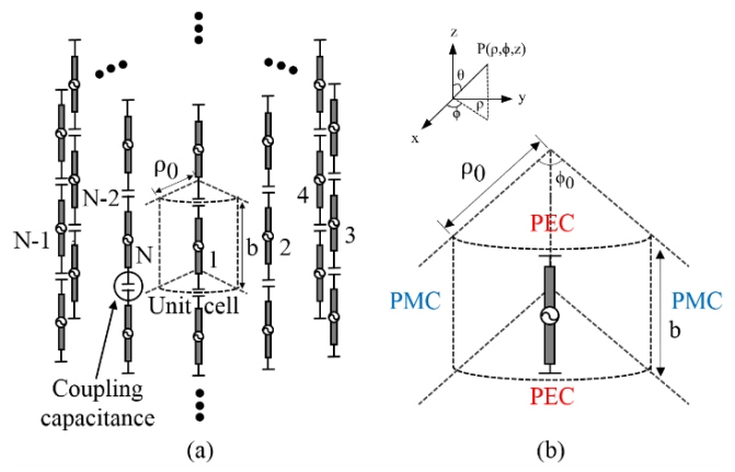
A schematic of the vertically polarized C-TCDA is shown in Fig. 3(a). The vertically polarized N elements of the TCDA are arranged in the Žå-direction with a period of Žå
0 = 2ŽĆ/N and repeated in the z-direction with a period of b. Similar to the horizontally polarized C-TCDA, the arrays are equivalent to a unit dipole existing in the hypothetical waveguide with PEC and PMC boundary conditions, as shown in Fig. 3(b). We also assume that the medium inside the waveguide is filled with an isotropic, homogeneous, and lossless dielectric material, with permittivity ╔ø and permeability ╬╝
0. Contrary to the horizontal polarization case, the boundaries parallel to the z-axis are PMC, and the other boundaries orthogonal to the z-axis are PEC. Thus, the boundary conditions are written as
The field components inside the waveguide can be obtained in a similar way to that in the horizontal polarization. The current of the dipole flows in the z-direction, and therefore the modes transverse to the z-axis exist. For the modes transverse to the z-direction that propagate only in the +Žü-direction (radiation direction), the vector potential satisfying the boundary conditions in Eqs. (16) and (17) can be written as
with k
Žü given in Eq. (4), where p = 0, 1, 2, ŌĆ”, and m = 0, 1, 2, ŌĆ”. C
pm
is the coefficient of the pm mode. The wave number, k, is given in Eq. (5). Thus, the fundamental mode is TM00 transverse to z, and the corresponding vector potential is
The field components of the dominant mode are obtained from substituting Eq. (19) into the Maxwell equations. The
results are as follows:
Only E
z
and H
Žå exist, signifying that the mode is TEM transverse to Žü. Furthermore, because E
z and H
Žå are functions of Žü, the hypothetical waveguide can be regarded as a transmission line, the characteristic impedance of which is a function of Žü. The characteristic impedance of the transmission line for the vertical polarization is
The phase constant for the TM00 mode and the cutoff frequencies of the pm mode are the same as those for the horizontal polarization given in Eqs. (14) and (15), respectively. The grating lobe occurs at the first cutoff frequency (m = 1) when scanning in the ╬Ė-direction, as b Ōēź ╬╗/2. All modes where p > 0 and m = 0 are possible, but we consider only the dominant mode for simplicity.
The equivalent circuit of the TCDA unit cell with a ground plane and a superstrate is shown in Fig. 2. Z
0v and Z
supv are the characteristic impedance of free space and the superstrate for the vertical polarization, respectively, and they are obtained by substituting ╔ø
0 and ╔ø
sup for ╔ø in Eq. (26). The variables ╬▓
0, ╬▓
sup, Z
u, Z
d, Z
ant, and Z
in are identical to those of the horizontally polarized C-TCDA.
3. Comparison with the Planar TCDA
The equivalent circuit of the planar TCDA proposed in [10] is shown in Fig. 4. Let a and d be the lengths of the hypothetical waveguide of the planar TCDA unit cell that are parallel and orthogonal to the dipole direction, respectively. The characteristic impedance of the waveguide as given by [11] is
and the wave number k is given in Eq. (5). The distance between the ground plane and the antenna is h
ant and that between the antenna and the superstrate is h
sup. Z
op and Z
supp are obtained by substituting ╔ø
0 and ╔ø
sup, respectively, for ╔ø in Eq. (17). The variables k
o and k
supp are obtained by substituting ╔ø
0 and ╔ø
sup, respectively, for ╔ø in Eq. (5).
The planar TCDA can have a wide bandwidth because the input impedance, Z
in = Z
ant + Z
up // Z
dp, is matched for a wide range of frequencies. Z
ant is determined by the dipole antenna shape and the gap size between the neighboring dipoles. However, the embedding impedance, Z
u // Z
d or Z
up // Z
dp, is inherently determined by the shape of the array structure.
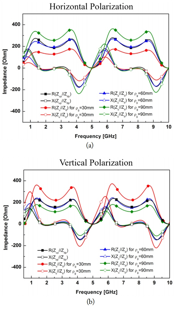
A comparison between Z
u // Z
d and Z
up // Z
dp for both polarizations is presented in Fig. 5. For the C-TCDA, the relative distances Žü
ant ŌĆō Žü
g and Žü
sup ŌĆō Žü
ant are fixed to 30 mm and 20 mm, respectively. Then, Z
u // Z
d is plotted for Žü
g = 30, 60, and 90 mm. The other specific values are ╔ø
sup = 2.2 ├Ś ╔ø
0, Žå
0 = ŽĆ/4 (N = 8), and b = 65 mm. For the planar TCDA, h
ant = Žü
ant ŌĆō Žü
g = 30 mm, h
sup = Žü
sup ŌĆō Žü
ant = 20 mm, and ╔ø
sup = 2.2 ├Ś ╔ø
0 are commonly used. The lengths of the hypothetical waveguide are chosen as a = 60 mm ├Ś Žå
0 Ōēł 70.7 mm and d = 65 mm for the horizontal polarization and a = 65 mm and d = 60 mm ├Ś Žå
0 Ōēł 70.7 mm for the vertical polarization. As a result, Z
u // Z
d when Žü
g = 60 mm and Z
up // Z
dp have similar values for both polarizations. Furthermore, when Žü
g increases, the amplitude of Z
u // Z
d increases for the horizontal polarization and decreases for the vertical polarization. As the C-TCDA has similar impedance characteristics to the planar TCDA, the C-TCDA can achieve a wide bandwidth as the planar TCDA by adjusting the antenna impedance.
III. Design of Dual-Polarized C-TCDA
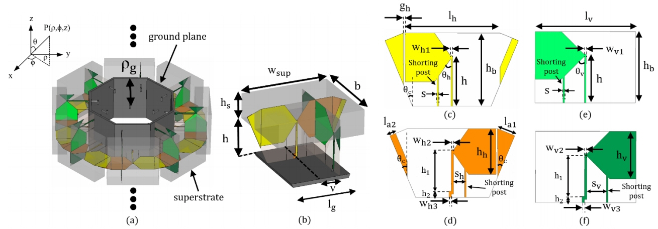
In the previous section, we verified that the C-TCDA antennas have similar impedance characteristics to the planar TCDA antenna. In this section, a dual-polarized C-TCDA antenna design and its performances are presented. For simplicity of the design, the cylinder is approximated as an octagon.
1. Design
The proposed dual-polarized C-TCDA is presented in Fig. 6. Fig. 6(a) shows a layer of the array antenna, which consists of 8 unit cells (N = 8) and has a periodic boundary in the z-direction. A unit cell of the C-TCDA antenna is illustrated in Fig. 6(b). Printed circuit boards (PCBs), which are the horizontal and vertical polarization antennas, are orthogonally soldered to the ground plane. The vertical polarization dipole antenna is located away from the center of the unit cell ground plane for low coupling between both polarizations. The substrate of both polarization antennas is designed using the Rogers RT/Duroid 5880 PCB with a substrate thickness of 0.508 mm, dielectric constant of 2.2, and dielectric loss tangent of 0.001. The superstrate is implemented by polytetrafluoroethylene (PTFE) with a dielectric constant of 2.1 and a dielectric loss tangent of 0.0005. The superstrate is used for impedance matching in a low-profile array antenna [8]. The front and back sides of the horizontal polarization dipole are presented in Fig. 6(c) and (d), and the front and back sides of the vertical polarization dipole are presented in Figs. 6(e) and (f), respectively. The feeding line of the front side of both dipoles is connected to an subminiature version A (SMA) connector and that of the back side of both dipoles is connected with the ground plane (unbalanced feeding). Both dipoles, except the feeding line, are rotationally symmetric and have shorting posts connected with the ground plane to adjust the common mode resonance frequency analyzed in [9]. The specific values are as follows: Žü
g = 60 mm, h = 30 mm, h
s = 20 mm, w
sup = 70 mm, b = 65 mm, l
g = 50 mm, v = 15 mm, l
h = 58.7 mm, g
h = 0.15 mm, l
a1 = 12.14 mm, l
a2 = 2 mm, w
h1 = 1 mm, w
h2 = w
h3 = 1.5 mm, h
h = 30 mm, s
h = 7.7 mm, ╬Ė
h = 35┬░, ╬Ė
c = 22.5┬░, l
v = 63 mm, w
v1 = w
v2 = w
v3 = 1 mm, h
v = 30 mm, s
v = 12.7 mm, ╬Ė
v = 45┬░, s = 0.1 mm, h
b = 45 mm, h
1 = 26 mm, and h
2 = 4 mm. The C-TCDA was simulated by CST Microwave Studio.
2. Performance
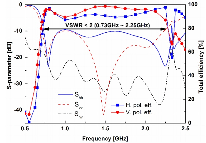
Fig. 7 shows the simulated voltage standing wave ratio (VSWR) and total efficiency for the C-TCDA antenna. The overlapped bandwidth is 3.08:1 (from 0.73 GHz to 2.25 GHz) with VSWR less than 2. The coupling between the horizontal and vertical polarizations is under 18 dB, and the total efficiency, including return loss and radiation efficiency, is over 86% for both polarizations in the frequency band.
A phase difference between neighboring layers is necessary to scan in the ╬Ė-direction while maintaining the omnidirectional pattern. Let the phase difference ╬ö ╬Ė be given by
where ╬Ė
s is the desired scan angle. Fig. 8 shows the VSWR versus the frequency graphs for ╬ö ╬Ė = 29.25┬░, 50┬░, 70┬░, and 87.75┬░. If |╬Ė
s| Ōēź 30┬░, f Ōēź c╬ö ╬Ė/ŽĆb, as obtained from the modified Eq. (28). The minimum frequency corresponding to ╬ö ╬Ė and the upper frequency, 2.25 GHz, are marked by dash-dot lines in Fig. 8. The VSWRs are under 2.05 in both cases, and thus the octagonal C-TCDA can scan in the ╬Ė-direction up to ┬▒30┬░ with a low VSWR.
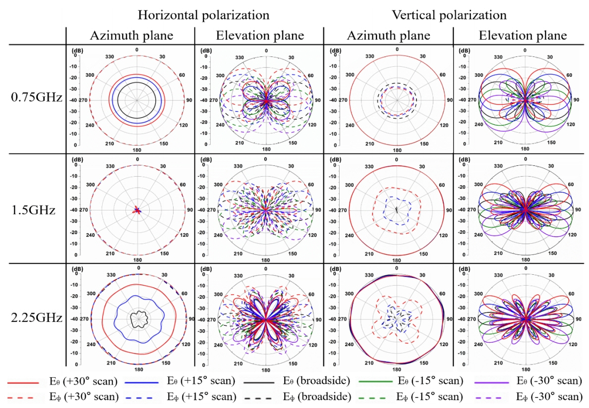
The normalized radiation patterns of the eight-layer C-TCDA for the horizontal and vertical polarizations are presented in Fig. 9. As expected, the E
Žå components are predominantly observed when the horizontal polarization dipoles are excited, and the E
╬Ė components are predominantly observed when the vertical polarization dipoles are excited. The C-TCDA has good omnidirectional patterns in the azimuthal plane for both polarizations. In the elevation plane pattern, the C-TCDA can scan in the desired direction up to ┬▒30┬░ for both polarizations. Most of the patterns show a low cross-polarization under ŌłÆ10 dB compared with the copolarization and a sidelobe under ŌłÆ10 dB.
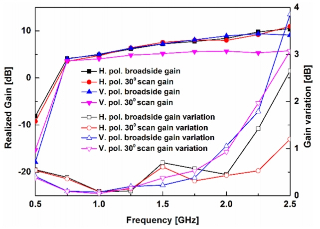
The realized gain and gain variation of the eight-layer C-TCDA versus frequency graphs radiating at broadside (0┬░) and scanning to 30┬░ are shown in Fig. 10. The gain and gain variation values for the scan angles between 0┬░ and 30┬░ are between the values when the scan angle is 0┬░ and 30┬░. The realized gain has a range of 4ŌĆō9.3 dB and 3.6ŌĆō5.7 dB for 0┬░ and up to ┬▒30┬░, respectively. Moreover, the gain variation in the azimuthal plane is lower than 1.8 dB and 2 dB for 0┬░ and up to ┬▒30╦Ü, respectively.
For practical implementation, the C-TCDA elements must be finite in the z-direction. Most studies on planar TCDAs show that TCDAs using 8 ├Ś 8 or more elements perform similarly to the infinite case [10ŌĆō12]. Therefore, there should be little difference in performance between a practical N ├Ś M (Ōēź8) C-TCDA and the N ├Ś infinite C-TCDA simulated in this design.
IV. Conclusion
We analyzed a C-TCDA and proposed the design of a wideband dual-polarized array antenna for an omnidirectional pattern. Similar to that in the planar TCDA, the radiation wave can exist as a TEM mode in the C-TCDA. Moreover, the embedding impedance characteristics of the C-TCDA for both polarizations resemble those of the planar TCDA. The proposed C-TCDA antenna has a wide bandwidth of 3.08:1 (0.73ŌĆō2.25 GHz) with an omnidirectional radiation pattern in the horizontal plane, a low cross-polarization level of 10 dB, and a wide scanning angle of up to ┬▒30┬░. We consider that our C-TCDA theory and design can be applied to modern communication systems, such as indoor distributed antenna systems, base station antennas, and conformal array antenna systems for electric warfare.