Design Method for Negative Group Delay Circuits Based on Relations among Signal Attenuation, Group Delay, and Bandwidth
Article information
Abstract
Typical negative group delay circuits (NGDC) are analyzed in terms of signal attenuation, group delay, and bandwidth using S-parameters. By inverting these formulations, we derive and present the design equations (for NGD circuit elements) for a desired specification of the two among the three parameters. The proposed design method is validated through simulation examples for narrow- and wide-band pulse inputs in the time and frequency domains. Moreover, an NGDC composed of lumped elements is fabricated at 1 GHz for measurement. As a function of frequency, the circuit-/EM-simulated and measured group delays are in good agreement. The provided simple NGDC design equations may be useful for many applications that require compensations of some signal delays.
I. Introduction
Negative group delay (NGD) was initially presented by Brillouin [1] in the 1960s, and it has been studied actively since the research on superluminal effects was published in [2]. The NGD characteristics have been demonstrated in various systems. In the microwave area, NGD circuits are used to compensate for group delays usually caused by the use of filters or amplifiers [3, 4]. Many studies have been conducted to utilize the NGD phenomenon by employing various structures, such as a defected microstrip structure and a defected ground structure [5]. In [6], the familiarity between a non-Foster reactive property and NGD networks with loss compensation was discussed theoretically and experimentally. A loss-compensated NGD network composed of cascading two unit cells and amplifiers was also presented for larger NGD effects. Some design equations were proposed through an S-parameter analysis [6–9], a lossy coupling matrix synthesis [10], and a filter analysis [11]. The design equations for negative group delay circuit (NGDC) using lumped RLC resonators are also available based on the specification of the signal attenuation and NGD [12, 13]. In this study, we derive the mathematical relations among signal attenuation, NGD, and bandwidth for a convenient and systematic design of the NGDC composed of RLC resonators. The effects of the NGDC are evaluated in the time and frequency domains using narrow- and wide-band pulse inputs. To verify the proposed design equations, we fabricate an NGDC composed of lumped elements at 1 GHz. The group delays of the fabricated NGDC are measured and compared with those obtained from the presented design equations.
II. Analysis and Synthesis of a Group Delay Circuit
1. Analysis
Fig. 1(a) shows an equivalent circuit consisting of a parallel resonant circuit connected in a series with a transmission line. Z0 is the characteristic impedance of the host transmission line. Fig. 1(b) shows an equivalent circuit consisting of a series resonant circuit connected in parallel with a transmission line. Y0 is the characteristic admittance. Most passive NGD structures can be modeled on the basis of these equivalent circuits in Fig. 1(a) and (b).
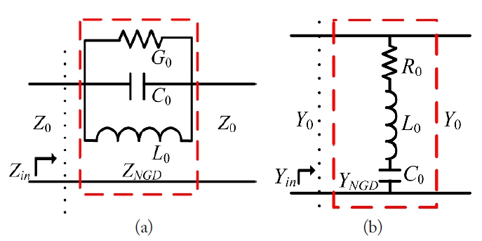
(a) Equivalent circuit for the NGD structure made of a parallel GCL resonator connected in a series with a transmission line. (b) Equivalent circuit for the NGD structure made of a series RLC resonator connected in parallel with the transmission line.
In Fig. 1(a), the admittance of YNGD of the parallel resonant circuit can be expressed as
where G0 is the conductance, ω is the angular frequency, ω0 is the resonant angular frequency given by
The impedance ZNGD can be approximated as
Then, the input impedance Zin is the sum of ZNGD and Z0. The reflection coefficient S11 is obtained as
When ω=ω0, S11 (3) is simplified to
The transmission coefficient (S21) of the NGDC unit cell can be obtained by the ratio of the transmitted voltage (
The real and imaginary parts of S21 are represented by
and
respectively.
S21 (5) at ω0 is simplified to
which is purely real and positive. That is, the transmission at ω0 across the NGDC in Fig. 1(a) occurs without a phase delay. The phase for the NGDC is obtained as
Then, the group delay (τ) [8] can be shown to be given by
which is negative, and its magnitude is observed to become maximum at the resonant angular frequency ω0 and zero when ω is far away from ω0. The group delay is another word for a signal envelope delay [14]. The frequency dependence in (10) prevents a pulse input from being entirely copied in advance of the input at the output terminal. The maximum NGD is expressed as
As G0 becomes smaller, the signal transmission becomes smaller, as implied by (8), but the effect of the NGD becomes larger, as shown by (11). The magnitude of the NGD is shown to be proportional to C0 as is the susceptance slope ω0C0.
Fig. 2 shows the magnitudes and phases of S21 when τ(ω0) (11) is assumed to be −0.5, −1, and −5 ns and S21(ω0)= 0.5 at 1 GHz. In the case of τ(ω0) = −1 ns, Z0 = 50 Ω, G0 = 1/100 (1/Ω), C0 = 10 pF, and L0 = 2.53 nH. As the magnitude of τ(ω0) becomes larger, the bandwidth of the NGD becomes smaller. This will result in more signal distortion if an input signal bandwidth is wider than the NGDC bandwidth. The positive phase slopes near 1 GHz shown in Fig. 2(b) lead to NGD s, as explained in (10).

(a) Magnitudes of S21. (b) Phases of S21 for different group delays when S21(ω0) is fixed at 0.5 at 1 GHz.
So far, we have analyzed the NGD equivalent circuit given in Fig. 1(a) in terms of the signal transmission S21 and NGD τ.
2. Synthesis
On the contrary, if specific values of S21(ω0) and τ(ω0) are desired for a particular NGD circuit design, (8) and (11) can be simultaneously solved for the design equations given by
and L0 is obtained with
Fig. 3 shows the capacitance values of the NGD circuit for different S21(ω0) and τ(ω0) at 1 GHz using (13). Whereas G0 (12) depends only on S21(ω0), C0 and L0 depend on both S21(ω0) and τ(ω0). Expressions (12)–(14) are actually the design equations to realize the specifically required values of S21(ω0) and τ(ω0). With (12) and (13), the quality factor of the NGD circuit may be expressed as

Capacitance values for different S21(ω0) and τ(ω0).
Moreover, the 3 dB fractional bandwidth (BW) is roughly given by
The bandwidth (16) becomes large as S21(ω0) (8) or τ(ω0) (11) becomes small. Note that if the two among the three design parameters S21(ω0) (8), τ(ω0) (11), and bandwidth (16) are specified, the rest is determined automatically. This relation is summarized in Table 1.
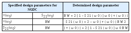
Relation among design parameters S21(ω0), τ(ω0), and BW
Fig. 4(a) shows the group delay τ(ω) (10) as a function of frequency for different S21(ω0)’s of −6, −10, and −20 dB when τ(ω0) is −1 ns at 1 GHz. As S21(ω0) becomes smaller, the bandwidth of τ(ω) becomes larger; this is the important tradeoff feature of the presented NGDC. Fig. 4(b) shows S21(ω) as a function of frequency for the different S21(ω0)’s of −10, −20, −30, and −40 dB when τ(ω0) is fixed at −1 ns at 1 GHz. The symbols represent the calculated results using (5), and the lines represent the circuit-simulated results based on Fig. 1(a).
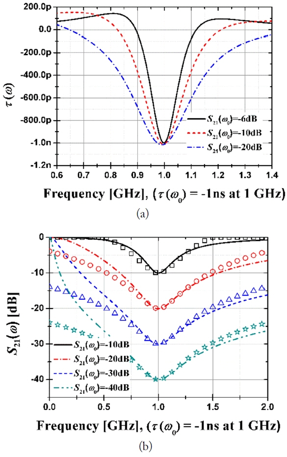
In Table 2, we show the Q factors and compare the bandwidths based on (16) and circuit simulations. The results in Fig. 4(b) and Table 2 prove the theory to be accurate enough when ω is near ω0.

Q-factors and bandwidth for the different S21(ω0)’s of −10, −20, −30, and −40 dB when τ(ω0)= −1 ns at 1 GHz
In Fig. 5, we show the 3 dB fractional bandwidth (16) of the NGDC as a function of S21(ω0) and τ(ω0). The bandwidth increases as S21(ω0) decreases and |τ(ω0)| gets smaller.

The 3-dB bandwidth of NGDC as a function of S21(ω0) and τ(ω0) at 1 GHz.
Table 3 shows the circuit element values of the NGDC obtained using the design Eqs. (12)–(14) assuming that
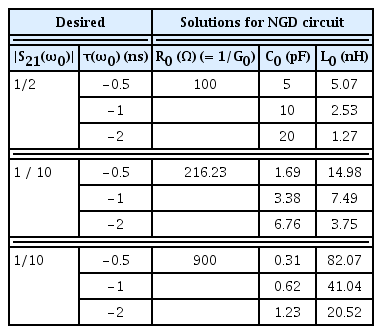
Calculated circuit values for specific examples
Fig. 6 shows the diagram of the NGDC combined with an amplifier. The attenuated signal through the NGDC is shown to be properly amplified using the amplifier. The output signal may be somewhat distorted because the bandwidth of the NGDC is usually smaller than the bandwidth of the input signal.
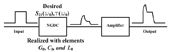
Diagram of the NGDC combined with an amplifier (brief sketches of the input and output are shown).
Fig. 7 shows the envelopes and spectra of the input and output signals. The rising/falling time and the width of the input pulse are 3 ns and 1 ns, respectively. The 1 GHz carrier signal is shown only in Fig. 7(a) and is hidden in Fig. 7(b). The output with the NGDC is shown to have some NGD features with an attenuation of about 1/10. The effect of NGD is more pronounced after amplification 10 times. The spectrum of the output has more high-frequency components than that of the input, consistent with the time signals in Fig. 7(b).
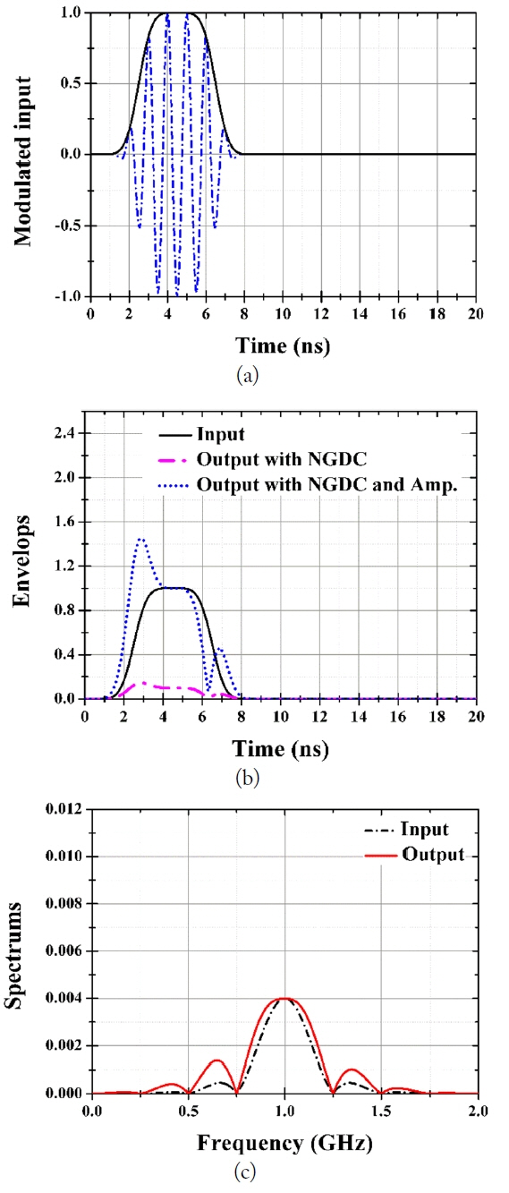
(a) Modulated input signal and carrier as a function of time. The rising/falling time and the width of the input pulse are 3 ns and 1 ns, respectively. The carrier frequency is 1 GHz. (b) Envelopes of the input and output as a function of time with the desired τ(ω0) = −1 ns and S21(ω0) = −20 dB. (c) Spectra of the input and output as a function of frequency.
In Fig. 8(a), we show the envelopes of the input and output signals with τ(ω0) = −1 ns and −2 ns, respectively. The rising/falling time and the width of the input pulse are 3 ns and 3 ns, respectively. The carrier frequency is again 1 GHz but not shown. As the magnitude of τ(ω0) increases, the output appears more ahead of the input pulse, but its distortion compared with the input pulse becomes larger. In Fig. 8(b), we show the same when τ(ω0) = −1, −2, and −5 ns. For this case, the rising/falling time and the width of the input pulse are 6 ns and 6 ns, respectively. The input pulse in Fig. 8(b) is slowly varying, and its spectrum should be narrower than that in Fig. 8(a). This leads to less distortion as demonstrated particularly in the case of τ(ω0) = −2 ns.
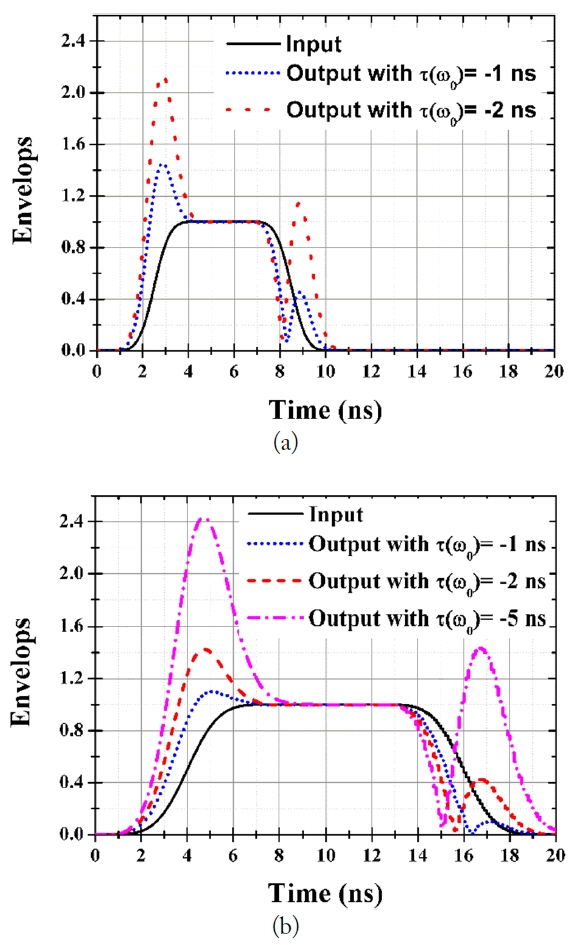
(a) Circuit-simulated envelopes of the input and output signals as a function of time with the desired S21(ω0) = −20 dB for different τ(ω0) = −1 ns and −2 ns. The rising/falling time and the width of the input pulse are 3 ns and 3 ns, respectively. The hidden carrier frequency is 1 GHz. (b) Envelopes of the input and output as a function of time with the desired S21(ω0) = −20 dB for different τ(ω0) = −1, −2, and −5 ns. The rising/falling time and the width of the input pulse are 6 ns and 6 ns, respectively. The hidden carrier frequency is 1 GHz.
Fig. 9(a) shows the structure of the proposed NGDC composed of lumped RLC elements based on the required S21(ω0) = −20 dB and τ(ω0) = −1 ns at 1 GHz. Fig. 1(b) is the photograph of the measurement setup. The permittivity of the microstrip transmission line with a thickness of 1.6 mm and the lumped element values are ɛr = 2.2, R0 = 900 Ω, C0 = 0.62 pF, and L0 = 41 nH using (12)–(14). The S-parameters of the structure are measured using a network analyzer. The influence of the transmission line is de-embedded on the reference plane at the center of the structure.
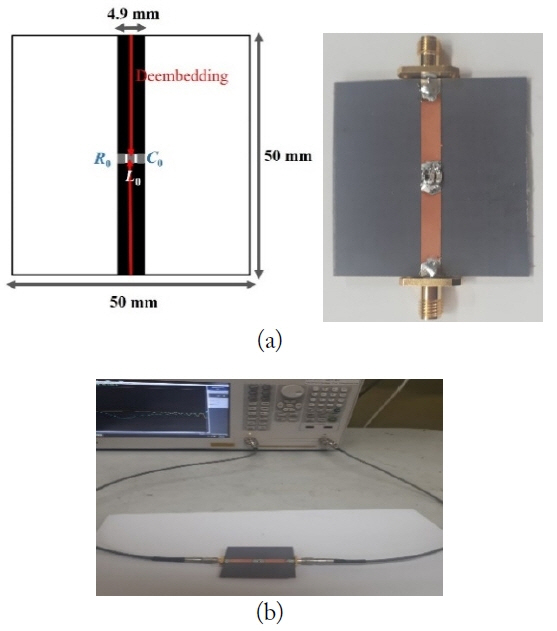
(a) Fabricated NGDC composed of lumped RLC elements based on the required S21(ω0) = −20 dB and τ(ω0) = −1 ns at 1 GHz (ɛr = 2.2, thickness = 1.6 mm, R0 = 900 Ω, C0 = 0.5 pF, and L0 = 33 nH). (b) Photograph of the measurement setup.
Table 4 presents the circuit element values calculated using Eqs. (12)–(14), tuned by electromagnetic (EM) simulations, and used for fabrication. The values tuned by the EM simulations are different from the theoretical ones. The actually used element values are the ones closest to the available ones.
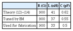
Lumped element values for the case in which S21(ω0) = −20 dB and τ(ω0) = −1 ns at 1 GHz
Fig. 10 shows the circuit-/EM-simulated and measured S-parameters and group delays as a function of frequency in the case shown in Fig. 9. They all show to be in good agreement. The output time signals to the input pulses are similar to the dotted ones with τ(ω0) = −1 ns in Fig. 8(a).
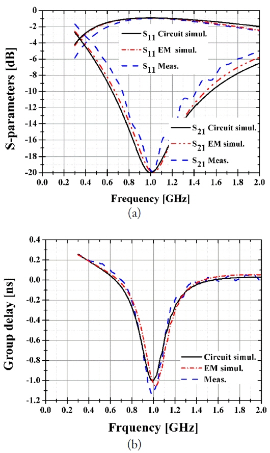
Circuit-/EM-simulated and measured results of the NGD circuit when S21(ω0) = −20 dB and τ(ω0) = −1 ns at 1 GHz. (a) S-parameters S(ω). (b) Group delay τ(ω).
In the case of using N unit cells in Fig. 1(a), (8) can be shown to be generalized to
and (11) to
As the number N of the identical unit cells increases, the signal transmission (17) decreases but the NGD (18) does not change much.
In the case of the NGDC in Fig. 1(b), the analysis and design equations are obtained by simply converting Z0, G0, C0, L0, and Zin in this study to Y0, R0, L0, C0, and Yin using the duality principle. The presented design method is applicable to other previous passive NGD circuits, not just the one demonstrated in this study.
III. Conclusion
Then characteristics of NGD circuits are systematically characterized using S21(ω0), τ(ω0), and bandwidth. Some design examples are provided and analyzed in the time and frequency domains. The relations among S21(ω0), τ(ω0), and the group delay bandwidth are explained using closed-form expressions. The circuit-/EM-simulated and the measured S-parameters and group delays are all shown to be in good agreement. The presented NGDC design methods may be useful for many applications, such as filters, feed-forward amplifiers, array antennas, and non-Foster reactive elements, among others.
Acknowledgements
This work was supported by the Institute for Information & Communications Technology Promotion (IITP) grant funded by the Korea government (MSIT) (No. IITP-2019-2016-0-00291, Information Technology Research Center).
References
Biography
Sehun Na received his B.S. degree in electronics engineering from Kyung Hee University, Yongin, Korea, in 2016. He is currently pursuing his master’s degree in electronics engineering from Kyung Hee University. His research interests include wireless power transfer systems, passive devices, and small antennas.

Youn-Kwon Jung (M’09) received his B.S. degree in radio communication engineering from Kyung Hee University, Yongin, Korea, in 2008 and his M.S. and Ph.D. degrees in electronics and radio engineering from the same university in 2011 and 2016, respectively. In 2016, he joined Hanwha Systems, where he is currently a senior researcher at an Active Electronically Steering Array (AESA) radar research center. His research interests include AESA antennas, system antenna, microwave passive devices, small antennas, RFID reader antennas, wireless power transmission, and metamaterials.

Bomson Lee (M’96) received his B.S. degree in electrical engineering from Seoul National University, Seoul, Korea, in 1982. From 1982 to 1988, he worked at Hyundai Engineering Company Ltd., Seoul, Korea. He received his M.S. and Ph.D. degrees in electrical engineering from the University of Nebraska, Lincoln, NE, USA in 1991 and 1995, respectively. In 1995, he joined the faculty of Kyung Hee University, where he is currently a professor at the Department of Electronics Engineering. From 2007 to 2008, he was the chair of the technical group for microwave and radio wave propagation in the Korea Institute of Electromagnetic Engineering & Science (KIEES). In 2010, he was Editor-in-Chief of the Journal of the Korean Institute of Electromagnetic Engineering and Science. He was vice-chairman in 2015–2016 and executive vice-chairman of KIEES in 2017. Since 2018, he has been the president of KIEES. His research interests include microwave antennas, RF identification tags, microwave passive devices, wireless power transfer, and metamaterials.