A Decade-Bandwidth Distributed Power Amplifier MMIC Using 0.25 μm GaN HEMT Technology
Article information
Abstract
This study presents a 2–20 GHz monolithic distributed power amplifier (DPA) using a 0.25 μm AlGaN/GaN on SiC high electron mobility transistor (HEMT) technology. The gate width of the HEMT was selected after considering the input capacitance of the unit cell that guarantees decade bandwidth. To achieve high output power using small transistors, a 12-stage DPA was designed with a nonuniform drain line impedance to provide optimal output power matching. The maximum operating frequency of the proposed DPA is above 20 GHz, which is higher than those of other DPAs manufactured with the same gate-length process. The measured output power and power-added efficiency of the DPA monolithic microwave integrated circuit (MMIC) are 35.3–38.6 dBm and 11.4%–31%, respectively, for 2–20 GHz.
I. Introduction
Recently developed microwave systems require increasingly wider operating bandwidth. Especially electronic warfare systems are required to operate in multi-octave bandwidth. An ultra-wideband power amplifier is one of the most challenging components to be implement in electronic warfare systems. Currently, such ultra-wideband power amplifier can be implemented with AlGaN/GaN high electron mobility transistor (HEMT) monolithic microwave integrated circuit (MMIC) technology, which has rapidly developed over the past several years [1].
Compared to other amplifier structures that use lossy matching or balanced topologies, a distributed amplifier (DA) is advantageous for wideband operations because in the DA configuration gate-source capacitance and drain-source capacitance of each transistor are absorbed into the artificial transmission line structure. The bandwidth of the DA is determined by the dominant low-pass cutoff frequency of input or output artificial transmission lines [2]. Therefore, the smaller capacitance of the transistor results in wider bandwidth in the DA configuration.
This paper presents the design and fabrication of a distributed power amplifier (DPA) MMIC with decade-bandwidth using 0.25 μm GaN HEMT technology. The maximum operating frequency of the proposed DPA is above 20 GHz, which is higher than those of other DPAs manufactured using the same gate-length process.
II. Unit Cell Design for Bandwidth Enhancement
The DPA MMIC fabrication process is GH25-10 of United Monolithic Semiconductors, which provides 0.25 μm AlGaN/GaN HEMTs on SiC substrates. The gate capacitance in the input transmission line has a value substantially larger than the drain capacitance in the output transmission line and determines the dominant cutoff frequency of the DPA [2]. For the DPA to have a cutoff frequency of over 20 GHz, the gate capacitance of a constituent unit cell should be less than 0.3 pF. A schematic diagram and an input equivalent circuit of the unit cell are illustrated in Fig. 1. The gate-source capacitance, Cgs, and distributed channel resistance, Ri, are input intrinsic elements of GaN HEMT. These intrinsic elements could be extracted through small-signal admittance parameters. The RS-CS parallel network is intentionally inserted to extend the cutoff frequency and stabilizes the amplifier.
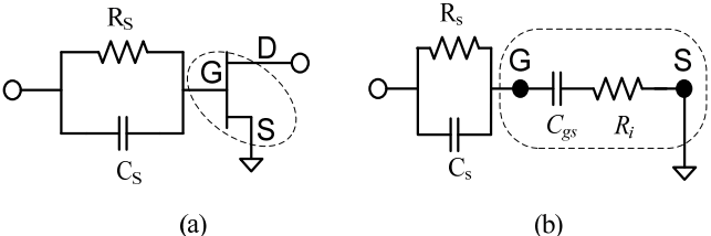
(a) Schematic diagram of capacitive coupled GaN HEMT and (b) input equivalent circuit at the gate.
The gate capacitance of the unit cell can be reduced through insertion of a series-connected coupling capacitor (Cs). However, in a large peripheral HEMT, the Cgs tends to increase rapidly with the frequency, which limits the peripheral size of the HEMT that can be used to achieve a multi-octave band DPA. Fig. 2 shows the equivalent capacitance of a unit cell composed of 4 × 100 μm HEMT and Cs of 0.3 pF and a unit cell composed of 4 ×50 μm HEMT and Cs of 0.3 pF. Applying the former to the DPA design is advantageous in obtaining larger output power, but the operating frequency is restricted to less than 16 GHz. Therefore, the latter should be selected in order to obtain a sufficiently high cutoff frequency above 20 GHz.
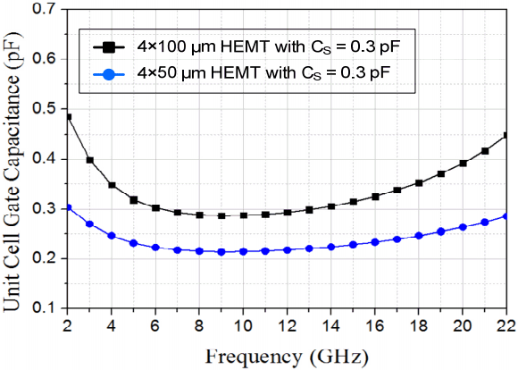
Equivalent gate capacitance of unit cell with frequency.
III. Distributed Power Amplifier Design
A conventional DPA, called as a non-uniform DPA (NDPA), is designed using non-uniform drain lines, non-uniform transistor size or both to improve an output power and a power-added efficiency (PAE) [3, 4]. The schematic circuit diagram of the DPA is shown in Fig. 3. In an NDPA architecture, the device size of the first cell (Q1) is usually larger than those of the rest unit cells for optimal power matching. However, in this study, we used 4 × 50 μm HEMTs in all unit cells to extend the bandwidth.
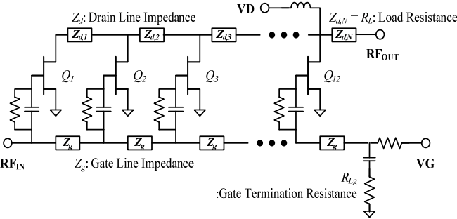
Schematic diagram of the proposed bandwidth-enhanced DPA.
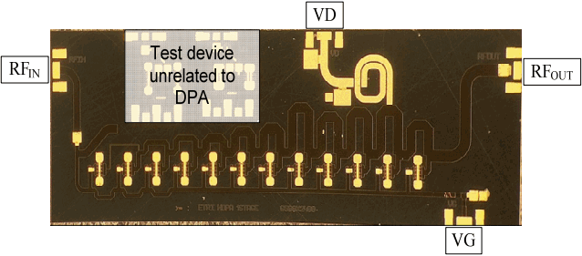
The use of small peripheral HEMTs slightly reduces the output power but can increase the number of stages in the DPA because large characteristic impedances are required for optimal power matching in the drain lines. We used 12 stages in the DPA to increase the output power within the feasible characteristic impedance range of the drain line. Layout effects including transmission lines, discontinuities and inductors were electro-magnetically simulated to include coupling and radiation effects. A photograph of the fabricated decade-bandwidth DPA MMIC is shown in Fig. 4. The chip dimensions are 6.45 mm × 2.35 mm.
Photograph of the decade bandwidth DPA MMIC.
IV. Measured Results
The fabricated DPA MMIC was mounted on a test jig for the measurement. The test jig consists of a carrier with a power circuit board, two 50-Ω lines, an aluminum housing and two K-connectors. The DPA MMIC is biased at a drain-source voltage of 28 V and a drain current of 600 mA. The small- and large-signal measurements were performed in continuous mode.
Fig. 5 shows the measured and simulated S-parameters of the DPA MMIC. Measured small signal gain is 8.4–11.2 dB, and the input/output return losses are typically 10 dB or more from 2 to 20 GHz. The measured output power and PAE of the DPA MMIC are shown in Fig. 6. In 2–20 GHz, the output power is 35.3–38.6 dBm and the PAE is 11.4%–31%.
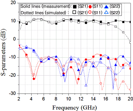
Measured and simulated S-parameters of the DPA MMIC.
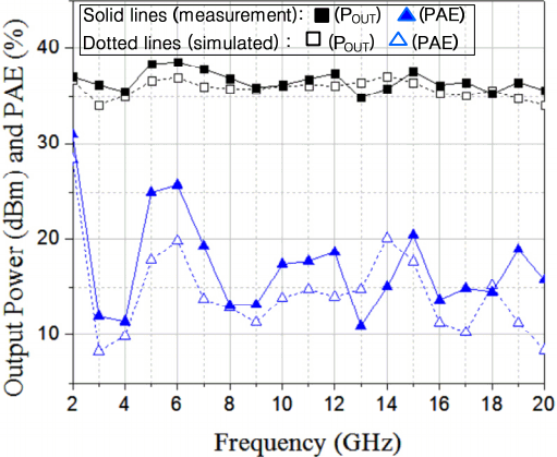
Measured and simulated output power and PAE of the DPA MMIC.
The performance of state-of-the-art DPA MMICs fabricated using the 0.25 μm GaN HEMT process is summarized in Table 1. Regarding the operating frequency, this work is competitive with state-of-the-art results.
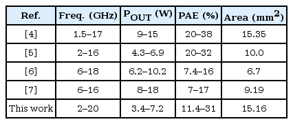
Performance comparison of GaN DPA MMICs fabricated using a 0.25 μm GaN process
V. Conclusion
A 2–20 GHz DPA MMIC was demonstrated using a 0.25 μm GaN HEMT process, and the results were presented. The proposed DPA successfully achieved flat gain and output power up to 20 GHz through the design of a unit cell that supported decade bandwidth.
Acknowledgements
This work was supported by National Research Foundation of Korea (NRF) grant funded by the Korea government (MSIP) (No. NRF-2015M1A3A3A03027459).